

Fairchild Semiconductor 74ACTQ16543SSCX, 74ACTQ16543SSC, 74ACTQ16543MTDX, 74ACTQ16543MTD, 74ACTQ16543CW Datasheet
December 1991
Revised December 1998
74ACTQ16543 16-Bit Register ed Transceiver with 3-STATE Outputs
© 1999 Fairchild Semiconductor Corporation DS010967.prf www.fairchildsemi.com
74ACTQ16543
16-Bit Registered Transceiver with 3-STATE Outputs
General Description
The ACTQ16543 contains sixtee n non-inverting transc eivers containing two sets of D-type registers for temporary
storage of data flowing in ei ther direction. Each byte has
separate control inputs whi ch can be short ed together for
full 16-bit operation. Separate Latch Enable and Output
Enable inputs are provided for each register to permit independent input and o utput contr ol in either directio n of data
flow.
The ACTQ16543 utilizes Fairchild Quiet Series technology to guarantee quiet output switching and improved
dynamic threshold performa nce. FACT Quiet Series features GTO output control and under shoot corrector for
superior performance.
Features
■ Utilizes Fairchild FACT Quiet Series technology
■ Guaranteed simultaneous switching noise level and
dynamic threshold performance
■ Guaranteed pin-to-pin output skew
■ Independent registers for A and B buses
■ Separate controls for data flow in each direction
■ Back-to-back registers for storage
Multiplexed real-time and stored data transfers
■ Separate control logic for each byte
■ 16-bit version of the ACTQ543
■ Outputs source/sink 24 mA
■ Additional specs for Multiple Output Switching
■ Output loading specs for both 50 pF and 250pF loads
Ordering Code:
Device also available in Tape and Reel. Specify by appendin g s uf f ix let t er “X” to the ordering co de.
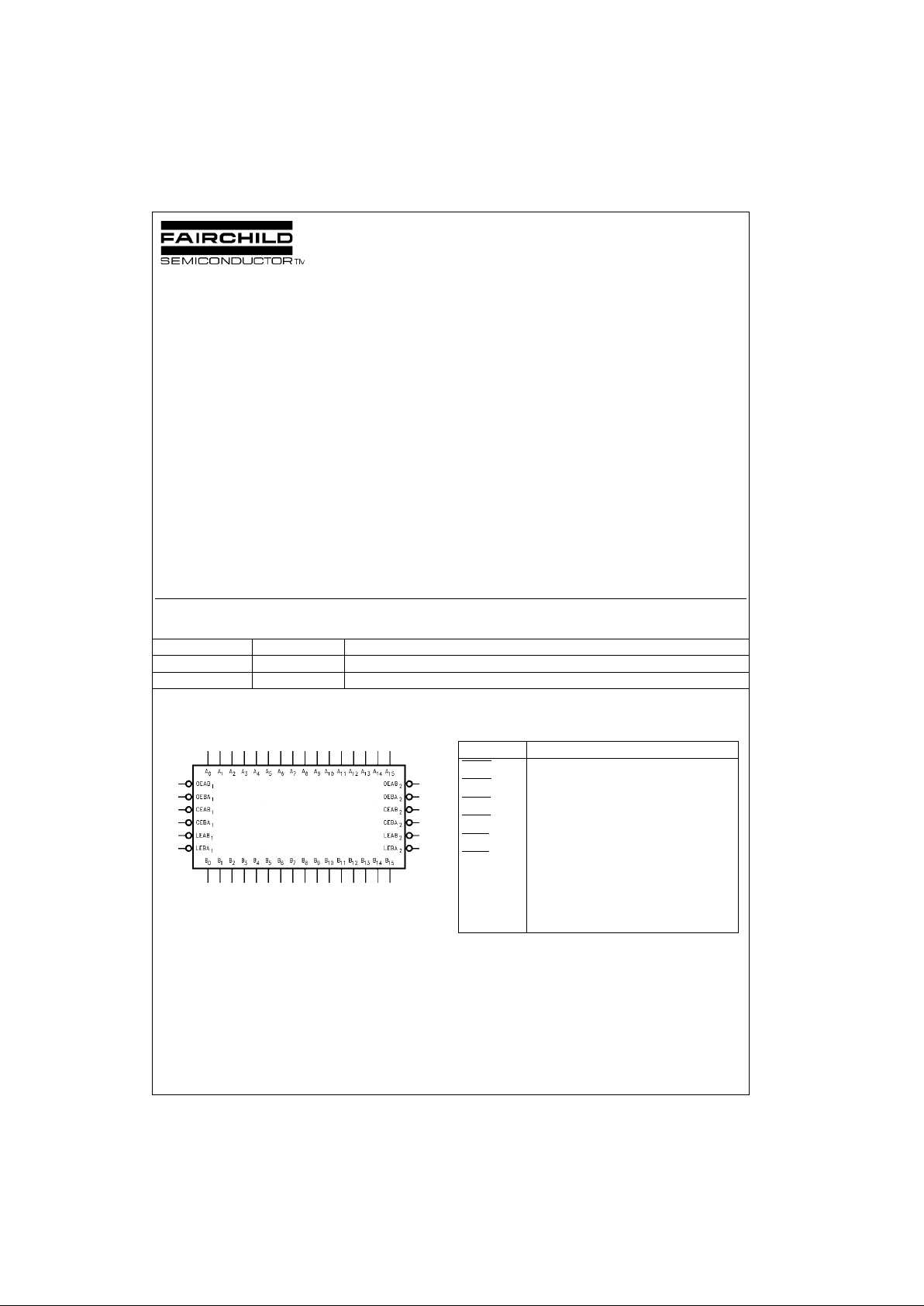
Logic Symbol Pin Descriptions
FACT, Quiet Series, FACT Quiet Series and GTO are trademarks of Fairchild Semiconductor Co rporation.
Order Number Package Number Package Description
74ACTQ16543SSC MS56A 56-Lead Shrink Small Outline Package (SSOP), JEDEC MO-118, 0.300” Wide
74ACTQ16543MTD MTD56 56-Lead Thin Shrink Small Outline Package (TSSOP), JEDEC MO-153, 6.1mm Wide
Pin Names Descriptions
OEAB
n
A-to-B Output Enable Input (Active LOW)
OEBA
n
B-to-A Output Enable Input (Active LOW)
CEAB
n
A-to-B Enable Input (Active LOW)
CEBA
n
B-to-A Enable Input (Active LOW)
LEAB
n
A-to-B Latch Enable Input (Active LOW)
LEBA
n
B-to-A Latch Enable Input (Active LOW)
A
0–A15
A-to-B Data Inputs or
B-to-A 3-STATE Outputs
B
0–B15
B-to-A Data Inputs or
A-to-B 3-STATE Outputs
www.fairchildsemi.com 2
74ACTQ16543
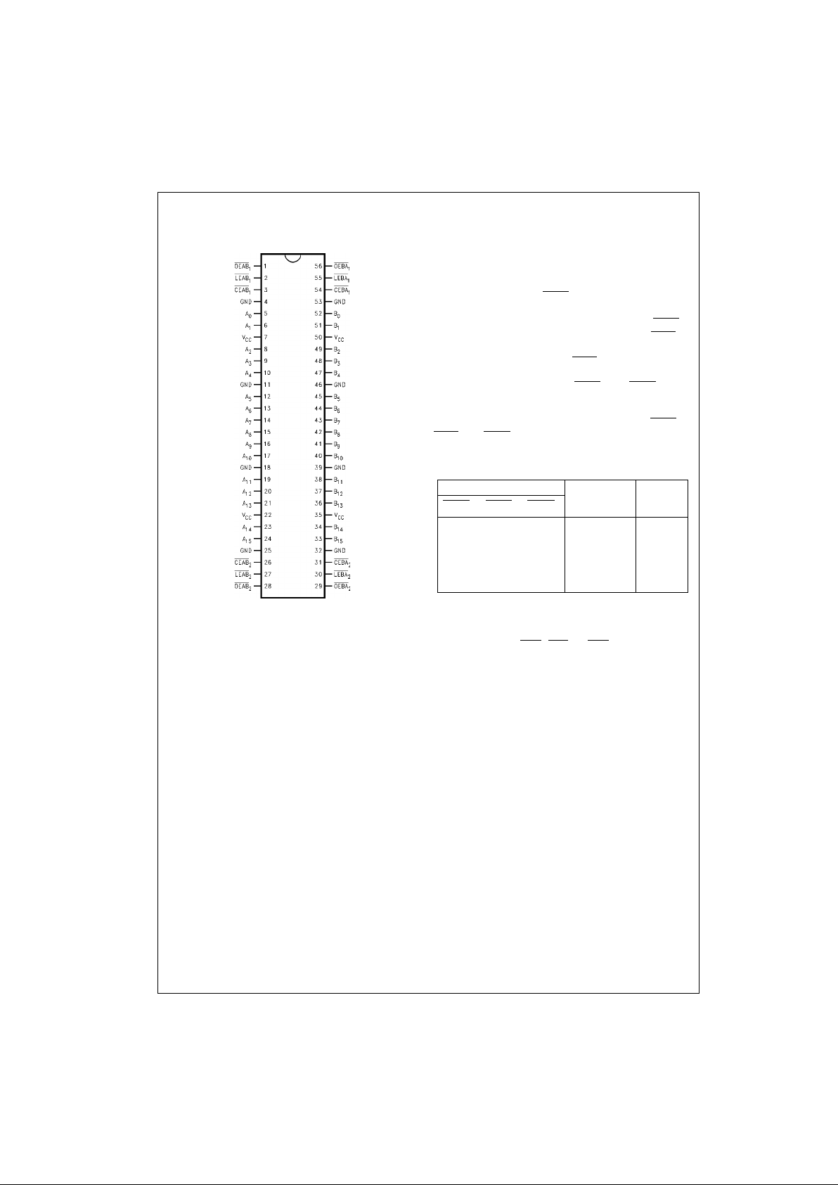
Connection Diagram
Pin Assignment for SSOP and TSSOP
Functional Description
The ACTQ16543 contains sixte en non-inverting trans ceivers with 3-STATE outputs. The device is byte controlled
with each byte functioning ide ntically, but inde pendent of
the other. The control pins may be shorted together to
obtain full 16-bit operation. The following description
applies to each byte. For data flow from A to B, for example, the A-to-B Enable (CEAB
n
) input must be LOW in
order to enter data from A
0–A15
or take data from B0–B15,
as indicated in the Data I/O Control Table. With CEAB
n
LOW, a LOW signal on the A-to-B Latch Enable (LEABn)
input makes the A-to-B latches transparent; a subsequent
LOW-to-HIGH transition of the LEAB
n
signal puts the A
latches in the storage mode and their outputs no longer
change with the A inputs. With CEAB
n
and OEABn both
LOW, the 3-STATE B output buffers are active and reflect
the data present at t he output of the A la tches. Control of
data flow from B to A is similar, but using the CEBA
n
,
LEBA
n
and OEBAn inputs.
Data I/O Control Table
H = HIGH Voltage Level
L = LOW Voltage Level
X = Immaterial
A-to-B data flow shown; B-t o-A flow control
is the same, except using CE BA
n
, LEBAn and OEBA
n
Inputs Latch Status
(Byte n)
Output
Buffers
(Byte n)
CEAB
n
LEABnOEAB
n
H X X Latched High Z
X H X Latched —
L L X Transparent —
X X H — High Z
L X L — Driving
3 www.fairchildsemi.com
74ACTQ16543
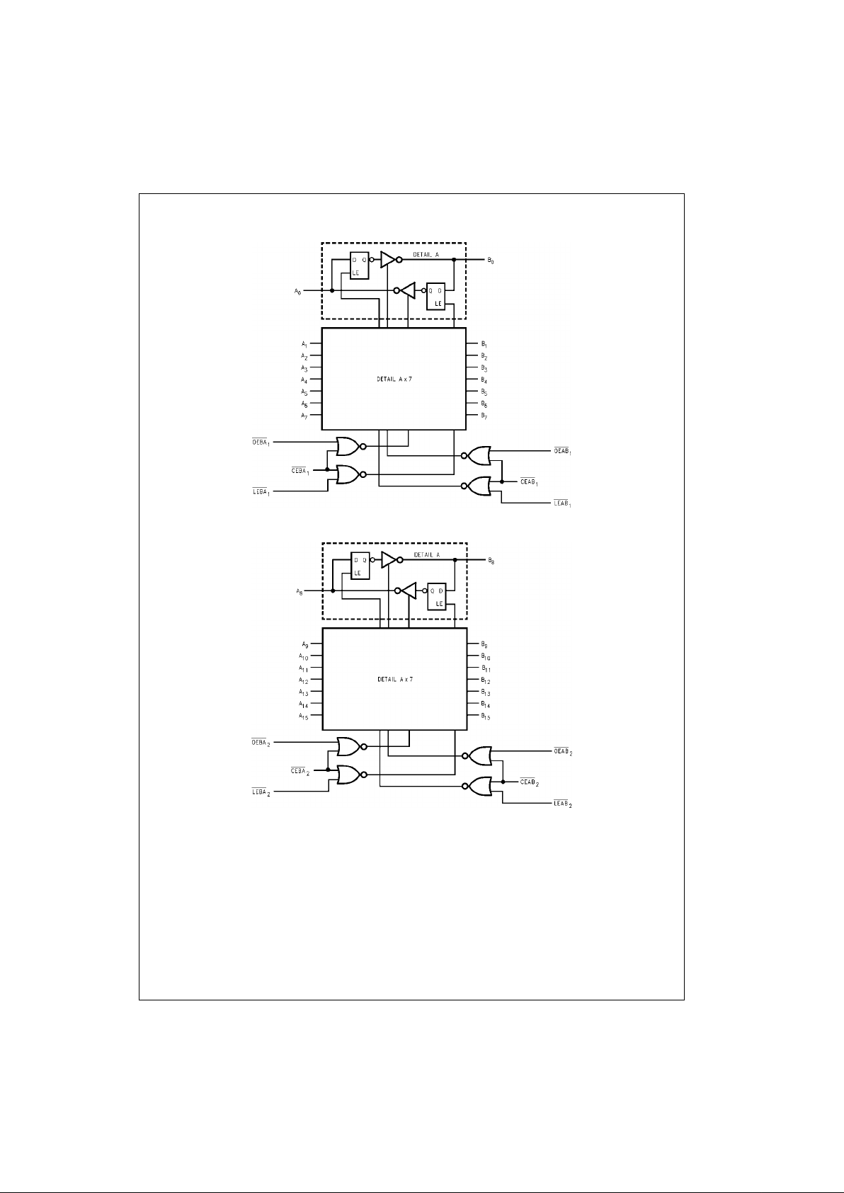
Logic Diagrams
Byte 1 (0:7)
Please note that this d iagram is provided only for the understanding of logic operations and should no t b e us ed to estimate propagation delays.
Byte 2 (8:15)
Please note that this d iagram is provided only for the understanding of logic operations and should no t b e us ed to estimate propagation delays.
 Loading...