

Fairchild Semiconductor 74ACTQ16245CW, 74ACTQ16245SSCX, 74ACTQ16245SSC, 74ACTQ16245MTD Datasheet
© 1999 Fairchild Semiconductor Corporation DS010926 www.fairchildsemi.com
May 1991
Revised November 1999
74ACTQ16245 16-Bit Transceiver with 3-STATE Outputs
74ACTQ16245
16-Bit Transceiver with 3-STATE Outputs
General Description
The ACTQ16245 contains sixteen non-inverting bidirectional buffers with 3-STATE outputs and is intended for bus
oriented applications. The device is byte control led. Each
has separate control input s which can be shorted tog ether
for full 16-bit operation. The T/R
inputs determine the direc-
tion of data flow throu gh t he d evice . T he O E
inputs disable
both the A and B ports by placing them in a high i mpedance state.
The ACTQ16245 utilizes Fairchild Quiet Series technology to guarantee quiet output switching and improved
dynamic threshold perf ormance. FACT Quiet Series fe atures GTO output control for superior performance.
Features
■ Utilizes Fairchild FACT Quiet Series technology
■ Guaranteed simultaneou s switching nois e level and
dynamic threshold performan ce
■ Guaranteed pin-to-pin output skew
■ Bidirectional non-inverting buffers
■ Separate control logic for each byte
■ 16-bit version of the ACTQ245
■ Outputs source/sink 24 mA
■ Additional specs for multiple output switching
■ Output loading specs for both 50 pF and 250 pF loads
Ordering Code:
Device also available in Tape and Reel. Specify by appending s uffix let te r “X” to the ordering code.
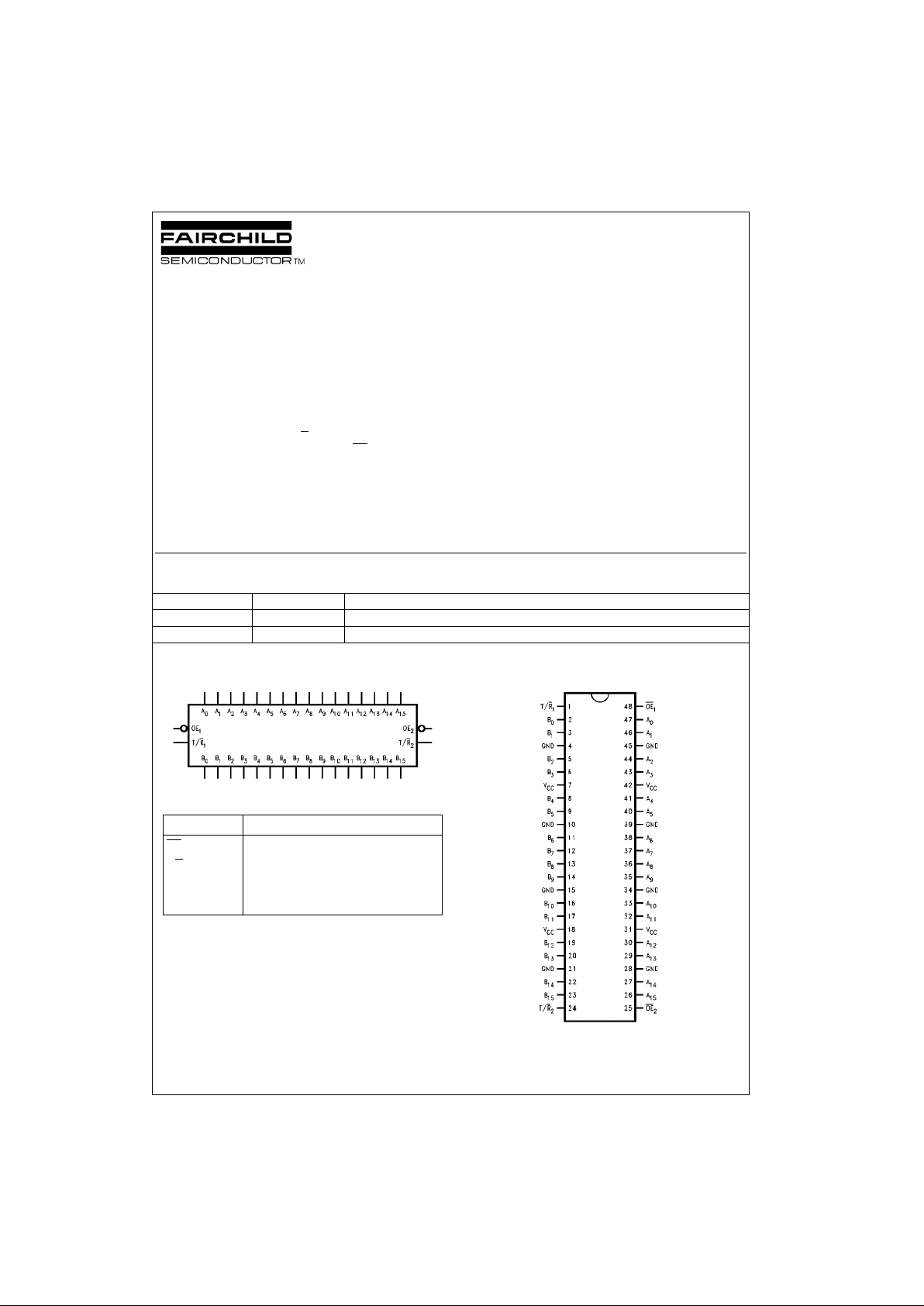
Logic Symbol
Pin Description
Connection Diagram
FACT, FACT Quiet Series and GTO are trademarks of Fairchild Semiconductor Corporation.
Order Number Package Number Package Description
74ACTQ16245SSC MS48A 48-Lead Small Shrink Outline Package (SSOP), JEDEC MO-118, 0.300” Wide
74ACTQ16245MTD MTD48 48-Lead Thin Shrink Small Outline Package (TSSOP), JEDEC MO-153, 6.1mm Wide
Pin Names Description
OE
n
Output Enable Input (Active LOW)
T/R
Transmit/Receive Input
A
0–A15
Side A Inputs/Outputs
B
0–B15
Side B Outputs/Inputs

www.fairchildsemi.com 2
74ACTQ16245
Functional Description
The ACTQ16245 contains sixteen non-inverting bidirectional buffers with 3-STATE outputs. The device is byte
controlled with each byte functioning identically, but independent of the other. The control pins can be shorted
together to obtain full 16-bit operation. The following
description applies to each byte. When the T/R
input is
HIGH, then Bus A data is tr ansmitted to Bus B. When the
T/R
input is LOW, Bus B data is transmitted to B us A. The
3-STATE outputs are controlled by an Output Enable (OE
n
)
input for each byte. When OE
n
is LOW, the outputs are in
2-state mode. When OE
n
is HIGH, the outputs are in th e
high impedance mode, but this does not interfere with
entering new data into the inputs.
Tr uth Tables
H = HIGH Voltage Level
L = LOW Voltage Level
X = Immaterial
Z = High Impedance
Logic Diagram
Inputs
Outputs
OE
1
T/R
1
LLBus B
0–B7
Data to Bus A0–A
7
LHBus A
0–A7
Data to Bus B0–B
7
H X HIGH-Z State on A0–A7, B0–B
7
Inputs
Outputs
OE
2
T/R
2
L L Bus B8–B15 Data to Bus A8–A
15
L H Bus A8–A15 Data to Bus B8–B
15
H X HIGH-Z State on A8–A15, B8–B
15
3 www.fairchildsemi.com
74ACTQ16245
Absolute Maximum Ratings(Note 1) Recommended Operating
Conditions
Note 1: Absolute max imum ratings are t hose values bey ond which damage
to the device may occu r. The databook spe cificatio ns shou ld be met, wit hout exception to ensure that the system design is reliable over its power
supply, temperature, and output/input loading variables. Fairchild does not
recommend operation of FACT circuits outside da t abook specifications.
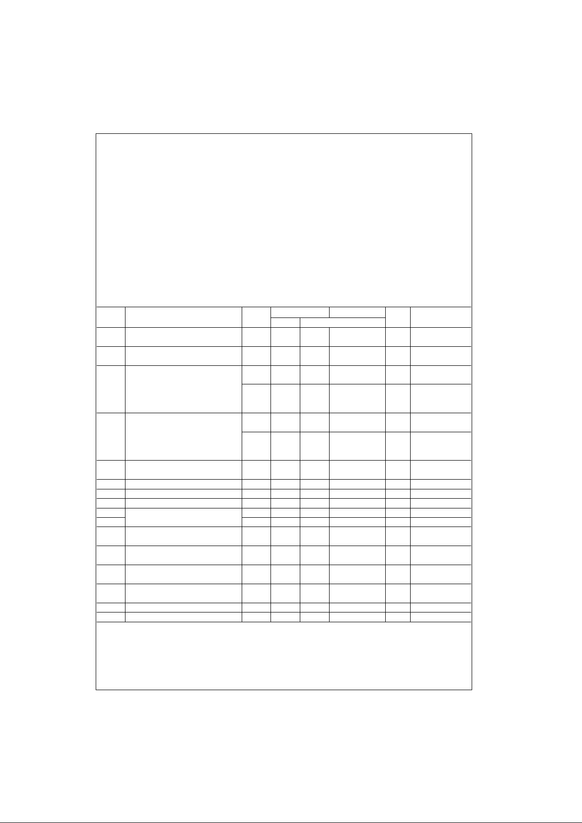
DC Electrical Characteristics
Note 2: All outputs loaded; thresholds associated with output under test.
Note 3: Maximum test duration 2.0 ms; one output loaded at a time.
Note 4: Worst case package.
Note 5: Maximum number of outputs that can switch simultaneously is n. (n − 1) outpu t s are switched LOW and one out put held LOW.
Note 6: Maximum number of outputs that can switch simultaneously is n. (n − 1) outpu t s are switched HIGH and one output held HIGH.
Note 7: Max number of data input s (n ) s w it c hing. (n − 1) input switching 0V to 3V input under test switching 3V to threshold (V
ILD
)
Supply Voltage (VCC) −0.5V to + 7.0V
DC Input Diode Current (I
IK
)
V
I
= −0.5V −20 mA
V
I
= VCC + 0.5V +20 mA
DC Output Diode Current (I
OK
)
V
O
= −0.5V −20 mA
V
O
= VCC +0.5V +20 mA
DC Output Voltage (V
O
) −0.5V to VCC +0.5V
DC Output Source/Sink Current (I
O
) ± 50 mA
DC V
CC
or Ground Current
per Output Pin ± 50 mA
Storage Temperature −65°C to +150°C
Supply Voltage (V
CC
) 4.5V to 5.5V
Input Voltage (V
I
)0V to V
CC
Output Voltage (VO)0V to V
CC
Operating Temperature (TA) −40°C to +85°C
Minimum Input Edge Rate (∆V/∆t) 125 mV/ns
V
IN
from 0.8V to 2.0V
V
CC
@ 4.5V, 5.5V
Symbol Parameter
V
CC
TA = +25°CTA = −40°C to+85°C
Units Conditions
(V) Typ Guaranteed Limits
V
IH
Minimum HIGH 4.5 1.5 2.0 2.0
V
V
OUT
= 0.1V
Input Voltage 5.5 1.5 2.0 2.0 or VCC − 0.1V
V
IL
Maximum LOW 4.5 1.5 0.8 0.8
V
V
OUT
= 0.1V
Input Voltage 5.5 1.5 0.8 0.8 or VCC − 0.1V
V
OH
Minimum HIGH 4.5 4.49 4.4 4.4
VI
OUT
= −50 µA
Output Voltage 5.5 5.49 5.4 5.4
VIN = VIL or V
IH
4.5 3.86 3.76 V IOH = −24 mA
5.5 4.86 4.76 IOH = −24 mA (Note 2)
V
OL
Maximum LOW 4.5 0.001 0.1 0.1
VI
OUT
= 50 µA
Output Voltage 5.5 0.001 0.1 0.1
VIN = VIL or V
IH
4.5 0.36 0.44 V IOL = 24 mA
5.5 0.36 0.44 I
OL
= 24 mA (Note 2)
I
OZT
Maximum I/O
5.5 ±0.5 ±5.0 µA
VI = VIL, V
IH
Leakage Current VO = VCC, GND
I
IN
Maximum Input Leakage Current 5.5 ±0.1 ±1.0 µAVI = VCC, GND
I
CCT
Maximum ICC/Input 5.5 0.6 1.5 mA VI = VCC −2.1V
I
CC
Max Quiescent Supply Current 5.5 8.0 80.0 µAVIN = VCC or GND
I
OLD
Minimum Dynamic 5.5 75 mA V
OLD
= 1.65V Max
I
OHD
Output Current (Note3) 5.5 −75 mA V
OHD
= 3.85V Min
V
OLP
Quiet Output
5.0 0.5 0.8 V
Figure 1, Figure 2
Maximum Dynamic V
OL
(Note 5)(Note 6)
V
OLV
Quiet Output
5.0 −0.5 −0.85 V
Figure 1, Figure 2
Minimum Dynamic V
OL
(Note 5)(Note 6)
V
OHP
Maximum
5.0 VOH + 1.0 VOH + 1.5 V
Figure 1, Figure 2
Overshoot (Note 4)(Note 6)
V
OHV
Minimum
5.0 VOH − 1.0 VOH − 1.8 V
Figure 1, Figure 2
VCC Droop (Note 4)(Note 6)
V
IHD
Minimum HIGH Dynamic Input Voltage Level 5.0 1.7 2.0 V (Note 4)(Note 7)
V
ILD
Maximum LOW Dynamic Input Voltage Level 5.0 1.2 0.8 V (Note 4)(Note 7)
 Loading...