

Fairchild Semiconductor 74ACTQ16240SSCX, 74ACTQ16240SSC, 74ACTQ16240MTDX, 74ACTQ16240MTD, 74ACTQ16240CW Datasheet
May 1991
Revised November 1998
74ACTQ16240 16-Bit Inverting Buffer/Line Driver with 3-STAT E Outputs
© 1999 Fairchild Semiconductor Corporation DS010924.prf www.fairchildsemi.com
74ACTQ16240
16-Bit In verting Buff er/Line Driver with 3-STATE Outputs
General Description
The ACTQ16240 contains sixteen inverting buffers with 3STATE outputs designed to be employed as a memory and
address driver, clock driver, or bus-oriented transmitter/
receiver. The device is nibble controlled. Each nibble has
separate 3-STATE control inputs which can be shorted
together for full 16-bit operation.
The ACTQ16240 utilizes Fairchild’s Quiet Series technology to guarantee quiet output switching and improve
dynamic threshold performa nce. FACT Quiet Series features GTO output control for superior performance.
Features
■ Utilizes Fairchild’s FACT Quiet Series technology
■ Guaranteed simultaneous switching noise level and
dynamic threshold performance
■ Guaranteed pin-to-pin output skew
■ Separate control logic for each byte
■ 16-bit version of the ACTQ240
■ Outputs source/sink 24 mA
■ Additional specs for multiple output switching
■ Output loading specs for both 50 pF and 250 pF loads
Ordering Code:
Device also available in Tape and Reel. Specify by appendin g s uf f ix let t er “X” to the ordering code.
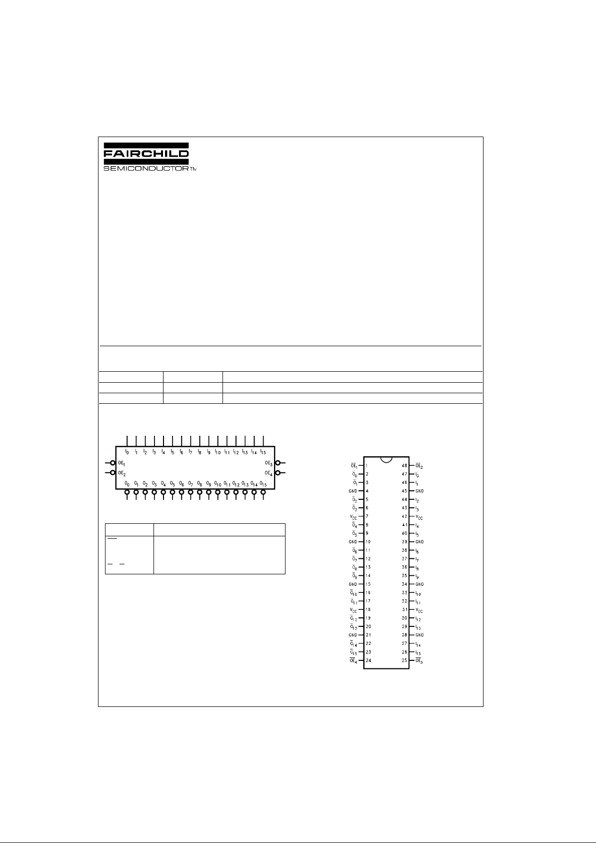
Logic Symbol
Pin Descriptions
Connection Diagram
Pin Assignment
for SSOP and TSSOP
FACT, FACT Quiet Series , Quiet Series, and GTO are trademarks of Fairchild Semiconductor Corporation.
Order Number Package Number Package Description
74ACTQ16240SSC MS48A 48-Lead Small Shrink Outline Package (SSOP), JEDEC MO-118, 0.300” Wide
74ACTQ16240MTD MTD48 48-Lead Thin Shrink Small Outline Package (TSSOP), JEDEC MO-153, 6.1mm Wide
Pin Names Description
OE
n
Output Enable Inputs (Active Low)
I
0–I15
Inputs
O
0–O15
Outputs
www.fairchildsemi.com 2
74ACTQ16240
Truth Tables
H = High Voltage Level
L = Low Voltage Level
X = Immaterial
Z = High Impedance
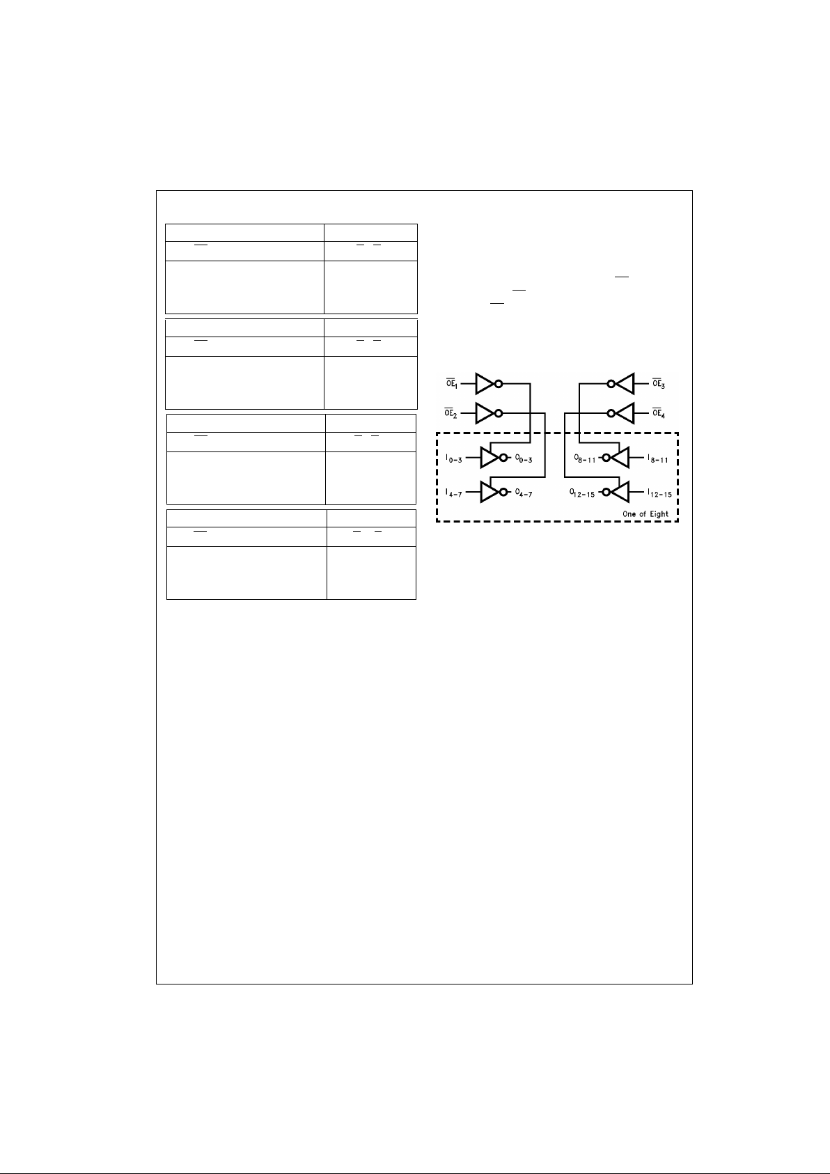
Functional Description
The ACTQ16240 contain s sixteen inver ting buffers with 3STATE standard outputs. The device is n ibble (4 bits) co ntrolled with each nibble fun cti on ing i den ticall y, but independently of the other. The control pins may be shorted
together to obtain ful l 16-bit operation. The 3-STATE outputs are controlled by an Output Enable (OE
n
) input for
each nibble. When OE
n
is LOW, the outputs are in 2-state
mode. When OE
n
is HIGH, the outputs are in the high
impedance mode, but this does not in terfere with entering
new data into the inputs.
Logic Diagram
Inputs Outputs
OE
1
I0–I
3
O0–O
3
LL H
LH L
HX Z
Inputs Outputs
OE
2
I4–I
7
O4–O
7
LL H
LH L
HX Z
Inputs Outputs
OE
3
I8–I
11
O8–O
11
LL H
LH L
HX Z
Inputs Outputs
OE
4
I12–I
15
O12–O
15
LL H
LH L
HX Z
3 www.fairchildsemi.com
74ACTQ16240
Absolute Maximum Ratings(Note 1) Recommended Operating
Conditions
Note 1: Absolute maximum ratings are those values beyond which damage
to the device may occur. The databook specifications should be met, without exception to ensure that the system design is reliable over its power
supply, temperature, and output/in put loading variables. Fairchild does n ot
recommend operat ion of FACT circuits outside databook spe c if ic at ions.
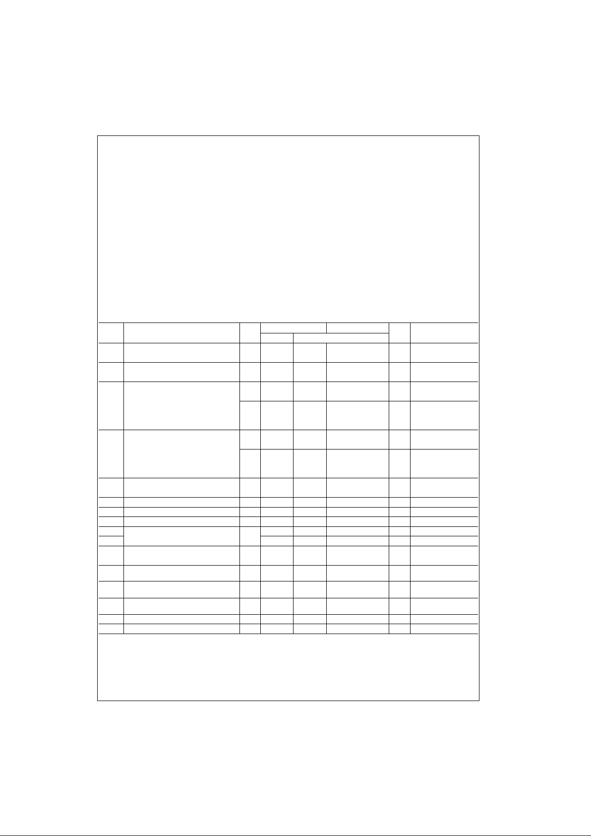
DC Electrical Characteristics
Note 2: All outputs loaded; thresholds associated with output und er t es t .
Note 3: Maximum test duration 2.0 ms; one output loaded at a time.
Note 4: Worst case package.
Note 5: Maximum number of outputs that can switch simultaneously is n. (n − 1) outputs are switched LOW and one output he ld LOW.
Note 6: Maximum number of outputs that can switch simultaneously is n. (n − 1) outputs are switched HIGH and one output held HIGH.
Note 7: Maximum number of data inputs (n) switching . (n − 1) input switching 0V to 3V. Input under test switching 3V t o th reshold (V
ILD
).
Supply Voltage (VCC) −0.5V to +7.0V
DC Input Diode Current (I
IK
)
V
I
= −0.5V −20 mA
V
I
= VCC + 0.5V +20 mA
DC Output Diode Current (I
OK
)
V
O
= −0.5V −20 mA
V
O
= VCC + 0.5V +20 mA
DC Output Voltage (V
O
) −0.5V to VCC + 0.5V
DC Output Source/Sink Current (I
O
) ± 50 mA
DC V
CC
or Ground Current
per Output Pin ± 50 mA
Junction Temperature +140°C
Storage Temperature −65°C to +150°C
Supply Voltage (V
CC
) 4.5V to 5.5V
Input Voltage (V
I
)0V to V
CC
Output Voltage (VO)0V to V
CC
Operating Temperature (TA) −40°C to +85°C
Minimum Input Edge Rate (∆V/∆t) 125 mV/ns
V
IN
from 0.8V to 2.0V
V
CC
@ 4.5V, 5.5V
Symbol Parameter
V
CC
TA = +25°C
TA = −40°C to +85°C
Units Conditions
(V) Typ Guaranteed Limits
V
IH
Minimum High 4.5 1.5 2.0 2.0 V V
OUT
= 0.1V
Input Voltage 5.5 1.5 2.0 2.0 or VCC − 0.1V
V
IL
Maximum Low 4.5 1.5 0.8 0.8 V V
OUT
= 0.1V
Input Voltage 5.5 1.5 0.8 0.8 or VCC − 0.1V
V
OH
Minimum High 4.5 4.49 4.4 4.4 V I
OUT
= −50 µA
Output Voltage 5.5 5.49 5.4 5.4
VIN = VIL or V
IH
4.5 3.86 3.76 V IOH = −24 mA
5.5 4.86 4.76 IOH = −24 mA (Note 2)
V
OL
Maximum Low 4.5 0.001 0.1 0.1 V I
OUT
= 50 µA
Output Voltage 5.5 0.001 0.1 0.1
VIN = VIL or V
IH
4.5 0.36 0.44 V IOL = 24 mA
5.5 0.36 0.44 IOL = 24 mA (Note 2)
I
OZ
Maximum 3-STATE 5.5 ±0.5 ±5.0 µAVI = VIL, V
IH
Leakage Current VO = VCC, GND
I
IN
Maximum Input Leakage Current 5.5 ± 0.1 ± 1.0 µAVI = VCC, GND
I
CCT
Maximum ICC/Input 5.5 0.6 1.5 mA VI = VCC − 2.1V
I
CC
Max Quiescent Supply Current 5.5 8.0 80.0 µAVIN = VCC or GND
I
OLD
Minimum Dynamic 5.5 75 mA V
OLD
= 1.65V Max
I
OHD
Output Current (Note3) −75 mA V
OHD
= 3.85V Min
V
OLP
Quiet Output 5.0 0.5 0.8 V Figure 1Figure 2
Maximum Dynamic V
OL
(Note 5)(Note 6)
V
OLV
Quiet Output Minimum Dynamic V
OL
5.0 −0.5 −1.0 V Figure 1Figure 2
(Note 5)(Note 6)
V
OHP
Maximum Overshoot 5.0 VOH + 1.0 VOH + 1.5 V Figure 1Figure 2
(Note 4)(Note 6)
V
OHV
Minimum VCC Droop 5.0 VOH − 1.0 VOH − 1.8 V Figure 1Figure 2
(Note 4)(Note 6)
V
IHD
Minimum High Dynamic Input Voltage Level 5.0 1.7 2.0 V (Note 4)(Note 7)
V
ILD
Maximum Low Dynamic Input Voltage Level 5.0 1.2 0.8 V (Note 4)(Note 7)
 Loading...