Fairchild Semiconductor 74ACT563SC, 74ACT563PC, 74ACT563CW Datasheet

November 1988
Revised December 1998
74ACT563 Octal Latc h with 3-STATE Outputs
© 1999 Fairchild Semiconductor Corporation DS009970.prf www.fairchildsemi.com
74ACT563
Octal Latch with 3-STATE Outputs
General Description
The ACT563 is a high-speed oct al latch w ith buffered common Latch Enable (LE) and buffered common Output
Enable (OE
) inputs.
The ACT563 device is functionally identical to the ACT573,
but with inverted outputs.
Features
■ ICC and IOZ reduced by 50%
■ Inputs and outputs on opposit e sides of package allow
easy interface with microprocessors
■ Useful as input or output port for microprocessors
■ Functionally identi cal to ACT573 but with inverted out-
puts
■ Outputs source/sink 24 mA
■ ACT563 has TTL-compatible inputs
Ordering Code:
Device also available in Tape and Reel. Specify by appendin g s uf f ix let t er “X” to the ordering code.
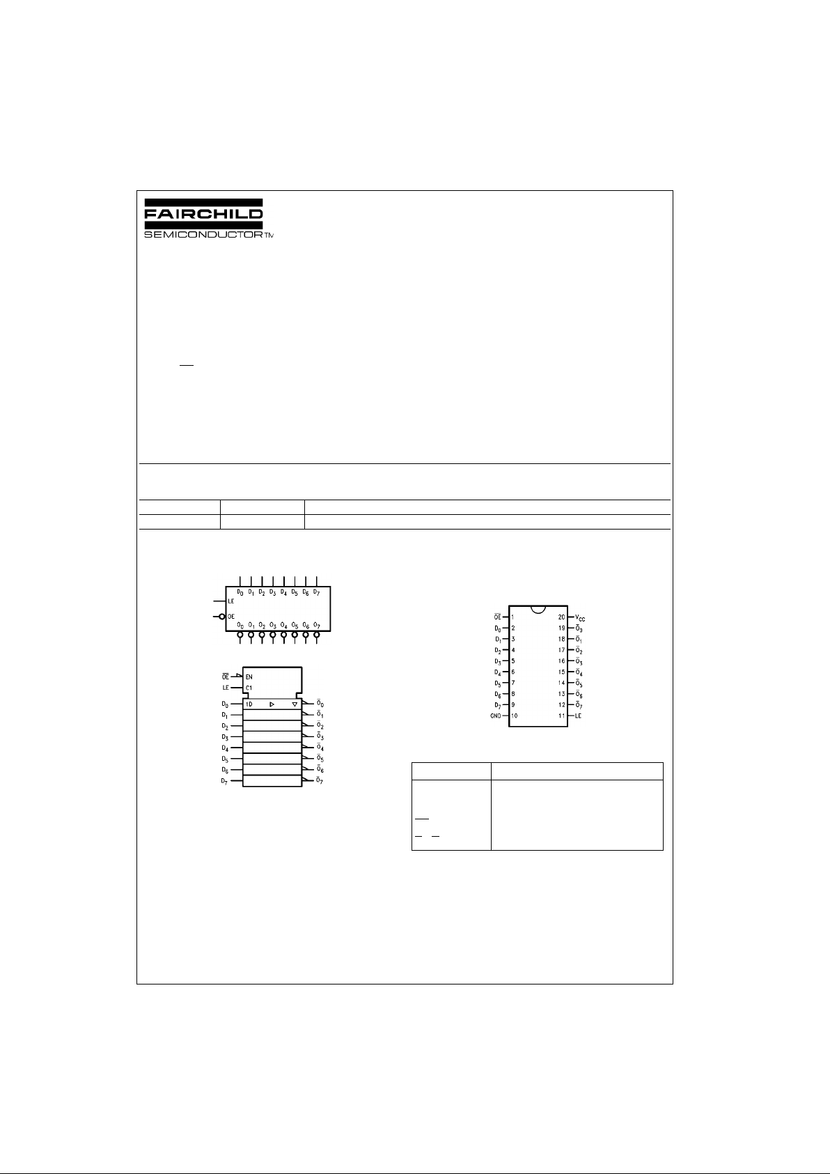
Logic Symbols
IEEE/IEC
Connection Diagram
Pin Assignment
for SOIC
Pin Descriptions
FACT is a tra demark of Fairchild Semiconductor Corporatio n.
Order Number Package Number Package Description
74ACT563SC M20B 20-Lead Small Outline Integrated Circuit (SOIC), JEDEC MS-013, 0.300” Wide Body
Pin Names Description
D
0–D7
Data Inputs
LE Latch Enable Input
OE
3-STATE Output Enable Input
O
0–O7
3-ST ATE Latch Outputs

www.fairchildsemi.com 2
74ACT563
Functional Description
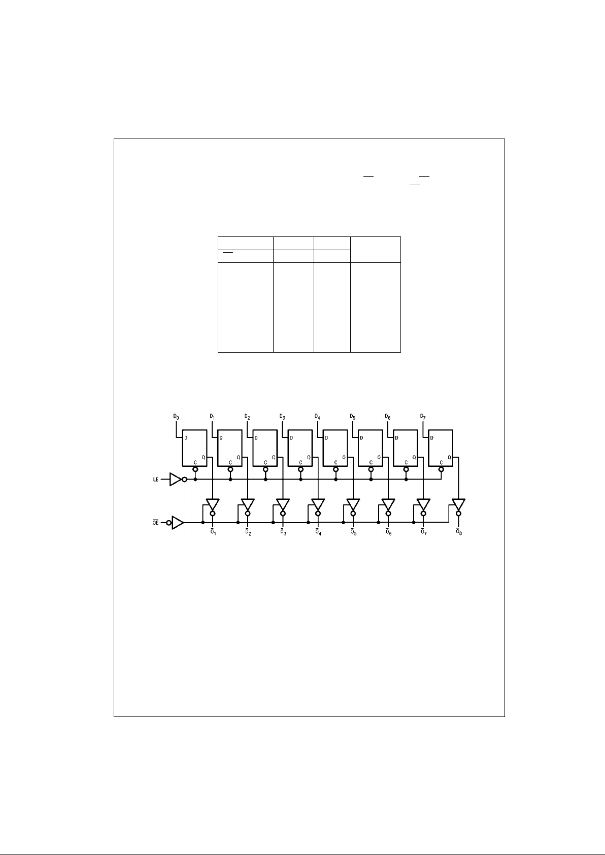
The ACT563 contains eight D-type latches with 3-STATE
complementar y o utp uts. Wh en the Latc h Enabl e (L E) i np ut
is HIGH, data on the D
n
inputs enters the latches. In this
condition the latches are transparent, i.e., a latch output will
change state each time its D input changes. When LE is
LOW the latches store the information that was present on
the D inputs at setup time preceding the HIGH-to-LOW
transition of LE. The 3-STATE buffers are controlled by the
Output Enable (OE) input. When OE is LOW, the buffers
are in the bi-state m od e. When OE
is HIGH the buffers are
in the high impedance mode but that does not interfere with
entering new data into the latches.
Function Table
H = HIGH Voltage Level
L = LOW V oltage Level
X = Immaterial
Z = High Impedance
NC = No Change
Logic Diagram
Please note that this diagram is provided only for the und ers t anding of logic operations and should not be used to es t im at e propagation delays.
Inputs Internal Outputs Function
OE
LE D Q O
H X X X Z High-Z
H H L H Z High-Z
H H H L Z High-Z
H L X NC Z Latched
L H L H H Transparent
L H H L L Transparent
L L X NC NC Latched
 Loading...