

Fairchild Semiconductor 74ACT541SCX, 74ACT541SC, 74ACT541PC, 74ACT541MTCX, 74ACT541MTC Datasheet
November 1988
Revised October 1999
74AC541 • 74ACT541
Octal Buffer/Line Driver with 3-STATE Outputs
74AC541 • 74ACT541 Octal Buffer/Line Driver with 3-STATE Outputs
General Description
The 74AC541 and 74 ACT541 are octal buffer/l ine drivers
designed to be em ployed as mem ory a nd ad dress d rive rs,
clock drivers and bus oriented transmitter/receivers.
These devices are similar in fu nction to the 74AC244 a nd
74ACTC244 while providing flow-through architecture
(inputs on opposite side from outputs). This pinout arrangement makes these devices esp ecially useful as an outp ut
port for microprocessors, allowing ease of layout and
greater PC board density.
Features
■ ICC and IOZ reduced by 50%
■ 3-STATE outputs
■ Inputs and outputs opposite side of package, allowing
easier interface to microprocessors
■ Output source/sink 24 mA
■ 74AC541 is a non-inverting option of the 74AC540
■ 74ACT541 has TTL-compatible inputs
Ordering Code:
Order Number Package Number Package Description
74AC541SC M20B 20-Lead Small Outline Integrated Circuit (SOIC), JEDEC MS-013, 0.300” Wide Body
74AC541SJ M20D 20-Lead Small Outline Package (SOP), EIAJ TYPE II, 5.3mm Wide
74AC541MTC MTC20 20-Lead Thin Shrink Small Outline Package (TSSOP), JEDEC MO-153, 4.4mm Wide
74AC541PC N20A 20-Lead Plastic Dual-In-Line Package (PDIP), JEDEC MS-001, 0.300” Wide
74ACT541SC M20B 20-Lead Small Outline Integrated Circuit (SOIC), JEDEC MS-013, 0.300” Wide Body
74ACT541MTC MTC20 20-Lead Thin Shrink Small Outline Package (TSSOP), JEDEC MO-153, 4.4mm Wide
74ACT541PC N20A 20-Lead Plastic Dual-In-Line Package (PDIP), JEDEC MS-001, 0.300” Wide
Device also available in Tape and Reel. Specify by appending s uffix let te r “X” to the ordering code .
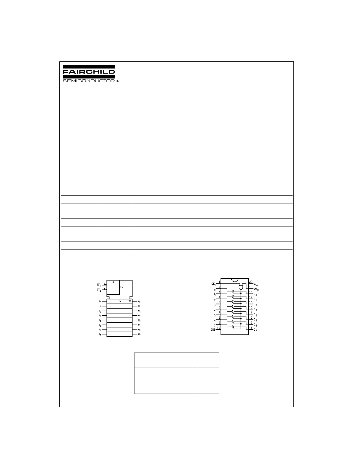
Logic Symbol
IEEE/IEC
Connection Diagram
Truth Table
Inputs
OE
L L HH
H X XZ
X H XZ
FACT is a trade m ark of F airchild Semicondu ctor Corporation.
© 1999 Fairchild Semiconductor Corporation DS009967 www.fairchildsemi.com
H = HIGH Voltage Level X = Immaterial L = LOW Voltage Level Z = High Impedance
L L LL
OE
1
2
Outputs
I
Absolute Maximum Ratings(Note 1) Recommended Operating
Supply Voltage (VCC) −0.5V to +7.0V
DC Input Diode Current (I
= −0.5V −20 mA
V
I
= VCC + 0.5V +20 mA
V
I
DC Input Voltage (V
DC Output Diode Current (I
= −0.5V −20 mA
V
O
= VCC + 0.5V +20 mA
V
74AC541 • 74ACT541
O
DC Output Voltage (V
)
IK
) −0.5V to VCC + 0.5V
I
)
OK
) −0.5V to VCC + 0.5V
O
DC Output Source
or Sink Current (I
DC V
or Ground Current
CC
per Output Pin (I
Storage Temperature (T
Junction Temperature (T
) ± 50 mA
O
or I
CC
) ± 50 mA
GND
) −65°C to +150°C
STG
)
J
PDIP 140°C
Conditions
Supply Voltage (V
AC 2.0V to 6.0V
ACT 4.5V to 5.5V
Input Voltage (V
Output Voltage (VO) 0V to V
Operating Temperature (TA) −40°C to +85°C
Minimum Input Edge Rate (∆V/∆t) 125 mV/ns
from 30% to 70% of V
AC: V
IN
VCC @ 3.3V, 4.5V, 5.5V
ACT:V
IN
V
CC
Note 1: Absolute maximum ratings are those values beyond which damage to the device may occu r. The databook specificati ons should be met,
without exception, t o ensure that the system design is reliab le over its
power supply, temperature, an d output/input loading variables. Fairc hild
does not recommend operation of FACT circuits outside databook specifications.
)
CC
) 0V to V
I
from 0.8V to 2.0V
@ 4.5V, 5.5V
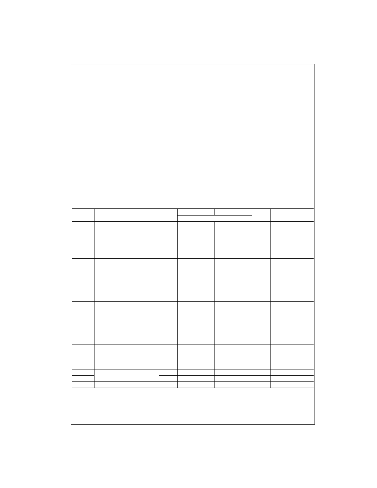
DC Electrical Characteristics for AC
CC
CC
CC
V
Symbol Parameter
V
IH
V
IL
V
OH
V
OL
IIN (Note 4) Maximum Input Leakage Current 5.5 ± 0.1 ± 1.0 µA VI = V
I
OZ
I
OLD
I
OHD
ICC (Note 4) Maximum Quiescent Supply Current 5.5 4.0 40.0 µAVIN = VCC or GND
Note 2: All outputs loaded; thresholds on input associated wit h output under test.
Note 3: Maximum te st duration 2.0 ms, one ou t put loaded at a time.
Note 4: I
Minimum HIGH Level 3.0 1.5 2.1 2.1
Input Voltage 4.5 2.25 3.15 3.15 or VCC − 0.1V
Maximum LOW Level 3.0 1.5 0.9 0.9
Input Voltage 4.5 2.25 1.35 1.35 or VCC − 0.1V
Minimum HIGH Level 3.0 2.99 2.9 2.9
Maximum LOW Level 3.0 0.002 0.1 0.1
Output Voltage 4.5 0.001 0.1 0.1 I
Maximum 3-STATE
Leakage Current 5.5 ±0.25 ±2.5 VI = VCC, GND
Minimum Dynamic 5.5 75 mA V
Output Current (Note 3) 5.5 −75 mA V
and ICC @ 3.0V are guaranteed to be less than or equal to the respective limit @ 5. 5V VCC.
IN
CC
(V) Typ Guaranteed Limits
5.5 2.75 3.85 3.85
5.5 2.75 1.65 1.65
5.5 5.49 5.4 5.4
3.0 2.56 2.46 IOH = −12 mA
4.5 3.86 3.76 IOH = −24 mA
5.5 4.86 4.76 IOH = −24 mA (Note 2)
5.5 0.001 0.1 0.1
3.0 0.36 0.44 IOL = 12 mA
4.5 0.36 0.44 IOL = 24 mA
5.5 0.36 0.44 IOL = 24 mA (Note 2)
TA = +25°CTA = −40°C to +85°C
Units Conditions
V
= 0.1V
OUT
V
V
= 0.1V
OUT
V
VOutput Voltage 4.5 4.49 4.4 4.4 I
V
V
V
µA
= −50 µA
OUT
VIN = VIL or V
= 50 µA
OUT
VIN = VIL or V
, GND
CC
VI (OE) = V
VO = VCC, GND
= 1.65V Max
OLD
= 3.85V Min
OHD
IL
IH
IH
, V
IH
www.fairchildsemi.com 2
AC Electrical Characteristics for AC
V
CC
Symbol Parameter (V)
(Note 5) Min Typ Max Min Max
t
PLH
Propagation Delay 3.3 2.0 5.5 8.0 1.5 9.0
Data to Output 5.0 1.5 4.0 6.0 1.0 6.5
t
PHL
Propagation Delay 3.3 2.0 5.5 8.0 1.5 8.5
Data to Output 5.0 1.5 4.0 6.0 1.0 6.5
t
PZH
Output Enable Time 3.3 3.0 8.0 11.5 3.0 12.5
5.0 2.0 6.0 8.5 1.5 9.5
t
PZL
Output Enable Time 3.3 2.5 7.0 10.0 2.5 11.5
5.0 1.5 5.5 7.5 1.0 8.5
t
PHZ
Output Disable Time 3.3 3.5 9.0 12.5 2.5 14.0
5.0 2.0 7.0 9.5 1.0 10.5
t
PLZ
Output Disable Time 3.3 2.5 6.5 9.5 2.0 10.5
5.0 2.0 5.5 7.5 1.0 8.5
Note 5: Voltage Range 3.3 is 3.3V ± 0.3V
Voltage Range 5.0 is 5.0V ± 0.5V
DC Electrical Characteristics for ACT
TA = +25°CT
= 50 pF CL = 50 pF
C
L
= −40°C to +85°C
A
74AC541 • 74ACT541
Units
ns
ns
ns
ns
ns
ns
Symbol Parameter
V
IH
Minimum HIGH Level 4.5 1.5 2.0 2.0
V
CC
(V) Typ Guaranteed Limits
TA = +25°CT
Input Voltage 5.5 1.5 2.0 2.0 or V
V
IL
Maximum LOW Level 4.5 1.5 0.8 0.8
Input Voltage 5.5 1.5 0.8 0.8 or VCC − 0.1V
V
OH
Minimum HIGH Level 3.0 2.99 2.9 2.9
Output Voltage 4.5 4.49 4.4 4.4
4.5 3.86 3.76
5.5 4.86 4.76 IOH = −24 mA
V
OL
Maximum LOW Level 3.0 0.002 0.1 0.1
Output Voltage 4.5 0.001 0.1 0.1
4.5 0.36 0.44
5.5 0.36 0.44 IOH = 24 mA
I
IN
I
OZ
I
CCT
I
OLD
I
OHD
I
CC
Note 6: All outputs loaded; thresholds on input associated with ou t put under test.
Note 7: Maximum test duration 2.0 ms, one output loaded at a time.
Maximum Input
Leakage Current
Maximum 3-STATE
Leakage Current VO = VCC, GND
5.5 ± 0.1 ± 1.0 µA VI = V
5.5 ±0.25 ±2.5 µA
Maximum ICC/Input 5.5 0.6 1.5 mA VI = VCC − 2.1V
Minimum Dynamic 5.5 75 mA V
Output Current (Note 7) 5.5 −75 mA V
Maximum Quiescent
Supply Current
5.5 4.0 40.0 µAVIN = VCC or GND
= −40°C to +85°C
A
Units Conditions
V
= 0.1V
OUT
V
V
VI
− 0.1V
CC
V
= 0.1V
OUT
= −50 µA
OUT
VIN = VIL or V
IH
V
IOH = −24 mA (Note 6)
VI
= 50 µA
OUT
VIN = VIL or V
IH
V
IOH = 24 mA (Note 6)
, GND
CC
VI = V
, V
IL
IH
= 1.65V Max
OLD
= 3.85V Min
OHD
3 www.fairchildsemi.com
 Loading...