

Fairchild Semiconductor 74ABT16500CSSCX, 74ABT16500CSSC, 74ABT16500CMTDX, 74ABT16500CMTD Datasheet
April 1993
Revised January 1999
74ABT16500 18-Bit Universal Bus Transceivers with 3-STATE Outputs
© 1999 Fairchild Semiconductor Corporation DS011581.prf www.fairchildsemi.com
74ABT16500
18-Bit Universal Bus Transceivers with 3-STATE Outputs
General Description
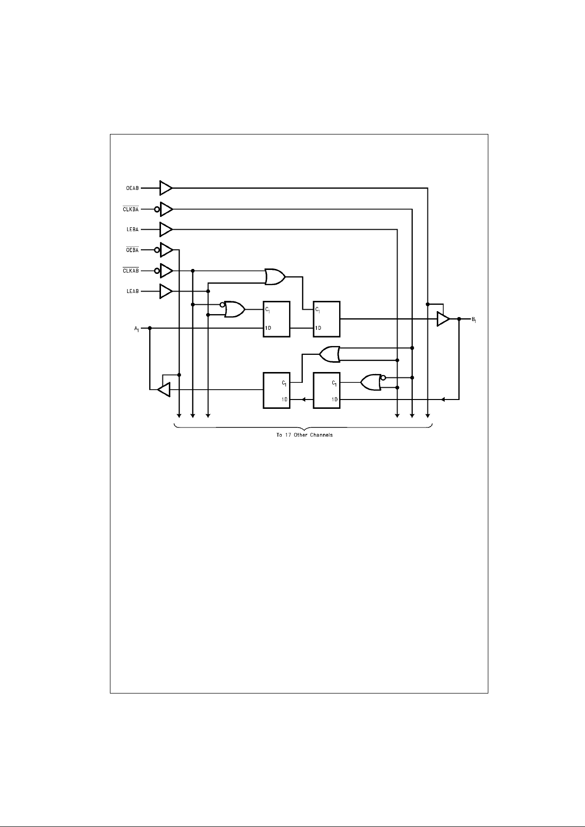
The ABT16500 18-bit u niversal bus transceiver combines
D-type latches and D-type flip-flops to allow data flow in
transparent, latched, and clocked modes.
Data flow in each direction is contr olled by output-enable
(OEAB and OEBA
), latch-enable (LEAB and LEBA), and
clock (CLKAB
and CLKBA) inputs. For A-to-B data flow, the
device operates in the transparent mode when LEAB is
HIGH. When LEAB is LOW, the A data is latched if CLKAB
is held at a HIGH or LOW logic level. If LEAB is LOW, the A
bus data is stored in the latch/flip-flop on the HIGH-to-LOW
transition of CLKAB
. Output-enable OEAB is active-high.
When OEAB is HIGH, the outputs are active. When OEAB
is LOW, the outputs are in the high-impedance state.
Data flow for B to A is similar to tha t of A to B but uses
OEBA
, LEBA, and CLKBA. The output enables ar e com-
plementary (OEAB is active HIGH and OEBA
is active
LOW).
To ensure the high-imp edance state during power up or
power down, OE should be tied to GN D t hr o ug h a pulldown
resistor; the minimum value of the resistor is determined by
the current-sourcing capability of the driver.
Features
■ Combines D-Type latches and D-Type flip-flops for
operation in transparent, latched, or clocked mode
■ Flow-through architecture optimizes PCB layout
■ Guaranteed latch-up protection
■ High impedance glitch free bus loading during entire
power up and power down cycle
■ Non-destructive hot insertion capability
Ordering Code:
Devices also available in Tape and Reel. Specify by appending the letter suffix “X” to t he ordering code.
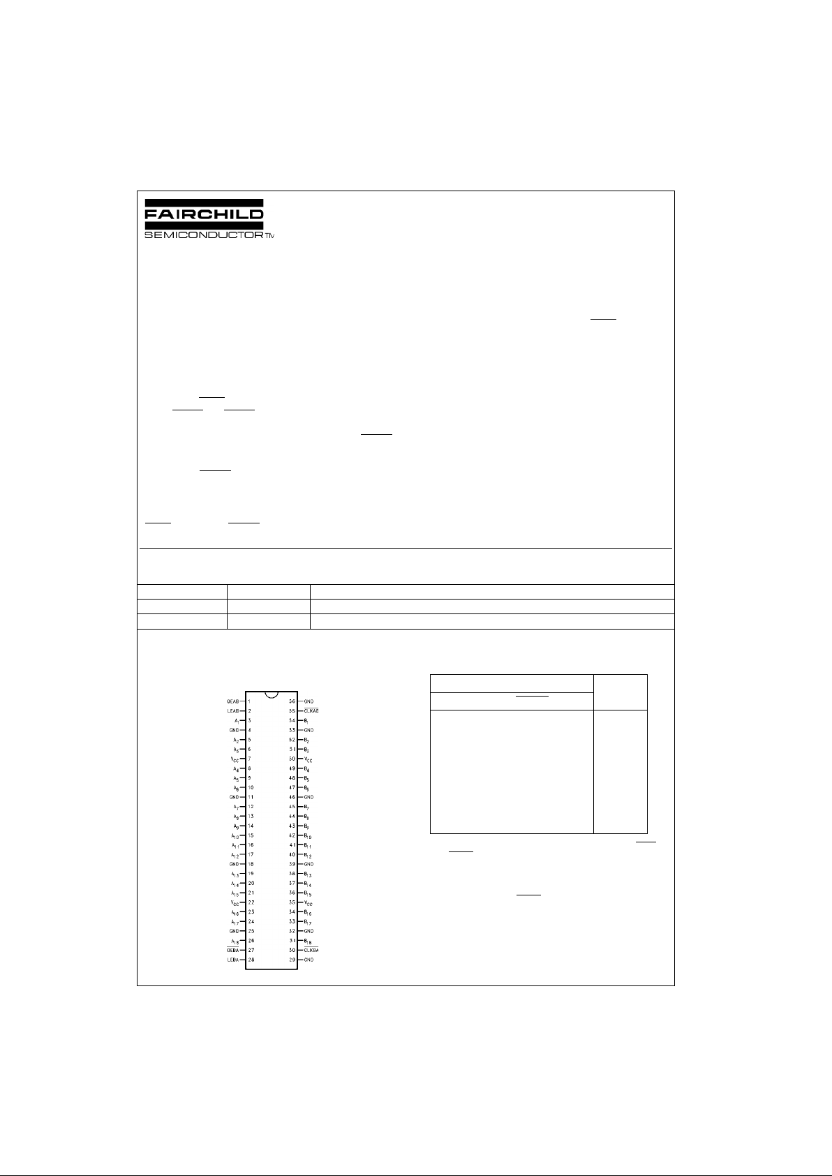
Connection Diagram
Pin Assign ment for SSOP
Function Table (Note 1)
Note 1: A-to-B data flow is s hown: B-to-A flow is similar but use s OEBA,
LEBA, and CLKBA
.
Note 2: Output level before the indicated s teady-state input conditions
were established.
Note 3: Output level before the indicated s teady-state input conditions
were established, provid ed t hat CLKAB
was LOW before LEAB went LOW.
Order Number Package Number Package Description
74ABT16500CSSC MS56A 56-Lead Shrink Small Outline Package (SSOP), JEDEC MO-118, 0.300” Wide
74ABT16500CMTD MTD56 56-Lead Thin Shrink Small Outline Package (TSSOP), JEDEC MO-153, 6.1mm Wide
Inputs Output
OEAB LEAB CLKAB
AB
LXXX Z
HHXL L
HHXH H
HL↓ LL
HL↓ HH
HLHXB
0
(Note 2)
HLLXB
0
(Note 3)
www.fairchildsemi.com 2
74ABT16500
Logic Diagram
3 www.fairchildsemi.com
74ABT16500
Absolute Maximum Ratings(Note 4)
Recommended Operating
Conditions
Note 4: Absolute maximum ratings are values beyond which the device
may be damaged or have its useful life impaired. Functional operation
under these condit ions is not implied.
Note 5: Either voltage limit or current limi t is s uf f ic ient to protect inputs.
DC Electrical Characteristics
Note 6: Guaranteed, but not tested.
Storage Temperature −65°C to +150°C
Ambient Temperature under Bias −55°C to +125°C
Junction Temperature under Bias −55°C to +150°C
V
CC
Pin Potential to
Ground Pin −0.5V to +7.0V
Input Voltage (Note 5) −0.5V to +7.0V
Input Current (Note 5) −30 mA to +5.0 mA
Voltage Applied to Any Output
in the Disabled or
Power-off State −0.5V to 5.5V
in the HIGH State −0.5V to V
CC
Current Applied to Output
in LOW State (Max) twice the rated I
OL
(mA)
DC Latchup Source Current −500 mA
Over Voltage Latchup (I/O) 10V
Free Air Ambient Temperature −40°C to +85°C
Supply Voltage +4.5V to +5.5V
Minimum Input Edge Rate (∆V/∆t)
Data Input 50 mV/ns
Enable Input 20 mV/ns
Symbol Parameter Min Typ Max Units
V
CC
Conditions
V
IH
Input HIGH Voltage 2.0 V Recognized HIGH Signal
V
IL
Input LOW Vo ltage 0.8 V Recognized LOW Signal
V
CD
Input Clamp Diode Voltage −1.2 V Min IIN = −18 mA
V
OH
Output HIGH Voltage 2.5 V Min IOH = −3 mA
2.0 V Min IOH = −32 mA
V
OL
Output LOW Voltage 0.55 V Min IOL = 64 mA
I
IH
Input HIGH Current 1 µAMaxVIN = 2.7V (Note 6)
1V
IN
= V
CC
I
BVI
Input HIGH Current Breakdown Test 7 µAMaxVIN = 7.0V
I
IL
Input LOW Current −1 µAMaxVIN = 0.5V (Note 6)
−1V
IN
= 0.0V
V
ID
Input Leakage Test 4.75 V 0.0 IID = 1.9 µA
All Other Pins Grounded
IIH + Output Leakage Current
10 µA0 − 5.5V
V
OUT
= 2.7V; OE, OE = 2.0V
I
OZH
IIL + Output Leakage Current
−10 µA0 − 5.5V
V
OUT
= 0.5V; OE, OE = 2.0V
I
OZL
I
OS
Output Short-Circuit Current −100 −275 mA Max V
OUT
= 0V
I
CEX
Output HIGH Leakage Current 50 µAMaxV
OUT
= V
CC
I
ZZ
Bus Drainage Test 100 µA0.0V
OUT
= 5.5V; All Others GND
I
CCH
Power Supply Current 1.0 mA Max All Outputs HIGH
I
CCL
Power Supply Current 68 µA Max An or Bn Outputs Low
I
CCZ
Power Supply Current
1.0 mA Max
OEn = VCC,
All Others at VCC or GND
I
CCT
Additional ICC/Input 2.5 mA Max VI = VCC − 2.1V
All Others at VCC or GND
I
CCD
Dynamic I
CC
No Load mA/ Max Outputs Open
(Note 6) 0.23 MHz Transparent Mode
One Bit Toggling, 50% Duty Cycle
 Loading...