

Fairchild Semiconductor 74ABT16374CSSCX, 74ABT16374CMTDX, 74ABT16374CMTD Datasheet
© 1999 Fairchild Semiconductor Corporation DS011668 www.fairchildsemi.com
March 1994
Revised November 1999
74ABT16374 16-Bit D-Type Flip-Flop with 3-STATE Outputs
74ABT16374
16-Bit D-Type Flip-Flop with 3-STATE Outputs
General Description
The ABT16374 contains sixteen non-inverting D-ty pe flipflops with 3-STATE outputs and is intended for bus oriented
applications. The device is byte controlled. A buffered clock
(CP) and Output E nable (OE
) are common to each byte
and can be shorted together for full 16-bit operation.
Features
■ Separate control logic for each byte
■ 16-bit version of the ABT374
■ Edge-triggered D-type inputs
■ Buffered Positive edge-triggered clock
■ High impedance glitch free bus loading during entire
power up and power down cycle
■ Non-destructive hot insertion capability
■ Guaranteed latch-up protection
Ordering Code:
Devices also availab le in Tape and Reel. Specify by appending suffix letter “X” to the ordering code.
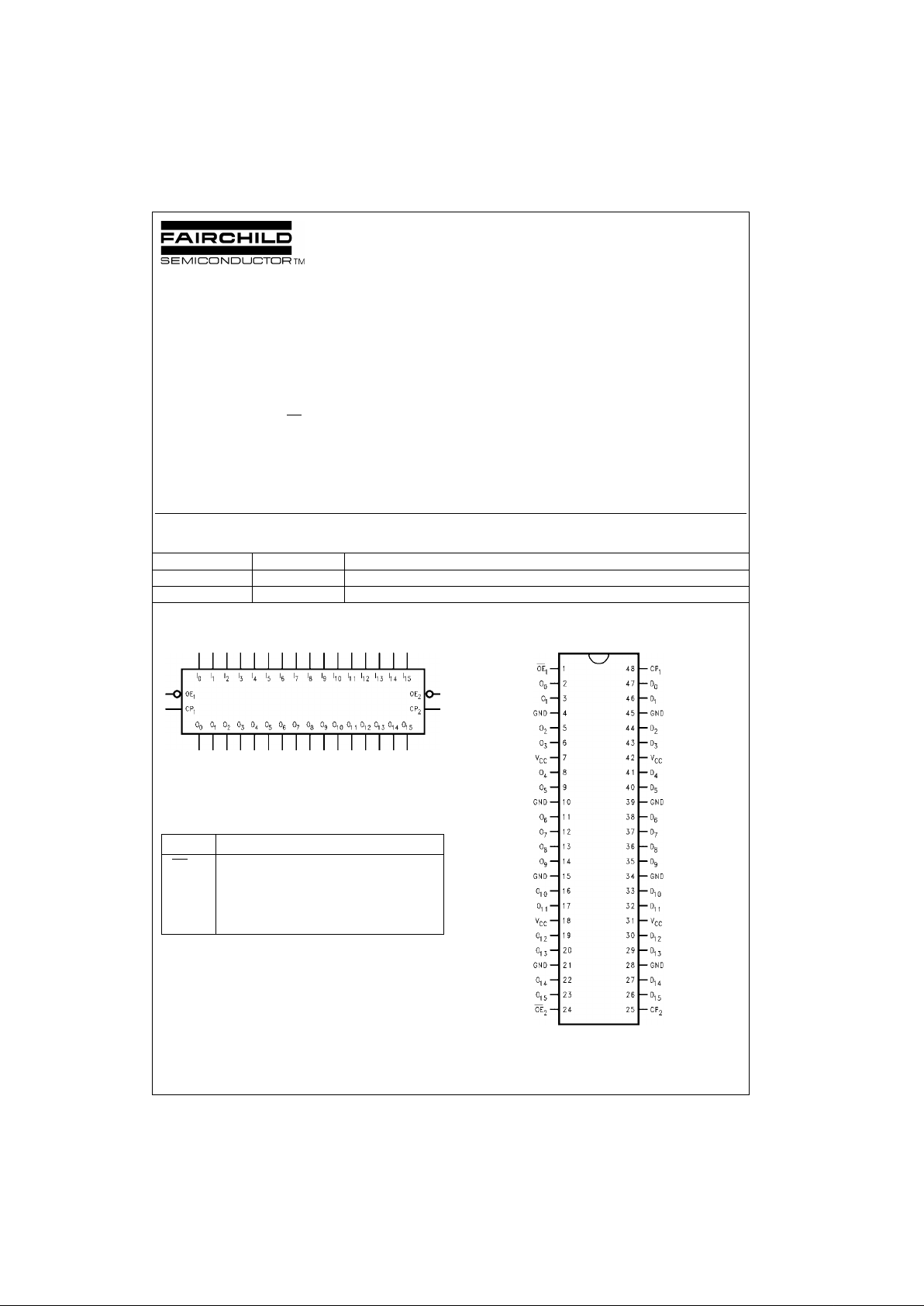
Logic Symbol
Pin Descriptions
Connection Diagram
Order Number Package Number Package Description
74ABT16374CSSC MS48A 48-Lead Small Shrink Outline Package (SSOP), JEDEC MO-118, 0.300” Wide
74ABT16374CMTD MTD48 48-Lead Thin Shrink Small Outline Package (TSSOP), JEDEC MO-153, 6.1mm Wide
Pin Name Description
OE
n
3-STATE Output Enable Input (Active LOW)
CP
n
Clock Pulse Input (Active Rising Edge)
D
0–D15
Data Inputs
O
0–O15
3-STATE Outputs
www.fairchildsemi.com 2
74ABT16374
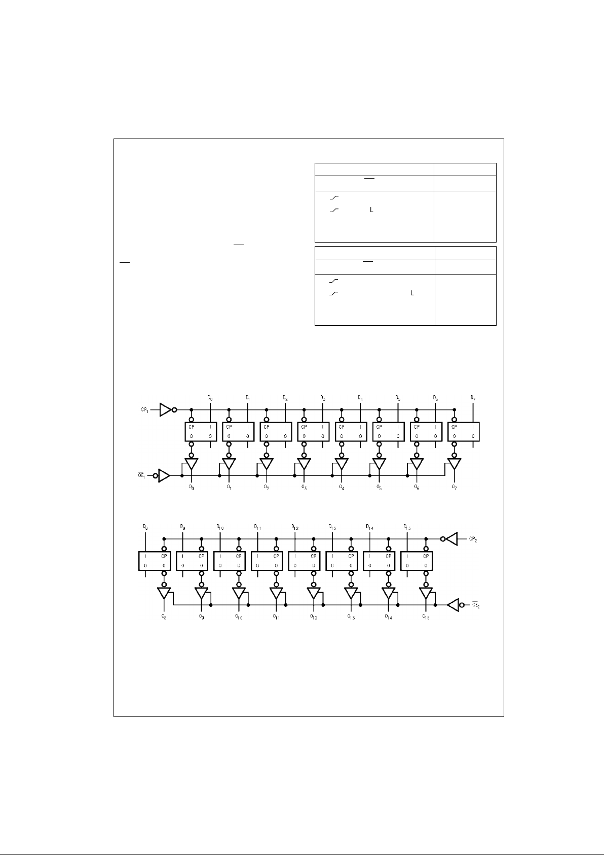
Functional Description
The ABT16374 consists o f si xte en edg e-t rigg er ed f lip -flo ps
with individual D-type inputs and 3-STATE true outputs.
The device is byte controlled with each byte functionin g
identically, but independent of the ot her. The control pins
can be shorted together to obtain full 16-bit operation.
Each byte has a buffered clock and buffered Output Enable
common to all flip-flo ps within that byte. The description
which follows applies to each byte. Each flip-flop will store
the state of their individual D inputs that meet the setup and
hold time requirem ents on the LOW-to-HIG H Clock (CP
n
)
transition. With the Output Ena ble (OE
n
) LOW, the con-
tents of the flip-flops a re available at the outputs. When
OE
n
is HIGH, the outputs go to the high imped ance state.
Operation of the OE
n
input does not affect the st ate of the
flip-flops.
Tr uth Tables
H = HIGH Voltage Level
L = LOW Voltage Level
X = Immaterial
Z = High Impedance
Logic Diagrams
Byte 1 (0:7)
Byte 2 (8:15)
Inputs Outputs
CP
1
OE
1
D0–D
7
O0–O
7
L H H
L L L
L L X (Previous)
X H X Z
Inputs Outputs
CP
2
OE
2
D8–D
15
O8–O
15
L H H
L L L
L L X (Previous)
X H X Z
 Loading...