

Fairchild Semiconductor 74ABT16244CSSCX, 74ABT16244CSSC, 74ABT16244CMTDX, 74ABT16244CMTD Datasheet
© 1999 Fairchild Semiconductor Corporation DS010985 www.fairchildsemi.com
April 1992
Revised November 1999
74ABT16244 16-Bit Buffer/Line Driver with 3-STATE Outputs
74ABT16244
16-Bit Buffer/Line Driver with 3-STATE Outputs
General Description
The ABT16244 contai ns sixteen n on-invertin g buffers with
3-STATE ou tputs designed to be employed as a memo ry
and address driver, clock driver, or bus oriented transmitter/receiver. The device is nibble cont rolled. Individual 3STATE contro l inputs can be shorted t ogether for 8-bit or
16-bit operation.
Features
■ Separate control logic for each nibble
■ 16-bit version of the ABT244
■ Outputs sink capability of 64 mA, source capability of
32 mA
■ Guaranteed output skew
■ Guaranteed multiple output switching specifications
■ Output switching specified for both 50 pF and
250 pF loads
■ Guaranteed simultaneous switching noise level and
dynamic threshold performan ce
■ Guarante ed latchup protection
■ High impedance glitch free bus loading during entire
power up and power down cycle
■ Non-destructive hot insertion capability
Ordering Code:
Devices are also avai lable in Tape and Reel. Specify by appending the suffix letter “X” to the ordering code.
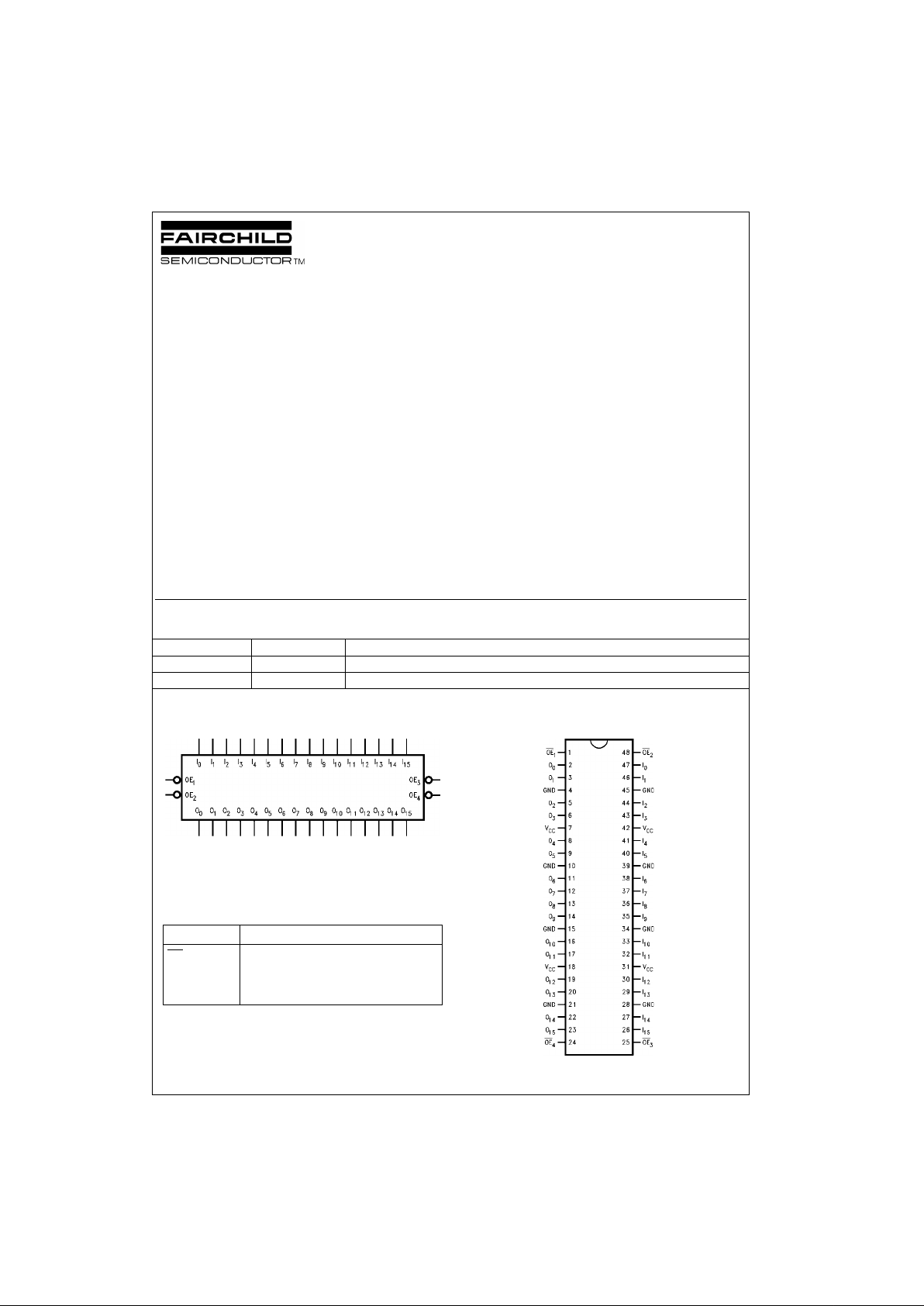
Logic Symbol
Pin Descriptions
Connection Diagram
Order Number Package Number Package Description
74ABT16244CSSC MS48A 48-Lead Small Shrink Outline Package (SSOP), JEDEC MO-118, 0.300” Wide
74ABT16244CMTD MTD48 48-Lead Thin Shrink Small Outline Package (TSSOP), JEDEC MO-153, 6.1mm Wide
Pin Names Description
OE
n
Output Enable Inputs (Active LOW)
I
0–I15
Inputs
O
0–O15
Outputs
www.fairchildsemi.com 2
74ABT16244
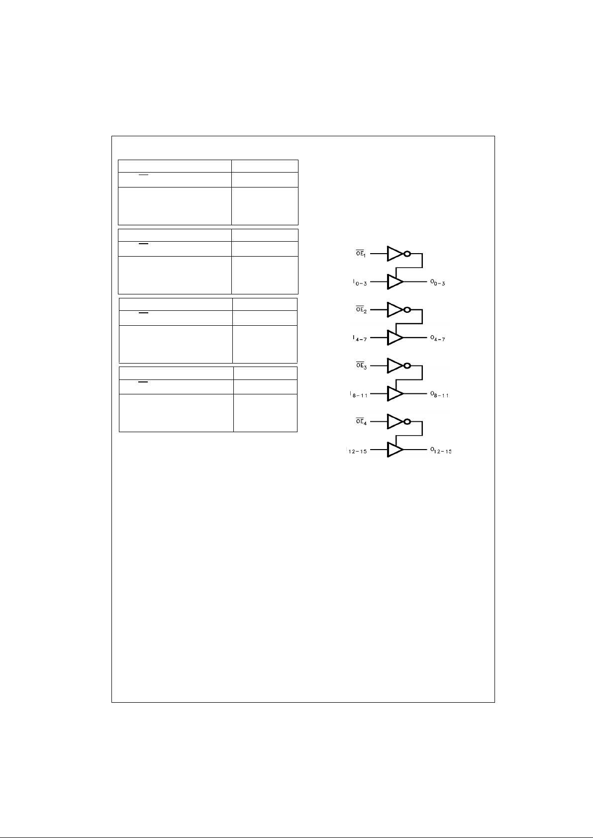
Truth Tables
H = HIGH Voltage Level
L = LOW Voltage Level
X = Immaterial
Z = High Impedance
Functional Description
The ABT16244 contains sixtee n non-inverting buffers with
3-STATE outp uts. The device is nibble (4 bits) contr olled
with each nibble functi oning ident ically, but independent of
the other. The control pins can be shorted together to
obtain full 16-bit operation.
Logic Diagram
Inputs Outputs
OE
1
I0–I
3
O0–O
3
L L L
L H H
H X Z
Inputs Outputs
OE
2
I4–I
7
O4–O
7
L L L
L H H
H X Z
Inputs Outputs
OE
3
I8–I
11
O8–O
11
L L L
L H H
H X Z
Inputs Outputs
OE
4
I12–I
15
O12–O
15
L L L
L H H
H X Z
3 www.fairchildsemi.com
74ABT16244
Absolute Maximum Ratings(Note 1) Recommended Operating
Conditions
Note 1: Absolute maximum ratings are values beyond which the device
may be damaged or have its useful life impaired . Functional operation
under these conditions is not implied.
Note 2: Either voltage lim it or c urrent limit is sufficient to pro te c t in puts.
DC Electrical Characteristics
Note 3: Guaranteed but not tested.
Storage Temperature −65°C to +150°C
Ambient Temperature under Bias −55°C to +125°C
Junction Temperature under Bias −55°C to +150°C
V
CC
Pin Potential to Ground Pin −0.5V to +7.0V
Input Voltage (Note 2) −0.5V to +7.0V
Input Current (Note 2) −30 mA to +5.0 mA
Voltage Applied to Any Output
in the Disabled or
Power-Off State −0.5V to 5.5V
in the HIGH State −0.5V to V
CC
Current Applied to Output
in LOW State (Max) twice the rated I
OL
(mA)
DC Latchup Source Current −500 mA
Over Voltage Latchup (I/O) 10V
Free Air Ambient Temperature −40°C to +85°C
Supply Voltage +4.5V to +5.5V
Minimum Input Edge Rate (∆V/∆t)
Data Input 50 mV/ns
Enable Input 20 mV /ns
Symbol Parameter Min Typ Max Units
V
CC
Conditions
V
IH
Input HIGH Voltage 2.0 V Recognized HIGH Signal
V
IL
Input LOW Voltage 0.8 V Recognized LOW Signal
V
CD
Input Clamp Diode Voltage −1.2 V Min IIN = −18 mA
V
OH
Output HIGH Voltage 2.5 V Min IOH = −3 mA
2.0 V Min IOH = −32 mA
V
OL
Output LOW Voltage 0.55 V Mi n IOL = 64 mA
I
IH
Input HIGH Current 1
µA Max
VIN = 2.7V (Note 3)
1V
IN
= V
CC
I
BVI
Input HIGH Current
7 µA MaxVIN = 7.0V
Breakdown Test
I
IL
Input LOW Current −1
µA Max
VIN = 0.5V (Note 3)
−1V
IN
= 0.0V
V
ID
Input Leakage Test 4.75 V 0.0 IID = 1.9 µA
All Other Pins Grounded
I
OZH
Output Leakage Current 10 µA 0 − 5.5V
V
OUT
= 2.7V; OEn = 2.0V
I
OZL
Output Leakage Current −10 µA 0 − 5.5V
V
OUT
= 0.5V; OEn = 2.0V
I
OS
Output Short-Circuit Current −100 −275 mA Max V
OUT
= 0.0V
I
CEX
Output HIGH Leakage Current 50 µA MaxV
OUT
= V
CC
I
ZZ
Bus Drainage Test 100 µA 0.0V
OUT
= 5.5V
All Other Pins GND
I
CCH
Power Supply Current 2.0 mA Max All Outputs HIGH
I
CCL
Power Supply Current 60 mA Max All Outputs LOW
I
CCZ
Power Supply Current
2.0 mA Max
OEn = V
CC
All Others at VCC or GND
I
CCT
Additional ICC/Input Outputs Enabled 2.5 mA VI = VCC − 2.1V
Outputs 3-STATE 2.5 mA Max Enable Input VI = VCC − 2.1V
Outputs 3-STATE 50 µA Data Input VI = VCC − 2.1V
All Others at VCC or GND
I
CCD
Dynamic I
CC
No Load
mA/
Max
Outputs Open, OEn = GND
(Note 3) 0.1 MHz One Bit Toggling,
50% Duty Cycle
 Loading...