

查询TMC2302AH5C1供应商
www.fairchildsemi.com
TMC2302A
Image Manipulation Sequencer
40 MHz
Features
• Asynchronous loading of control parameters
• Rapid (25ns per pixel) rotation, warping, panning, and
scaling of images
• Three-dimensional image addressing capability
• General third-order polynomial transformations in two
dimensions on-chip
• Three-dimensional transformation of up to order 1.5 also
supported
• Flexible, user-configurable pixel datapath timing structure
• Static convolutional filtering of up to 16 x 16 Pixel (onepass), 256 x 256 pixel (two-pass) or 256 x 256 x 256 pixel
(three-pass) windows
• User-selectable source image subpixel resolution of
-8
-16
2
to 2
• Pin-compatible upgrade to TMC2302
• 24-bit (optional 36-bit) positioning precision within the
source image space, 48-bit internal precision
• Low power CMOS process
• A vailable in a 120-pin Plastic Pin Grid Array and 120-lead
Metric Quad Flat Pack
Applications
• High-performance video special-effects generators
• Guidance systems
• Image recognition
• Robotics
• High-precision image registration
Description
The TMC2302A, a pin-compatible replacement for the
TMC2302, is a high-speed self-sequencing address generator which supports image manipulations such as rotation,
rescaling, warping, filtering, and resampling. It remaps the
pixel locations of a target (display) space back into those of a
source image space. The degree and type of image manipulation is determined by the remapping selected.
To remap from the target to the source space, this integrated
circuit computes a series of polynomials of the target space
coordinates, based on user-assigned coefficients. Two
TMC2302A chips can generate third-order warps of a twodimensional image, whereas three can second-order warp a
three-dimensional image.
Preliminary Information
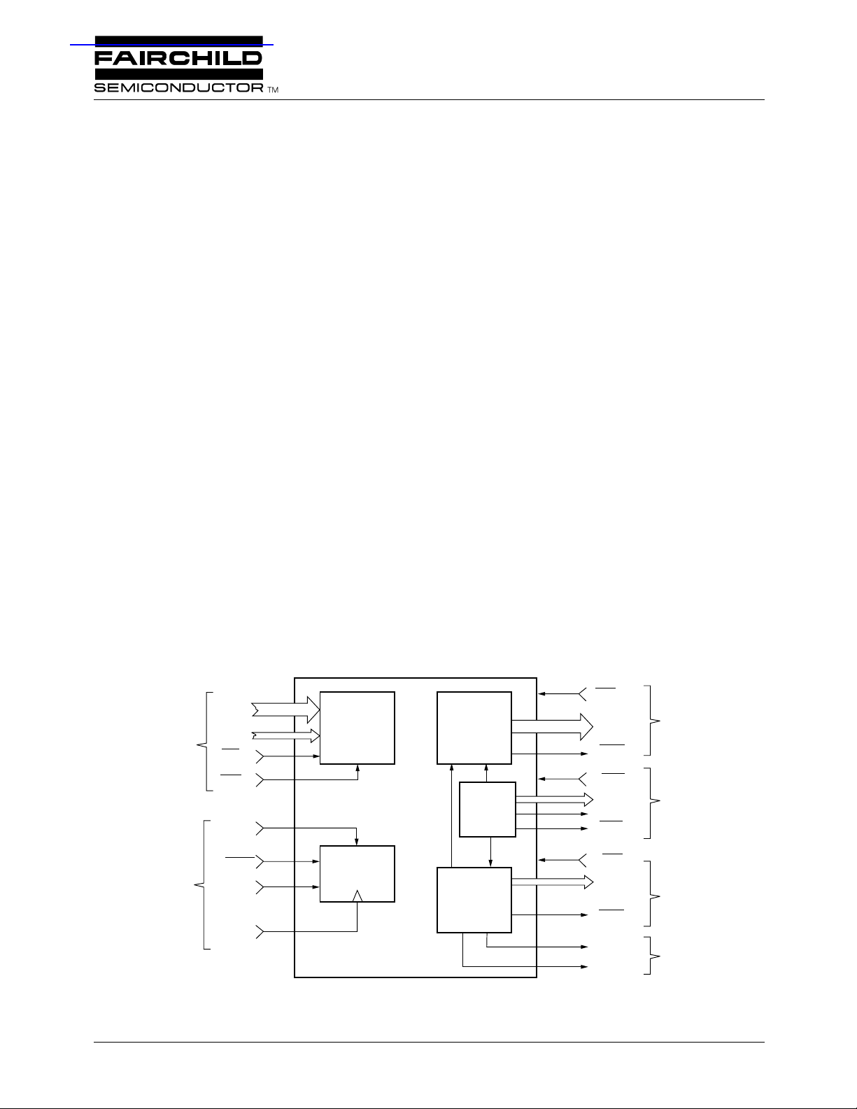
Simplified Block Diagram
IDAT
15-0
IADR
ASYNCHRONOUS
HOST INTERFACE
SYNCHRONOUS
HOST INTERFACE
6-0
ICS
IWR
SYNC
NOOP
INIT
CLK
CONTROL
PARAMETER
REGISTERS
CONTROL
SOURCE
ADDRESS
GENERATOR
WALK
COUNTER
TARGET
ADDRESS
GENERATOR
65-2302-01
OES
SADR
SVAL
OEK
KADR
ACC
TWR
OET
TADR
TVAL
END
DONE
SOURCE MEMORY
23-0
7-0
11-0
INTERFACE
CONVOLUTIONAL
TARGET
MEMORY
INTERFACE
SYNC FLAGS
CONTROL
Rev. 0.9.2
TMC2302A PRODUCT SPECIFICATION
Description
(continued)
A system based on two TMC2302As can nearest-neighbor
resample a two-dimensional 512 x 512 pixel image in 6.5
milliseconds, translating, rotating, or warping it, depending
on the user-selected transformation parameters. A complete
bilinear interpolation of the sample image can be completed
in 26 milliseconds (or 6.5ms with a TMC2246A companion
chip), while a nearest-neighbor resampling of a 3D image
128 pixels on a side takes only 53 milliseconds with three
TMC2302As. Image resampling speed is independent of
angle of rotation, degree of warp, or amount of zoom specified.
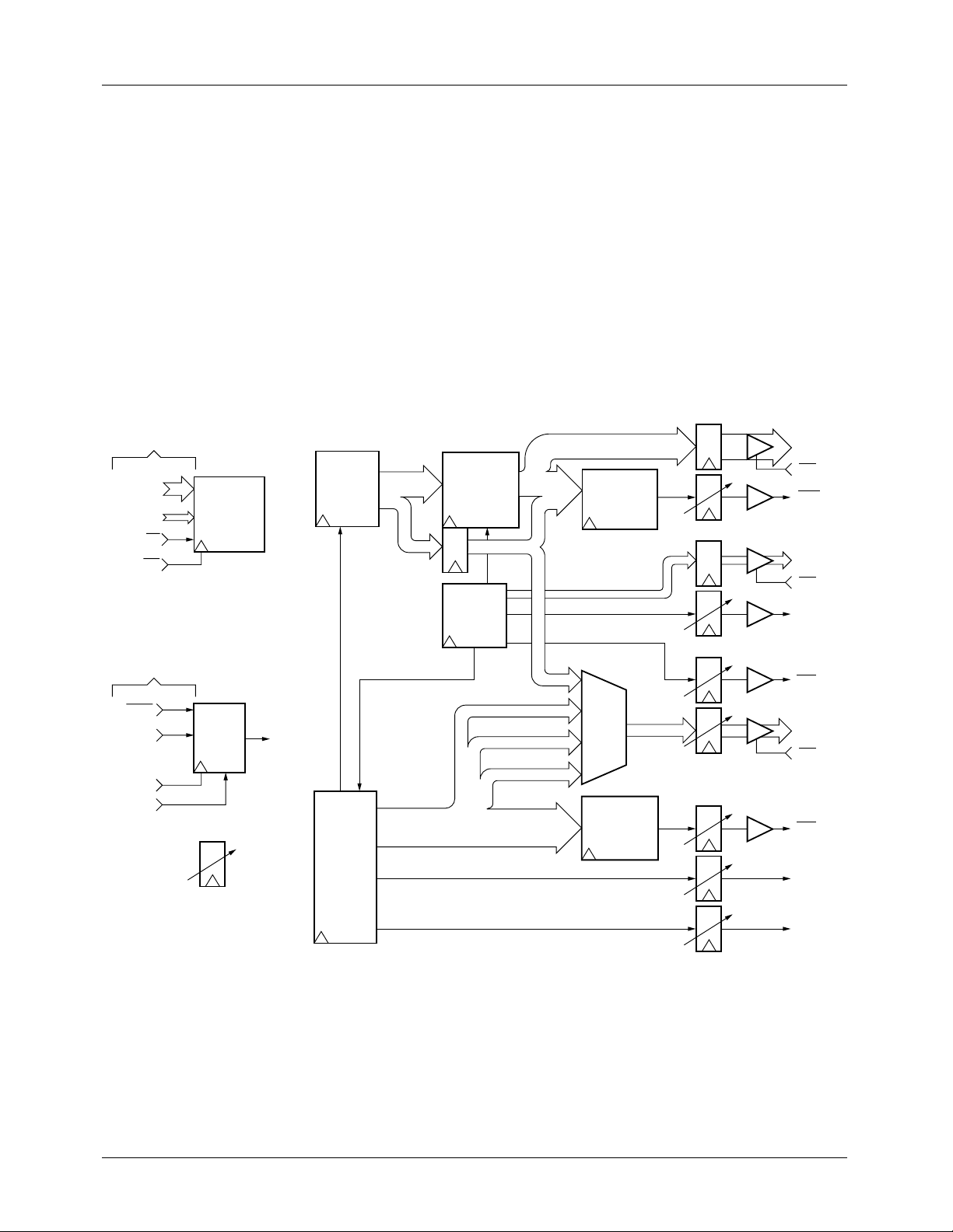
Block Diagram
ASYNCHRONOUS
HOST INTERFACE
IDAT
15-0
IADR
6-0
ICS
IWR
SYNCHRONOUS
HOST INTERFACE
CONTROL
PARAMETER
AND ADDRESS
BUFFER
SOURCE
ADDRESS
GENERATOR
48-BITS
(47-24)
(23-12)
KERNEL WALK
ACCUMULATOR
The TMC2302A can process image data fields with up to 24
bits of binary resolution (2
24
pixels) per dimension, with 0 to
16-bit subpixel resolution.
Along with the original Plastic Pin Grid Array (PPGA)
package, the TMC2302A is offered in a 120-lead Metric
Quad FlatPack (MQFP) as well. All TMC2302 electrical,
functional, and environmental specifications are improved or
remain unchanged in the TMC2302A.
SOURCE MEMORY
OFFSET
24-BITS
WALK
COUNTER
8-BITS
COMPARATOR
(7-0)
BOUNDARY
36-BITS
CONVOLUTIONAL
TARGET MEMORY
INTERFACE
INTERFACE
SADR
OES
SVAL
CONTROL
KADR
OEK
ACC
TWR
23-0
7-0
NOOP
INT
CLK
SYNC
Preliminary Information
PROGRAMMABLE
DELAY
0 TO 7 CLOCKS
CONTROL
INTERNAL
CLOCK
TARGET
ADDRESS
GENERATOR
3 X 13-BITS
X(11-0)
Y(11-0)
Z(11-0)
3-D BOUNDARY
COMPARATOR
3 x 13 BITS
TADR
OET
TVAL
END
DONE
65-2302-02
11-0
2
PRODUCT SPECIFICATION TMC2302A
Functional Description
General Information
The TMC2302A is a versatile, high-performance address
generator which can control, under user direction, filtering or
remapping of two or three-dimensional images by resampling them from one set of Cartesian coordinates (x, y, z)
into a new, transformed set (u, v, w). Most applications
utilize two identical devices for two-dimensional, or three
devices for three-dimensional, image processing. The host
CPU initializes the system by loading the input image buffer
RAM with the source image pixel data and the TMC2302As
with the image transformation and system configuration control parameters. These parameters are loaded by a separate,
asynchronous input clock. The IMS-based system then executes the entire transformation as programmed, generating a
DONE flag upon completion of the transform. The user can
program the chip to repeat the transform continuously or to
halt at the end.
The IMSs continuously compute the target bit plane (u, v) or
bit space addresses (u, v, w) in typical line-by-line, rasterscan serial sequence. For each output pixel address, they
compute the corresponding remapped source image coordinates, each of whose upper 24 bits become the source bit
plane addresses (x, y). An additional lower twelve bits are
available through the target address port in the optional
extended address mode. Source image addresses may be
generated at up to 40MHz, with the corresponding target
image addresses then appearing at up to (40/k)MHz, where
“k” is the size of the interpolation kernel implemented. In the
two-IMS system, one TMC2302A computes the horizontal
coordinates x and u while the other generates the y and v
(vertical) addresses. In a three-dimensional system, one
additional IMS would provide the z and w (depth or time)
coordinates.
T o support a wide range of image transformations, the “ro w”
or x/u device implements a 16-term polynomial of the form:
x = a + bu + cu
2
+ jv
u + kv
2
u
3
+ du
+ ev + fvu + gvu
2
2
3
+ lv
u
+ mv
3
+ nv
3
u + ov
2
+ hvu
3
2
+ iv
3
2
3
+ pv
3
u
u
2
where "a" through "p" are the user-defined image transformation parameters. The TMC2302A steps sequentially
through the pixels within a user-defined rectangle in the target image space, computing the “old” source image address
(x, y, z) corresponding to each “new” target image pixel (u,
v, w). User-programmable flags are available to indicate
when the source and target image addresses have fallen outside of a defined rectangular area, simplifying the generation
of complex images or image windows. Here, u = U-UMIN
and v = V-VMIN, where (u,v) is the target address output by
the TMC2302A.
In the three-dimensional mode, the x/u transformation equation is:
x = a + bu + ev + kw + fuv + ivw + luw + juvw
See “The Image Transformation Polynomial” section of the
Applications Discussion.
Preliminary Information
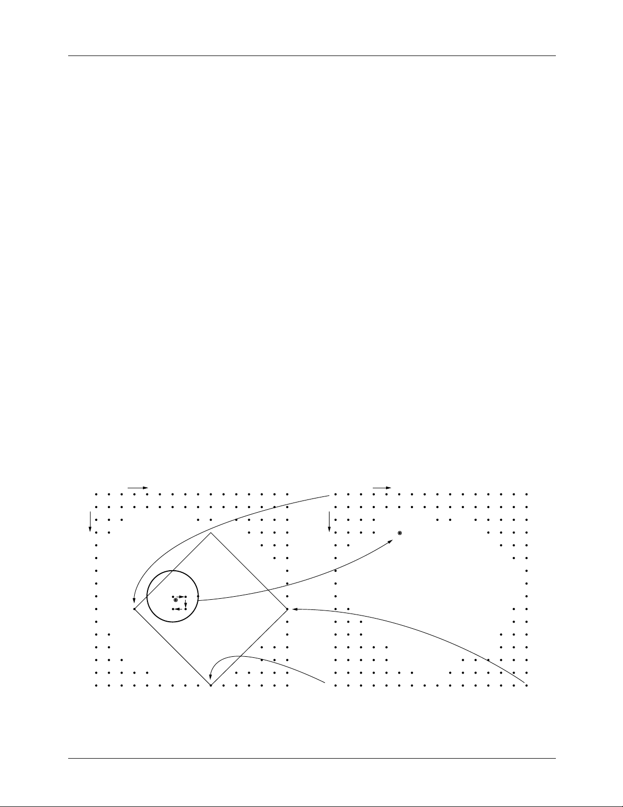
(XMIN, YMIN) ORIGINAL (SOURCE) IMAGE NEW (TARGET) IMAGE
y
x
(U0, V0)
NOTE 2
(XMAX, YMAX)
Notes:
1. Coordinate transformation U, V pixel mapped into X, Y coordinates.
2. Bilinear pixel interpolation walk. New U, V pixel intensity calculated from surrounding X, Y pixel neigborhood.
Figure 1. Image resampling geometry showing two-dimensional image rotation and expansion
(UMIN, VMIN)
NOTE 1
U
V
NEW PIXEL
(UMAX, VMAX)
65-2302-03
3
TMC2302A PRODUCT SPECIFICATION
The TMC2302A utilizes an external multiplier-accumulator
or interpolator, connected to the system clock, to calculate
the interpolated pixel value for each color. The products of
the original source image pixel values surrounding the
remapped pixel location (interpolation kernel) and the appropriate weights stored in the coefficient lookup table are
summed. The resulting new interpolated image pixel v alue is
then stored in the corresponding (u, v, w) memory location in
the target image memory buffer. Next, the target image
address is incremented by one in the “u” direction until
UMAX is reached (end of line), when u is reset to UMIN,
and the v counter is incremented to give the first pixel location in the next line. The process is repeated, proceeding
line-by-line through the image, until VMAX is reached. In
the case of three-dimensional images, the IMS system also
steps through each page in the image, incrementing in the
“w” direction with the completion of each image plane until
WMAX is reached, and the transformation is complete.
The Image Manipulation Sequencer can support any nearestneighbor, bilinear interpolation, or cubic convolution resampling. Interpolation kernels of more than one pixel require an
external interpolation coefficient lookup table and multiplier-
accumulator or multiple multiplier array. One, two, and
three-pass algorithms are supported. For each output point in
a typical two-dimensional single-pass static image filter, the
TMC2302A implements a spiralling pixel resampling algorithm, “walking” around the resampling neighborhood in
two dimensions and generating the appropriate coefficient
table addresses to sum up the interpolated pixel value in the
external pixel interpolator. At the end of each walk, the
TMC2302A will advance one pixel along the output scan
line and then execute the walk for that next pixel. When performing multiple-pass interpolation, the TMC2302A system
proceeds along only one dimension per pass, which requires
dimensionally separable, preferably orthogonal, coefficients.
A basic, two-dimensional TMC2302A-based system is
shown in Figure 2 . In this typical arrangement, two Image
Manipulation Sequencers process the image. The only other
components needed beyond the source and target image
buffer memories are a multiplier-accumulator or pixel interpolator such as the TMC2246A Image Mixer or TMC2250A
Matrix Multiplier, and the Interpolation Coefficient Lookup
Table RAM or ROM.
INITIALIZATION
DATA
CONTROL
Preliminary Information
CLOCK
Figure 2. Basic two-dimensional image convolver using TMC2302A IMS with typical 8-bit data path
IMAGE DATA IN
8
16
IDAT
15-0
IDAR
6-0
KADR
INTERPOLATION
DATA
IN
IDAT
15-0
IDAR
6-0
SADR
TMC2302A
ROW (X)
TADR
, SADR
7-0
16
ADDRESS
COEFFICIENT
BUFFER RAM
ADDRESS
8
SADR
7-0
SADR
TMC2302A
ROW (Y)
TADR
23-8
ACC
TWR
7-0
DATA
OUT
23-8
16 2 x 16
11-0
16
11-0
2 x 24
SOURCE
ADDRESS
CLOCK
DESTINATION
ADDRESS
SOURCE
IMAGE
BUFFER
RAM
8
X
ACC
X, Y, P
Y
MULTIPLIER-
ACCUMULATOR
8
WR
DESTINATION
IMAGE
BUFFER
RAM
8
IMAGE DATA OUT
65-2302-04
4
PRODUCT SPECIFICATION TMC2302A
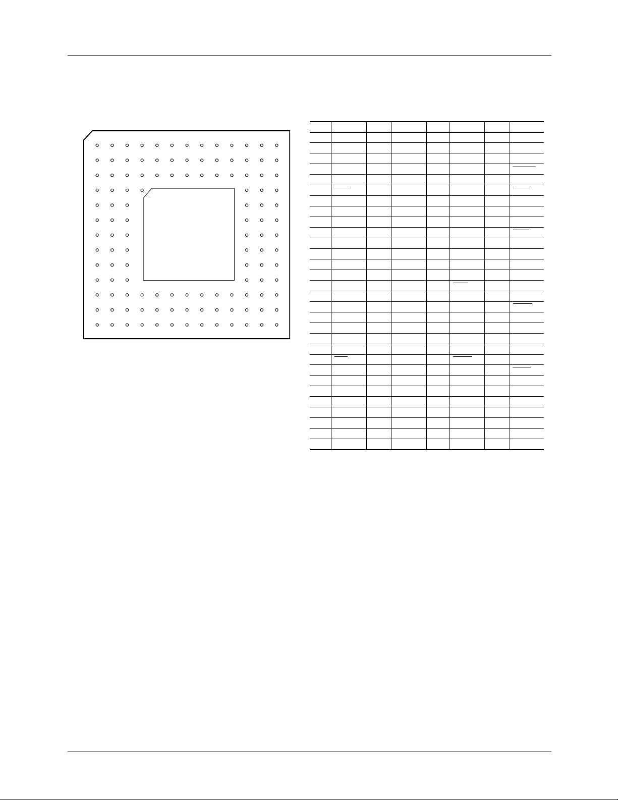
Pin Assignments
120 Pin Plastic Pin Grid Array, PPGA
12345678910111213
A
B
C
D
E
KEY
F
G
Top View
Cavity Up
H
J
K
L
M
N
65-2302-05
Pin Name Pin Name
C5
C6
C7
C8
C9
C10
C11
C12
C13
D1
D2
D3
D11
D12
D13
E1
E2
E3
E11
E12
E13
F1
F2
F3
F11
F12
F13
G1
G2
G3
SADR
SADR
IADR
IADR
IDAT
IDAT
GND
GND
IDAT
SADR
SADR
GND
V
DD
IDAT
IDAT
SADR
SADR
GND
GND
IDAT
IDAT
SADR
SADR
V
DD
V
DD
GND
IDAT
SADR
GND
V
DD
A1
A2
A3
A4
A5
A6
A7
A8
A9
A10
A11
A12
A13
B1
B2
B3
B4
B5
B6
B7
B8
B9
B10
B11
B12
B13
C1
C2
C3
C4
GND
SADR
SADR
V
DD
SADR
OES
IADR
IADR
IADR
IDAT
IDAT
IDAT
V
DD
SADR
SADR
V
DD
SADR
SADR
SADR
IADR
IADR
ICS
IDAT
IDAT
IDAT
IDAT
SADR
V
DD
V
DD
GND
16
17
21
6
3
0
15
12
9
14
15
18
20
23
4
2
13
11
8
7
13
Pin Name Pin Name
GND
G11
19
22
5
1
14
10
6
11
12
5
4
9
10
3
2
7
8
1
6
G12
G13
H1
H2
H3
H11
H12
H13
J1
J2
J3
J11
J12
J13
K1
K2
K3
K11
K12
K13
L1
L2
L3
L4
L5
L6
L7
L8
L9
V
DD
IDAT
SADR
SADR
GND
GND
V
DD
SYNC
SADR
SADR
V
DD
V
DD
CLK
IWR
SADR
SADR
GND
V
DD
INIT
GND
SVAL
V
DD
NC
V
DD
GND
KADR
V
DD
TADR
TADR
0
5
4
3
2
1
0
0
4
8
L10
L11
L12
L13
M1
M2
M3
M4
M5
M6
M7
M8
M9
M10
M11
M12
M13
N1
N2
N3
N4
N5
N6
N7
N8
N9
N10
N11
N12
N13
DONE
V
DD
GND
NOOP
ACC
OEK
KADR
KADR
KADR
OET
TADR
TADR
TADR
TADR
GND
GND
TVAL
GND
KADR
KADR
KADR
KADR
TWR
TADR
TADR
TADR
TADR
TADR
TADR
ENDD
6
4
2
0
3
6
9
7
5
3
1
1
2
5
7
10
11
Preliminary Information
5
TMC2302A PRODUCT SPECIFICATION
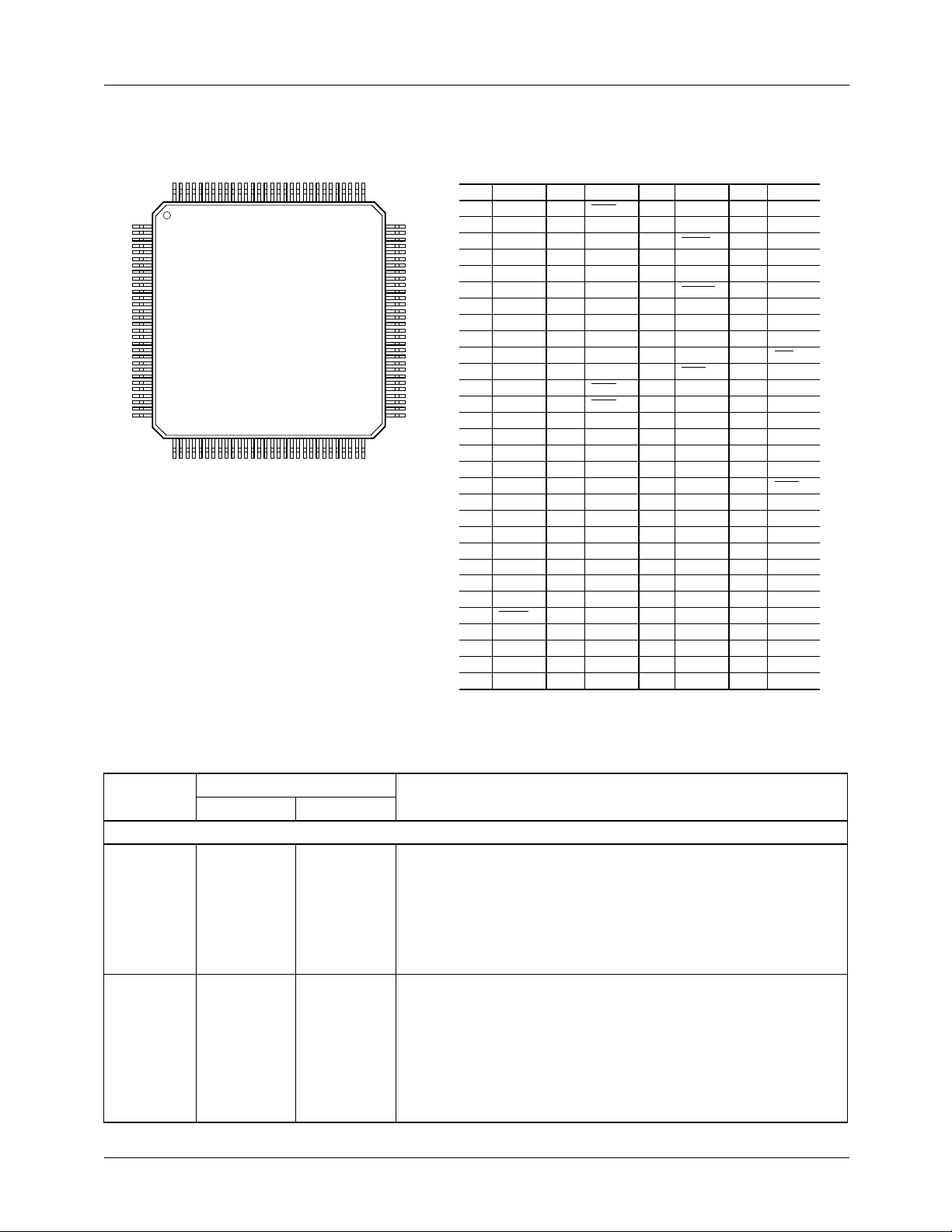
Pin Assignments
(continued)
120 Lead Metric Quad Flat Pack, MQFP
120 91
1
30
31 60
90
61
65-2302-06
Pin Name Pin Name
1
2
3
4
5
6
7
8
9
10
11
12
13
14
15
16
17
18
19
20
21
22
23
24
25
26
27
28
29
30
V
DD
SADR
SADR
GND
V
DD
SADR
SADR
GND
SADR
SADR
SADR
V
DD
SADR
SADR
GND
V
DD
SADR
SADR
SADR
GND
SADR
SADR
SADR
V
DD
SADR
SVAL
ACC
GND
V
DD
GND
31
OEK
32
33
34
35
36
37
38
39
40
41
42
43
44
45
46
47
48
49
50
51
52
53
54
55
56
57
58
59
60
KADR
V
DD
KADR
KADR
KADR
GND
KADR
KADR
KADR
KADR
OET
TWR
TADR
V
DD
TADR
TADR
TADR
TADR
TADR
TADR
TADR
TADR
TADR
TADR
TADR
DONE
GND
NC
ENDD
15
14
13
12
11
10
9
8
7
6
5
4
3
2
1
0
Pin Name Pin Name
V
61
DD
GND
62
7
63
TVAL
V
64
6
5
4
3
2
1
0
0
1
2
3
4
5
6
7
8
9
10
11
65
66
67
68
69
70
71
72
73
74
75
76
77
78
79
80
81
82
83
84
85
86
87
88
89
90
DD
GND
NOOP
INIT
V
DD
GND
CLK
IWR
GND
V
DD
SYNC
V
DD
GND
IDAT
IDAT
GND
V
DD
IDAT
IDAT
IDAT
GND
IDAT
IDAT
IDAT
V
DD
GND
V
DD
91
92
93
94
95
96
97
98
99
100
101
102
103
104
105
106
107
0
108
1
109
110
111
2
112
3
113
4
114
115
5
116
6
117
7
118
119
120
GND
IDAT
IDAT
IDAT
IDAT
IDAT
IDAT
IDAT
IDAT
ICS
IADR
IADR
IADR
IADR
IADR
IADR
IADR
OES
SADR
SADR
SADR
SADR
V
DD
SADR
SADR
SADR
SADR
GND
V
DD
GND
8
9
10
11
12
13
14
15
0
1
2
3
4
5
6
23
22
21
20
19
18
17
16
Pin Descriptions
Pin Name
Preliminary Information
Power
V
DD
GND D3, E3, G2,
6
Pin Number
C3, C2, F3,
G3, J3, L2,
L4, L7, L11,
K11, J11,
H12, G12,
F11, D11,
A13, A4, B3
H3, K3, N1,
L5, M11,
M12, L12,
K13, H11,
G11, F12,
E11, C12,
C11, C4, A1
1, 5, 12, 16,
24, 29, 33,
45, 61, 64,
68, 73, 75,
80, 88, 90,
113, 119
4, 8, 15, 20,
28, 30, 37,
58, 62, 65,
69, 72, 76,
79, 84, 89,
91, 118, 120
Pin Function DescriptionPPGA MQFP
Supply Voltage. The TMC2302A operates from a single +5V
supply. All pins must be connected.
Ground.
PRODUCT SPECIFICATION TMC2302A
Pin Descriptions
(continued)
Pin Number
Pin Name
Clocks
CLK J12 70
IWR
J13 71
Inputs
IDAT
15-0
A10, C9,
B10, A11,
B11, C10,
A12, B12,
B13, C13,
D12, D13,
E12, E13,
F13, G13
IADR
6-0
A7, C7, B7,
A8, B8, C8,
A9
Outputs
SADR
23-0
B6, C6, A5,
B5, C5, B4,
A3, A2, B2,
B1, C1, D2,
D1, E2, E1,
F2, F1, G1.
H1, H2, J1,
J2, K1, K2
KADR
7-0
N2, M3, N3,
M4, N4, M5,
N5, L6
99, 98, 97,
96, 95, 94,
93, 92, 87,
86, 85, 83,
82, 81, 78,
77
107, 106,
105, 104,
103, 102,
101
109, 110,
111, 112,
114, 115,
116, 117, 2,
3, 6, 7, 9,
10, 11, 13,
14, 17, 18,
19, 21, 22,
23, 25
32, 34, 35,
36, 38, 39,
40, 41
Pin Function DescriptionPPGA MQFP
System Clock . The pixel clock of the TMC2302A strobes all
internal registers except the control parameter preload registers.
All timing specifications except those are referenced to the rising
edge of CLK.
Input Parameter Write Clock. The internal image transformation
and configuration control parameter registers are double buffered
to simplify interfacing with system controllers. Depending on the
state of the chip selects ICS
, control words input to IDAT
the corresponding addresses presented to IADR
are strobed
6-0
15-0
and
into the outer preload registers on the rising edge of the Input
parameter Write clock IWR
. The last parameter must be loaded
twice on two consecutive rising edges of IWR.
Input Parameter Data. Configuration and transformation
parameter Input Data are presented, along with the appropriate
input register address word IADR
, to the parameter Input Data
6-0
port, and are latched into the preload registers on the next rising
edge of IWR
. Preload register updates are disabled by the chip
select control ICS. See Figure 3.
Input Parameter Address. The input parameter preload register
currently indicated by the Input parameter register Address
IADR
rising edge of IWR
is loaded with the data presented to input port IDAT on the
6-0
, as demonstrated in Figure 3.
Source Address. The 24-bit address of one dimension (X, Y, Z) of
the source image pixel value currently being resampled is output
through the Source Address port SADR
forced to the high-impedance state by the enable control OES
. This port can be
23-0
.
Coefficient Address. The integer address steps for each
dimension of the spiral interpolation walk performed by the
TMC2302A, as determined by the transform parameter KERNEL,
are generated by the internal walk counter and output at the
Coefficient Address output port KADR
to the high-impedance state by the enable control OEK
. This port can be forced
7-0
.
Preliminary Information
7
TMC2302A PRODUCT SPECIFICATION
Pin Descriptions
Pin Name
TADR
11-0
Controls
INIT K12 67
SYNC H13 74
ICS B9 100
Preliminary Information
ACC M1 27
N12, N11,
M10, L9,
N10, M9,
N9, L8, M8,
N8, N7, M7
(continued)
Pin Number
56, 55, 54,
53, 52, 51,
50, 49, 48,
47, 46, 44
Pin Function DescriptionPPGA MQFP
Target Address. The 12-bit address of one dimension (U, V, W) of
the target image pixel value just resampled is output through the
Target Address Port TADR
impedance state by the enable control OET
delayed up to seven clock cycles after the nominal sequence
shown in Table 4 by utilization of the pipeline delay parameter
PIPTAD. For systems requiring greater spatial resolution in the
source image than that offered by the SADR
Address Port can be reconfigured to output 12 additional LSBs of
the source address by placing the device into the Extended mode,
in which case the pipeline delay parameter must be set to 0 to
maintain alignment with the current source address port output.
See the Device Configuration and Control Parameters section.
Initialize. The TMC2302A control logic is cleared and initialized for
the start of a new image transformation, and the internal working
registers are updated with the contents of the current control
parameter preload registers when the registered control input INIT
is HIGH. The image transformation then commences with the first
source image pixel address nine clocks after INIT is returned low.
Run/Halt. The user can select between continuous or one-frame
operation with the registered input control SYNC. Assuming that
INIT remains LOW and NOOP
HIGH at the end of a transform the TMC2302A will begin the next
image transformation without interruption. This assumes either that
the user is not changing the parameter set, or that a new set of
parameters has already been loaded into the preload registers
midframe, prior to the beginning of the last line in the transform. If
SYNC is LOW during the last clock cycle of a transform, the device
will complete the image, having loaded the new transform
parameter set during the first clock of the final line of the transform,
and halt in the state set on the first clock cycle of the next
transform. These outputs are held until SYNC is again brought
HIGH, and operation resumes on the next clock. See Figure 5.
Input Parameter Chip Select. The input parameter preload
register write clock IWR, and thus the preloading of all
configuration and transformation parameters, is disabled on the
next clock when the registered Input parameter Chip Select input is
HIGH. When ICS returns LOW, they are enabled on the next clock.
See Figure 3
Accumulate. The external pixel interpolator or multiplier-
accumulator is initialized for a new accumulation of products by the
registered Accumulator Control output ACC. On the first cycle of
each interpolation walk, this output goes LOW for one cycle,
effectively clearing the register by loading in only the first new
resampled pixel value. When performing nearest-neighbor
resampling, this control will remain LOW throughout the entire
transform. This output can be delayed up to seven clock cycles
after the nominal sequence shown in Table 4 by the pipeline delay
parameter PIPACC. See the Device Configuration and Control
Parameters section.
.
. This port is forced into the high-
11-0
. TADR
23-0
remains HIGH, if SYNC remains
can be
11-0
alone, the Target
8
PRODUCT SPECIFICATION TMC2302A
Pin Descriptions
Pin Name
TWR
NOOP
OES A6 108
OEK M2 31
OET M6 42
Flags
SVAL L1 26
N6 43
L13 66
(continued)
Pin Number
Pin Function DescriptionPPGA MQFP
Target Memory Write Enable. On the last cycle of each
interpolation walk, the Target Write Enable goes LOW for one clock
cycle, returning HIGH for all but the last cycle of the next walk.
When performing nearest-neighbor resampling, this control will
remain LOW throughout the entire transform. This output can be
forced to the high-impedance state by the enable control OET, and
can be delayed up to seven clock cycles after the nominal
sequence shown in Table 4 by the pipe-line delay parameter
PIPTWR. See the Device Configuration and Control Parameters
section.
No Operation. Assuming that INIT remains LOW, the internal
system clock of the TMC2302A will be disabled on the next clock,
halting the current transform, when the registered control input
NOOP goes LOW. When NOOP returns HIGH, normal operation
resumes on the next clock. This control does not affect the loading
of the configuration and transformation parameter preread
registers.
Source Address Output Enable. The source address port
SADR
is LOW. When OES is HIGH, the port is in the high-impedance
state.
Coefficient Address Output Enable. The interpolation coefficient
address port KADR
enable OEK
impedance state.
Target Address Output Enable. The target address port TADR
and target write enable TWR
0
asynchronous Target Output Enable OET is LOW. When OET is
HIGH, these outputs are in the high-impedance state. This control
functions in both the normal and extended addressing modes.
Source Address Valid. When the current source image address
component output is within the working space defined by the
parameters XMIN and XMAX (or YMIN, YMAX for the column (Y/V)
device or ZMIN, ZMAX for the page (Z/W) device), the Source
Address Valid flag SVAL for that device is LOW. This flag will go
HIGH on the clock in which the corresponding component address
falls outside the defined region. In a typical system, the SVAL
outputs of all IMS devices are OR’ed together to generate a global
boundary violation flag. The user might then insert zeroes into the
pixel interpolator to ignore that portion of the image outside the
defined space, or insert a background color or image. This output
can be delayed up to seven clock cycles after the nominal
sequence shown in Table 4 by the pipeline delay parameter
PIPSVA. See the Device Configuration and Control Parameters
section.
is enabled when the asynchronous output enable OES
23-0
is enabled when the asynchro- nous output
7-0
is LOW. When OEK is HIGH, the port is in the high-
are enabled when the
11-
Preliminary Information
9
TMC2302A PRODUCT SPECIFICATION
Pin Descriptions (continued)
Pin Number
Pin Name
TVAL
ENDD N13 60
DONE L10 57 Done. On the last clock cycle of the current image transform, the
No Connects
NC L3 59 No Connect.
Preliminary Information
M13 63
D4 — Index Pin.
Pin Function DescriptionPPGA MQFP
Target Address Valid. When the current target image addresses
are within the working space defined by the parameters UMINI and
UMAXI, and VMINI and VMAXI (and WMINI and WMAXI for
systems processing three-dimensional images), the Target
Address Valid flag TVAL for that device is LOW. This flag will go
HIGH on the clock in which the current target address outputs fall
outside the defined region, which must fall inside the target area
defined by UMIN, UMAX, etc. Since each TMC2302A device is
programmed with distinct MINI/MAXI parameters and generates a
separate TVAL
dimensional target space windows for each device. TVAL can be
delayed up to seven clock cycles after the nominal sequence
shown in Table 4 by the pipeline delay parameter PIPTVA. See the
Device Configuration and Control Parameters section.
End of Dimension. During the last pixel interpolation walk of a row
(X/U device), the last row in a page (Y/V device), or the last page in
a three-dimensional transform (Z/W device), the flag ENDD goes
HIGH for the entire walk, indicating End of the transform in that
dimension. It remains LOW otherwise. This output can be delayed
up to seven clock cycles after the nominal sequence shown in
Table 4 by the pipeline delay parameter PIPEND. See the Device
Configuration and Control Parameters section.
DONE flags on all TMC2302As go HIGH for one clock cycle. On
the next clock cycle, all devices output the first addresses and
control signals for the next image transform. If SYNC is LOW, the
IMS system halts. If SYNC is HIGH, operation continues without
interruption. See “SYNC,” in the Controls section. This flag can be
delayed up to seven clock cycles after the nominal sequence
shown in Table 4 by the pipeline delay parameter PIPDON. Also
see “PFLS,” in the Device Configuration and Control Parameters
section.
flag, the user may define separate two or three-
10

PRODUCT SPECIFICATION TMC2302A
Transformation Coefficient and
Configuration and Control
Parameters
The TMC2302A is intended to act as a co-processor, requiring only that the user program the device to perform the
image transformation desired by loading in the appropriate
device configuration and transformation control parameters
discussed in this section. The user then issues an “Init”
command, allowing his system to run unattended until the
completion of the image when a “Done” flag is generated to
inform the host system.
The capabilities and flexibility of the TMC2302A Image
Manipulation Sequencer are apparent when reviewing the
following tables which define the transformation coefficient
and configuration and control parameters. These tables are
broken up into two separate groups. The first parameters discussed are the control words which select the dimension calculated, the functional configuration of each device, the
working space in which they will operate, the size of the
interpolation kernel desired, and the timing of the various
address and control signals involved in handling the pixel
data pipeline. The second parameters are the polynomial
transform coefficients used in performing image manipulation. The TMC2302A utilizes three levels of internal 48-bit
accumulators to calculate these values by forward difference
accumulation, generating no significant cumulative spatial
error for most applications. The user must be aware that all
internal parameter and coefficient registers must be set by
the user, including resetting after powerup any unused control words or coefficients.
As mentioned above, the TMC2302A also features userprogrammable image data pipeline configuration controls.
All output signals except the source and coefficient address
outputs can be individually delayed by the user up to seven
clocks after the nominal system timing illustrated in Table 4.
This allows the user to software-configure the TMC2302As
in his system to match his pixel interpolator, image buffer,
and interpolation coefficient RAM structure timing.
The user can also program the device to continue into the
next image for a set number of clock cycles after the Done
flag has appeared. First, this “flushes” the final resampled
pixel data word through the interpolation pipeline, all the
way to the target image RAM. Also, valid pixel data will
then appear on the first clock of the next transform independent of the length of the pixel pipeline, incurring no lost
clock cycles.
Device Configuration and Control
Parameters
UMIN,
VMIN,
WMIN
UMAX,
VMAX,
WMAX
Note: The parameter UMAX must exceed UMIN so as to
ensure that a minimum of 5 system clock cycles in twodimensional operation, or 15 clock cycles in three-dimensional operation, pass between the periods in which these
two target address values are generated. Thus in 2D nearest
neighbor operation UMAX must be 5 greater than UMIN. In
2D bilinear interpolation mode (4-pixel two-dimensional
kernel) the distance must be two pixels in the target image
(actually enforcing a spacing of 8 system clocks).
UMINI,
VMINI,
WMINI
UMAXI,
VMAXI,
WMAXI
The memory addresses of the target image
boundaries corresponding to the top, left side,
and front page of the new image being generated are defined in all devices of the user's
system by the parameters UMIN, VMIN, and
WMIN, respectively. At the beginning of the
transformation, the initial source image coordinate (X
coordinate set. The numeric format assumed
is 12-bit unsigned binary integer.
The memory addresses of the target image
boundaries corresponding to the bottom,
right side, and last page of the image being
generated are defined in all devices by the
parameters UMAX, VMAX, and WMAX,
respectively. These values should be greater
than the UMIN/VMIN/WMIN values defined
above. Numeric format assumed is unsigned
12-bit binary integer.
The target image addresses corresponding to
those of the top, left side, and front page of the
2 or 3 dimensional region indicated by the
valid target address flag TVAL are UMINI,
VMINI, and WMINI, respectively. Thus, to
define a valid region beginning at “m,” the
MINI parameter value is “m,” These parameters are assumed to be in 12-bit unsigned
binary integer format. Proper TVAL operation
requires UMIN < UMINI < UMAXI
< UMAX, etc.
The target image addresses one more than
those of the right side, bottom and back page
of the region indicated by the valid target
address flag TVAL are UMAXI, VMAXI, and
WMAXI, respectively. Thus, to define a valid
region ending at “n,” the MAXI parameter
value is “n+1”. These parameters are assumed
to be in 12-bit unsigned integer format.
, Y0, Z0) will be mapped to this
0
Preliminary Information
11

TMC2302A PRODUCT SPECIFICATION
XMIN,
XMAX
PFLS The user can set the number of clock cycles
PTAD,
PDON,
PEND,
PTVA,
PSVA,
PTWR,
PACC
XTND When the user sets the control bit XTND to 1,
Preliminary Information
E3D Setting this control bit to 0 indicates a
The source image boundaries are defined for
each device by the parameters XMIN and
XMAX, in the case of the row device.
The column device then contains YMIN and
YMAX, and the page device (in systems
performing three-dimensional operations)
ZMIN and ZMAX. The value of XMAX
should be greater than XMIN if the boundary
violation flag SVAL is to operate correctly.
These values are assumed to be in 32-bit
unsigned binary integer format.
that the TMC2302A continues in to the next
image following the DONE flag, allowing his
system to Flush all control and data pipeline
paths and halt after a maximum of seven
cycles. The numeric format assumed is threebit unsigned binary integer.
As mentioned above, the control signals and
target image pixel addresses generated by the
TMC2302A can be delayed up to seven clock
cycles after the nominal timing shown in
Table 4 by setting the appropriate Pipeline
delay word. The numeric format assumed for
all delay words is three-bit unsigned binary
integer.
the TMC2302A operates in an extendedresolution source address bus configuration.
Assuming that the user has his own raster scan
generator available elsewhere to manage the
flow of output pixels from the TMC2302A
system, the target address output bus TADR
is reconfigured internally into an extension of
the source address bus, as SADR
original source address bus SADR
SADR
lution in the source address space. An XTND
of 0 puts the device in the standard 24-bit
source, 12-bit target address configuration.
two-dimensional image transform is to be
performed. When the E3D is set to 1, a threedimensional image is assumed, using three
TMC2302A devices.
, providing 36 bits of spatial reso-
35-12
11-0
23-0
. The
is then
11-0
MODE In systems performing the standard two-dimen-
sional spiral interpolation walk, MODE is set
to 11, indicating single-pass operation. When
performing multiple-pass resampling, the user
must set this two-bit control word pass-by-pass
in all IMSs, to implement each pass direction.
For instance, setting MODE to 00 causes the
TMC2302A system to increment only in the
X-direction, holding the Y (and Z) addresses
constant until the end of that pixel walk. On the
next pass through the image, the user sets
MODE = 01, with the kernel increment in Y
only. In 3D, the IMS system then proceeds again
through the (U, V) target image space, walking
kernels only along the Z direction.
Mode
1,0
00 X-Pass
01 Y-Pass
10 Z-Pass
11 Two-Dimension Spiral Walk
KERNEL This parameter determines the size of the inter-
polation walk performed. To implement a
convolutional sum of K+1 pixels, the parameter
KERNEL is set to K, up to a maximum of 255.
In single-pass operation, this value must be
identical in all devices, giving a square interpolation kernel. In multiple-pass operation, however, non- square kernels may be implemented,
with different K values in each dimension. Or,
the user could utilize a banded memory architecture in two-pass mode to access an entire row or
FOV The user determines the size of each step in an
column of a kernel in one clock, completing the
entire sum in a single pass through the other
dimension of the kernel. Numeric format is 8-bit
unsigned integer.
interpolation walk, in terms of the number of
source image pixels, by setting the Field Of
Vie w control. The binary weighting of the image
transformation parameters and source address
must be taken into account when determining
this value. See Table 6 and the Applications
Discussion section. The numeric format
assumed is unsigned 16-bit integer.
Resampling Performed
DIM The user sets each TMC2302A to operate in a
specific dimension as follows:
12
DIM
1,0
00 X/U (Row) Device
01 Y/V (Column) Device
10 Z/W (Page) Device
11 No Operation
Dimension

PRODUCT SPECIFICATION TMC2302A
Table 1. Control Parameter Registers Binary Format (Row, Column or Page Device)
Addr Format Limits
Name Hex MSB LSB Dec Hex
1
UMIN 30 2
UMAX 31 2
UMINI 32 2
UMAXI 33 2
VMIN 34 2
VMAX 35 2
VMINI 36 2
VMAXI 37 2
WMIN 38 2
WMAX 39 2
WMINI 3A 2
WMAXI 3B 2
1
1
1
XMINL 3C 2
XMINM 3D 2
XMAXL 3E 2
XMAXM 3F 2
2
5
4
3
3
2
1
0
1
1
2
5
4
3
3
2
1
0
PFLS 40 22212
1
2
2
3
2
2
2
2
2
9
8
1
1
2
2
3
2
2
2
2
2
9
8
0
PTAD 40 22212
1
2
1
1
1
1
1
1
1
1
1
1
1
1
2
1
2
7
2
1
2
7
292827262
0
1
1
2
292827262
0
1
1
2
292827262
0
1
1
2
292827262
0
1
1
2
292827262
0
1
1
2
292827262
0
1
1
2
292827262
0
1
1
2
292827262
0
1
1
2
292827262
0
1
1
2
292827262
0
1
1
2
292827262
0
1
1
2
292827262
0
1
1
2
292827262
0
2
2
2
2
2
6
5
1
1
2
292827262
0
2
2
2
2
2
6
5
0
2
2
2
2
4
3
2
2
2
2
4
3
PDON 40 22212
PEND 40 2
PTVA 40 2
PSVA 41 22212
PTWR 41 22212
0
0
PACC 41 22212
XTND 41 XTND
2
2
2
2
2
2
0
0
5
5
5
5
5
5
5
5
5
5
5
5
5
21220
2
5
21220
2
2
4
3
2
2
2
2
4
2
2
2
2
2
2
2
2
2
2
2
2
2
2
3
2
2
4
3
2
2
4
3
2
2
4
3
2
2
4
3
2
2
4
3
2
2
4
3
2
2
4
3
2
2
4
3
2
2
4
3
2
2
4
3
2
2
4
3
2
2
19
2
4
2
2
1
2
18
2
3
2
19
18
2
0
1
2
2
2
2
2
2
2
2
2
2
2
2
2
2
2
2
2
2
2
2
2
2
2
2
2
2
2
2
2
2
2
204095
1
1
1
1
1
1
1
1
1
1
1
1
17
1
17
1
0
204095
0
204095
0
204095
0
204095
0
204095
0
204095
0
204095
0
204095
0
204095
0
204095
0
204095
0
200 00000000
16232
2
200 00000000
16232
2
7
0
7
0
7
0
7
0
207
0
7
0
7
0
7
0
FFF
000
FFF
000
FFF
000
FFF
000
FFF
000
FFF
000
FFF
000
FFF
000
FFF
000
FFF
000
FFF
000
FFF
000
-1 FFFFFFFF
-1 FFFFFFFF
7
0
7
0
7
0
7
0
7
0
7
0
7
0
7
0
Preliminary Information
E3D 41 E3D
DIM 41 DIM1DIM
0
MODE 41 MODE1MODE
5
4
3
2
KERNEL 42 27262
1
1
1
1
1
FOV 43 2
2
2
5
4
2
3
2
1
2
2
1
292827262
0
2
2
2
5
4
2
3
2
2
1
2
2
2
20255
1
20216-1 0FFFF
0
0
FF
00
0000
13

TMC2302A PRODUCT SPECIFICATION
Transformation Parameter Registers
The Transformation Parameter Word storage register
addresses for the X/U device are listed in Table 2, along with
the differential terms for each polynomial coefficient for
both two and three-dimensional transforms. The polynomial
terms for the other IMS device(s) are found by replacing
every “X” in the table with a Y (or Z). A TMC2302A-based
system can perform image manipulations of up to third order
The notation used to define each polynomial coefficient term
in Table 2 is easily interpreted. Each differential is of course
defined by a differential in X, followed by the corresponding
dependent U, V, or W terms. Thus,
DXUV is equivalent to d
and DXUUUV to d4X/dU3dV.
in two dimensions, and three-dimensional transforms of up
to order 1.5 (“first-and-a-half order”). Also, see “The Image
Transformation Polynomial”, in the Applications Discussion
section.
Table 2. Transformation Polynomial Coefficient Register Addresses
Parameter Coefficient Word Addresses (hex)
Name
AX
B DXU DXU 03 04 05
C DXUU 06 07 08
D DXUUU 09 0A 0B
E DXV DXV 0C 0D 0E
F DXUV DXUV 0F 10 11
G DXUUV X
H DXUUUV DXU 15 16 17
I DXVV DXVW 18 19 1A
J DXUVV DXUVW 1B 1C 1D
K DXUUVV DXW 1E 1F 20
L DXUUUVV DXUW 21 22 23
M DXVVV 24 25 26
N DXUVVV 27 28 29
O DXUUVVV 2A 2B 2C
P DXUUUVVV 2D 2E 2F
2D Term 3D Term MSW CSW LSW
0
X
0
0
00 01 02
12 13 14
2
X/dUdV
Note:
Preliminary Information
1. The X
and DXU terms must each be loaded into two different registers when performing 3D transforms. Table 2 shows the
0
binary weighting of all of the Transformation Parameter words, which are 48-bit signed fractional binary.
Table 3. Integer Binary Weighting of Transformation Parameters
Format Limits
MSB LSB Dec Hex
MSB -247246245244243242241240239238237236235234233232248-1 FFFFFFFFFFFF
CSW 2312302292282272262252242232222212202192182172
LSW 215214213212211210292827262524232221200 000000000000
Note:
1. A minus sign indicates a sign bit.
14
16

PRODUCT SPECIFICATION TMC2302A
TMC2302A
IDAT
15-0
IWR
IADR
6-0
ICS
CLK
INIT
SYNC
Figure 3. Image transformation and configuration control parameters register structure
16
PRELOAD
REGISTER
7
DE-
CODE
(a) Internal logic. Registers are enabled for the start of
each new transition or by INIT HIGH.
Figure 3 depicts the control preload register structure and
Figure 4B gives the corresponding timing relationships.
Table 4. Nominal Output Signal Timing
SADR
X
I-1,J,0
X
I-1,J,1
X
I-1,J,2
•
•
•
X
I-1,J,K
X
I,J,0
X
I,J,1
X
I,J,2
•
•
•
X
I,J,K
Note:
1. KADR
1
23-0
timing identical.
7-0
ACC TADR
0U
1U
1U
1U
0U
1U
1U
1U
11-0
L-1,M
L-1,M
L-1,M
L-1,M
L,M
L,M
L,M
L,M
EN
68
INTERNAL
REGISTER
EN
(a)
TO
REST
OF
CHIP
PIXEL
CLOCK
65-2302-07
TWR END DONE
100
100
100
010
110
110
110
011
Preliminary Information
The nominal sequence of address and control signals of a
two-dimensional, single-pass-programmed TMC2302A
system, with all PIPE parameters set to 0, is shown in
Table 4. Here, the values of the last two new target image
pixels U
L-l,M
and U
are being calculated, and the begin-
L,M
ning and end of the interpolation walks of length K which
sample source image pixels in the neighborhod of locations
(X
, X
I-1,J
image address (SADR
) can be seen. Utilizing the arrival of the source
I,J
) as a reference point, the other
31-0
signals shown can be delayed up to seven clock cycles from
the nominal timing shown here, allowing the user to configure these outputs to match the timing latencies of his pixel
data path structure. Considerable speed and timing variations
in image buffer memory, data register, and pixel interpolator
structure can thus be accomodated, with minimal corresponding support hardware. Also see “PFLS,” in the Device
Configuration and Control Parameters section.
15

TMC2302A PRODUCT SPECIFICATION
Equivalent Circuits and Threshold Levels
V
DD
n SUBSTRATE
p
p+
n
p WELL
GND
n SUBSTRATE
CONTROL
INPUT
p+
1k½
D1
p WELL
n+
D2
GND
V
DD
p
65-2302-08
Figure 5. Equivalent Input Circuit Figure 6. Equivalent Output Circuit
t
OES, OEK,
OET
Three-State
Outputs
t
DIS
0.5V
0.5V
High Impedance
ENA
2.0V
0.8V
65-2302-10
D1
n+
D2
65-2302-09
Figure 7. Threshold Levels for Three-State Measurements
Absolute Maximum Ratings
(beyond which the device may be damaged)
Parameter Min. Max. Units
Supply Voltage -0.5 + 7.0 V
Input Voltage -0.5 VDD + 0.5 V
Output applied voltage -0.5 VDD + 0.5 V
Short-circuit duration (single output in HIGH state to ground) 1 second
Preliminary Information
Operating, case temperature -60 130° C
Junction temperature 175° C
Lead, soldering temperature (10 seconds) 300°
Storage temperature -65 +150° C
Notes:
1. Absolute maximum ratings are limiting values applied individually while all other parameters are within specified operating
conditions. Functional operation under any of these conditions is NOT implied.
1
16

PRODUCT SPECIFICATION TMC2302A
Operating Conditions
-1
Parameter Test Conditions
V
V
V
l
OL
I
OH
t
CY
t
PWL
t
PWH
t
S
t
H
T
Supply Voltage 4.75 5.0 5.25 4.75 5.0 5.5 V
DD
Input Voltage, Logic LOW 0.8 0.8 V
IL
Input Voltage, Logic HIGH 2.0 2.0 V
IH
Output Current, Logic LOW 8.0 8.0 mA
Output Current, Logic HIGH -4.0 -4.0 mA
Cycle Time VDD = Min 33 25 ns
Clock Pulse Width, LOW VDD = Min 15 12.5 ns
Clock Pulse Width, HIGH VDD = Min 15 10 ns
Input Setup Time 10 8 ns
Input Hold Time 2 2 ns
Ambient Temperature, Still Air 0 70 0 70 °C
A
UnitsMin. Nom. Max. Min. Nom. Max.
Preliminary Information
Electrical Characteristics
1
Parameter Test Conditions Min. Max. Units
I
DDQ
I
DDU
Supply Current Quiescent VDD = Max, VIN = 0V 10 mA
Supply Current, Unloaded VDD = Max, f = 20MHz,
70 mA
OES = OEK = OET = 5V
I
IL
I
IH
V
V
I
OZL
OL
OH
Input Current, Logic LOW VDD = Max, VIN = 0V -10 mA
Input Current, Logic HIGH VDD = Max, VIN = V
DD
10 mA
Output Voltage, Logic LOW VDD = Min, IOL = Max 0.4 V
Output Voltage, Logic HIGH VDD = Min, IOH = Max 2.4 V
High-Z Output Leakage Current,
VDD = Max, VIN = 0V -40 mA
Output LOW
I
OZH
Hi-Z Output Leakage Current, Output
VDD = Max, VIN = V
DD
40 mA
HIGH
I
OS
Short-Circuit Output Current VDD = Max, Output HIGH,
-20 -70 mA
one pin to ground, one second
duration max.
C
I
C
O
Note:
1. Actual test conditions may vary from those shown, but guarantee operation as specified.
Input Capacitance TA = 25°C, f = 1MHz 10 pF
Output Capacitance TA = 25°C, f = 1MHz 10 pF
17

TMC2302A PRODUCT SPECIFICATION
Switching Characteristics
-1
Parameter
t
DO
t
HO
t
ENA
t
DIS
Note:
1. All transitions are measured at a 1.5V level except for t
Output Delay VDD = Min, C
Output Hold Time VDD = Max, C
Three-State Output Enable Delay
Three-State Output Disable Delay
1
1
Test Conditions Min. Max. Min. Max. Units
= 25pF 15 12 ns
LOAD
= 25pF 4 4 ns
LOAD
VDD = Min, C
VDD = Min, C
and T
DIS
EMA
= 25pF 12 12 ns
LOAD
= 25pF 15 15 ns
LOAD
.
Timing Diagrams
t
CY
PWH
t
D
t
PWL
t
H
t
HO
VALID
VALID
t
CLK
t
S
1
INPUTS
OUTPUTS
Notes:
1. Except OES, OET, and OEK.
2. Assumes OES, OET, and OEK = LOW. All pipeline latency
parameters set to 0.
2
Figure 4a. Timing Diagram, Figure 4b. Timing Diagram, Preload Parameters
Pixel Clock, Control, and Outputs
Applications Discussion
The Image Transformation Polynomial
Preliminary Information
On any given clock cycle, when performing a two-dimensional geometric transformation the addresses output by the
row (X/U) TMC2302A are generated by forward difference
accumulation according to the following third-order polynomial:
x(u,v) = a + bu + cu2 +du3 + ev + fvu + gvu2 + hvu
+ iv2 + jv2 u + kv2 u2 + Iv2 u3 + mv3 + nv3u + ov3u
+ pv3u3 + FOV • CAX(ca)
3
2
65-2302-11
t
S
IWR
IDAT
IADR
ICS
Value "DAT 1" is loaded into address "ADR 1" on the second
rising edge of IWR, since ICS = 0, having been acquired by the
input register on the first edge.
DAT 1
ADR 1
t
H
t
PWL
65-2302-12
The polynomial utilized for three-dimensional transforms is:
x(u,v,w) = a + bu + ev + kw + fuv + ivw + luw + juvw
+ FOV • CAX (ca)
where 0 £ u £ UMAX-UMIN, 0 £ v £ VMAX-VMIN,
0 £ w £ WMAX-WMIN, and the polynomials for the column
or page devices are obtained by replacing the x by a y or z, as
appropriate.
18

PRODUCT SPECIFICATION TMC2302A
FOV is the 16-bit field-of-view parameter, normally set so
that the spiral walk proceeds in single-pixel steps. FOV can
be increased to expand the step size and thus the spiral walk,
subsampling the image. See Table 1 and Table 6. Also,
CAX(ca) is the current value of the coefficient address. See
the Interpolation Coefficient Lookup Table Addressing. If
the spiral walk isn’t used, CAX = 0 and FOV is ignored.
We can reform the two-dimensional polynomial as:
x(u,v) = (a + ev + iv2 + mv3) + (b + fv + jv2 + nv3)u
+ (c + gv + kv2 + ov3)u2 + (d + hv + Iv2 + pv3)u3,
and retain the simpler three-dimensional form:
x(u, v, w) = a + bu + ev + kw + fuv + ivw + luw + juvw
and define each of the polynomial coefficients in arithmetic
terms as shown in Table 5.
Table 5. Transformation Polynomial Coefficients
Parameter
Two-Dimensional Three-Dimensional
Name Term Coefficient Term Coefficient
AX
B DXU b + c + d DXU b
C DXUU 2c + 6d — 0
D DXUUU 6d — 0
E DXV e + i + m DXV e
F DXUV f + g + h + j + k + I + n + o + p DXUV f
G DXUUV 2(g + k + o) + 6(h + I +p) X
H DXUUUV 6(h + I + p) DXU b
I DXVV 2i + 6m DXVW i
J DXUVV 2(j + k + I) + 6(n + o + p) DXUVW j
K DXUUVV 4k + 12I + 12o + 36p DXW k
L DXUUUVV 12I + 36p DXUW I
M DXVVV 6m — 0
N DXUVVV 6(n + o + p) — 0
O DXUUVVV 12o + 36p — 0
P DXUUUVVV 36p — 0
0
aX
0
0
a
a
Preliminary Information
Understanding the Polynomial
Coefficients
An Overview
As the formulae indicate, the source address is a polynomial
function of the two (or three) dimensions of the target
address. Each of the 16 terms of the equation is of the form:
mnp++
d
------------------------------- -
du
and may be treated approximately as a mixed partial
difference of order m, n, and p.
x
mdvndwp
The simplest term, X0, is a zeroeth (non-) function of the
target addresses; it specifies the source address point corresponding to the upper left point in the target space. X0
generates image translation or “pan.”
The next-simplest terms, dX/dU and dY/dV, govern the relative scales of the source and target images, i.e., how large a
step in source space corresponds to a unit step in the corresponding direction in the target space. As long as the crossterms, dX/dV and dY/dU, are zero, this is a straight scale
(“zoom”) operation, without rotation or shear.
19

TMC2302A PRODUCT SPECIFICATION
The first-order cross terms, dX/dV and dY/dU, generate
source space displacements perpendicular to unit displacements in the target space, thereby causing shearing of the
image. In conjunction with the parallel source terms
described above, they govern rotation, shear, and scaling of
the image.
Although the actions of the higher-order terms become progressively difficult to describe, all terms behave essentially
as partial differences of various orders, and a little thought
and common sense will generally lead the user to the proper
conclusions. For example, the term dXUU (using the notation of T able 2) is a horizontal scale factor which increases as
one progresses across each row, causing a quadratic horizontal warp. In fact, all terms of the form d
dny/dvn cause only stretching of the image, never rotation.
m
x/dum or
Interpolation Coefficient Lookup Table
Addressing
The external coefficient lookup table RAM stores the interpolation coefficient values used to calculate the value of the
new pixel. These values are selected by the user, allowing
maximum filtering flexibility. In simple filtering applications, the source and target pixel addresses map one-to-one,
and only one interpolation coefficient set is required. These
integer addresses are generated for each dimension by the
internal walk counters of each TMC2302A.
However, applications performing a coordinate transformation will almost always generate non-integer source pixel
addresses; that is, the U (or V) locations will not map to the
X (or Y) addresses exactly, and a fractional source address
components are generated. The user must then expand the
interpolation coefficient lookup table to include spatiallycorrected values, as detemnined by the subpixel resolution of
the system.
The TMC2301 Image Resampling Sequencer allows the user
to trade subpixel resolution against interpolation step size by
obtaining the interpolation coefficient addresses directly
Preliminary Information
from the fractional part of the source address. The
TMC2302A gives the user 16 different interpolation bit
weighting positions. The complete Interpolation Coefficient
Address for that dimension then consists of both the 8-bit
interpolation walk address KADR
source address binary point by the parameter FOV, and the
fractional portion of the source pixel address SADR
to the desired subpixel resolution. See Table 6.
, weighted to match the
7-0
23-0
Internal and External Data Formats
The source address value output by the TMC2302A is a
24-bit two's complement number, with binary point assignable by the user anywhere in the 16 lower bits. The Extended
mode appends 12 additional fractional bits for greater output
precision. All internal computations include these 24 plus 12
bits, plus an additional 12 lower bits, for 48-bit precision.
See T able 6.
Intemally, each TMC2302A's source address (X, Y,or Z)
generator computes a 48-bit address through a mode-specific
accumulation of the sixteen 48-bit user-specified resampling
parameters. The 24 most significant bits of the final accumulation emerge via the source address port whereas the
"extend" mode makes the 12 next most-significant bits available at the target address port. The 12 least significant bits
are truncated internally.
Source Address Bit Weighting and Setting the
Binary Point
When performing nearest-neighbor resampling, the user may
arbitrarily trade source image size against subpixel resolution merely by adhering to a single binary point position for
all resampling parameters. For example, if the binary point
follows the 16 most significant bits in each resampling
parameter, then it will appear following the source
address’16 most significant bits, leaving 8 (20 in extended
mode) bits of subpixel resolution on SADRn.
Since the TMC2302A has no internal limiter, the user should
select the source address weighting appropriately. Moving
the source address connections to the right and reducing the
resampling parameters accordingly, reduces the chance of
arithmetic overflow while increasing arithmetic round-error.
In any filtering or resampling operation performing an interpolation walk, the user should set the Field or View (FOV)
parameter according to the desired binary point position
determined above, as follows. To provide 224 integral pixel
positions per dimension, with no subpixel resolution, set
FOV = 001 (hex). For 223 positions with 1-bit (0,5)
subpixel resolution, FOV = 0010 (hex). Similarly, for 2
positions and 15-bit subpixel resolution. FOV = 8000 (hex).
As shown in Table 6, using the parameter FOV the user
effectively “shifts” the bit weight of the coefficient address
,
word KADR
source address binary point. In each case, the EXTEND
mode provides 12 additional bits of subpixel resolution but
eliminates the separate target or raster address, which must
then be generated elsewhere in the user's system.
to match the established location of his
7-0
9
20

PRODUCT SPECIFICATION TMC2302A
Table 6. Relative Bit Weighting – Source Address
Weight W ord 247246… 240239 … 232231 … 225224223… 216215… 212… 2827… 2
Transform
Parameters
Internal Source
Address Generator
Source Address
Output SADR
Extended Mode Only
TADR
11-0
KADR
7-0
FOV = 0001 27… 212
FOV = 0002 … 27 2
•
•
•
FOV = 8000 27… 212
Note:
1. A minus sign indicates a sign bit.
23-0
-47 46 … 40 39 … 32 31 … 25 24 23 … 16 7 … 0
-47 46 … 40 39 … 32 31 … 25 24 23 … 16 7 … 0
-23 22 … 16 15 … 8
11 … 4 3 … 0
0
6
0
… 2
0
0
Preliminary Information
Utilization of the Image Boundary
Flags SVAL and TVAL
As mentioned above, the TMC2302A provides tw o programmable valid address, or boundary flags. The source valid flag
SVAL is asserted when the current source image address
output for that device's source image dimension is within the
space defined by the configuration parameters XMIN and
XMAX, or YMIN and YMAX, or ZMIN and ZMAX, as
appropriate. Also, the target valid flag TVAL is available to
indicate when the current target image address values fall
within the space defined by the configuration parameters
UMINI, UMAXI, VMINI, VMAXI, and also WMINI and
WMAXI in three-dimensional systems. Note that all of these
parameters are each programmed into each individual
TMC2302A. Thus, the user could define two (or three) different working spaces, one indicated by each IMS device.
Figure 8 may help clarify the relationships among (X
Y0, Z0), (UMIN, VMIN, WMIN), and (UMAX, VMAX,
WMAX), for the two-dimensional case. With positive first
derivati ves, (X0, Y0) and (UMIN, VMIN) represent the upper
left corners of the original image and the new destination
field, respectively. The lower right corner of the new transformed image is located at (UMAX, VMAX); the location of
the corresponding corner of the original image depends on
the values of the derivatives.
Not to be confused with (X0, Y0), the points (XMIN, YMIN)
and (XMAX, YMAX) define the “usable” rectangular portion of the original image which is indicated by the valid
address flag SVAL; points (X, Y) lying outside this region
are ignored in most resampling and filtering applications.
,
0
Specifically, the point (X
TMC2302A system begins the image resampling sequence.
Every step beyond that point in the source image space is
defined by the address generators implementing the image
transformation polynomials.
The valid source address flag feature permits one to construct a mosaic of several abutting subimages in the (X, Y)
plane, without danger of edge effect interference between
adjacent subimages. Note in the figure that the upper right
corner of the resampled source image lies outside the admissible region; in practice, the values fetched at these locations
will not be included in the convolutional sums. One might,
for instance, program these boundary values to alert the
system that an edge is being approached and to modify the
interpolation coefficients appropriately, or simply to ignore
pixel values outside the defined space.
AL however is utilized somewhat differently. Work-
The TV
ing in unison with the target address working space defined
by UMIN/UMAX, etc. the target address valid flag could be
programmed to delineate image areas other than the immediate working space, and the flag of each TMC2302A to indicate the unique regions anywhere within the target image.
With this flexibility, the user can generate windows, “picture-in-picture” composite multiple images, or simply switch
to a background image or border color. To make TVAL function properly, the used must set UMIN < UMINI < UMAXI
< UMAX; likewise for V and, if used, W.
, Y0) is the location from which the
0
21

TMC2302A PRODUCT SPECIFICATION
X
Y
SVAL = 1
(XMIN, YMIN)
(X0, Y0)
SVAL = 0
(XMAX, YMAX)
SOURCE IMAGE SPACE TARGET IMAGE SPACE
Figure 8. Pixel maps demonstrating source and destination image boundaries, violation flags,
and image clipping (note shaded areas)
Real-Time Bilinear Interpolation
Using the TMC2302A or TMC2301
Image transformations and translations in bit mapped
systems are done by taking an original (source) image,
performing coordinate remapping and interpolation, then
restoring the image into a new (destination) image space.
The coordinates are remapped according to a transformation
U
V
TVAL = 1
(UMIN, VMIN)
(UMIN, VMIN)
(UMAX, VMAX)
TVAL = 0
(UMAX, VMAX)
65-2302-13
polynomial. The polynomial, evaluated at destination pixel
addresses, maps the transformed pixel addresses (U, V) to
pixel addresses in the original image addresses (U,V) to
pixel addresses in the original image (X, Y), i.e., (X, Y) is a
polynomial function of (U, V).
ORIGINAL (SOURCE) IMAGE NEW (TARGET) IMAGE
NOTE 1
(UMIN,VMIN)
U
V
(UMIN,VMAX)
NEW PIXEL
(U,V)
(UMAX,VMAX)
(0,0)
y
Preliminary Information
65-2302-14
x
(X0,Y0)
INTER-
POLATOR
NOTE 2
Notes:
1. Coordinate transformation: Each pixel in (U, V) space is mapped to a location in (X,Y) space.
2. Interpolation: Unless the pixel in (U, V) space coincides with one in (X, Y) space, its amplitude must be estimated as a
weighted average of those of the surrounding pixels in (X, Y) space. If the interpolation is done serially, throughput suffers in
proportion to the size of the interpolation kernel. However, the interpolation can also be performed in parallel to preserve
throughput, as discussed here.
22

PRODUCT SPECIFICATION TMC2302A
The TMC2302A Image Manipulation
Sequencer
The TMC2302A is a controller/address generator, around
which an image filtering and resampling system can be built.
Under limited supervision from an external controller, the
TMC2302A will generate the sequence of memory read and
write addresses to transform, resample, and/or filter an
image. In all cases, it fetches data from one image buffer,
governs its convolution with a user-specified kernel of
coefficients, and directs the results to another image memory
space. With 24-bit source address buses the device can
operate from a source frame size of, for example,
64K X 64K pixels with spatial resolution of 1/256th pixel. A
simplified block diagram of the TMC2302A is shown in
IDAT
ASYNCHRONOUS
HOST INTERFACE
IADR
ICS
15-0
6-0
CONTROL
PARAMETER
REGISTERS
Figure 9. Although the 24 source addresses bits of each
TMC2302A can be designed arbitrarily with the source
image address bus, assume for the current discussion that
bits SADR (19:8) will correspond to the source image
address and that SADR (7:4) therefore denote subpixel postponing to 1/16 pixel resolution.
The basic 2-D system, shown in Figure 10, consists of data
source and destination memories, coefficient lookup table,
multplier-accumulator, TMC2302A parameters to define the
transform and starts the operation. It may also control the
loading of the source image into RAM and provide the
screen refresh, if needed.
OES
SOURCE
ADDRESS
GENERATOR
SADR
SVAL
SOURCE MEMORY
23-0
INTERFACE
Preliminary Information
SYNCHRONOUS
HOST INTERFACE
IWR
NOOP
CLK
SYNC
INIT
WALK
COUNTER
CONTROL
TARGET
ADDRESS
GENERATOR
Figure 9. TMC2302A Block Diagram
OEK
KADR
ACC
TWR
OET
TADR
TVAL
END
DONE
CONVOLUTIONAL
7-0
11-0
INTERFACE
CONTROL
TARGET
MEMORY
SYNC FLAGS
65-2302-15
23

TMC2302A PRODUCT SPECIFICATION
DATA IN
8
CONTROL
DATA
CLOCK
SOURCE
ADDRESS
CLK
19-8
12
DESTINATION
ADDRESS
24
8
24
12
2302A ROW
(X)
SADR
19-8
TADR
11-0
4
ADDRESS
COEFF.
BUFFER
RAM
1024 x 8
6
ADDRESS
SADR
7-4
KADR
1-0
2302A
COLUMN (Y)
TADR
11-0
12
SADR
Figure 10. Basic 2-D Image Transformation Systems
SOURCE
IMAGE
BUFFER
A
RAM
8
X
X,Y,P
8 x 8
Y
MAC
D
OUT
8
DESTINATION
IMAGE
BUFFER
A
RAM
8
DATA OUT
HERE
4 X 4K WORDS
IMAGE SIZE
ONE SET
PER COLOR
COMPONENT
(Not recommended
for composite video)
ONE SET
PER COLOR
COMPONENT
ONE SET
PER COLOR
COMPONENT
65-2302-16
Inexact T ransformations
In many cases, evaluation of the transformation polynomial
results in a non-integer result (non-integer address in the X,
Y image space). In such cases, the mapping from original
image to transformed image will be inexact. When this
occurs, the user has the option of accepting the pixel “near-
Preliminary Information
est” to the address generated, or performing interpolation,
a weighted average of nearby pixel values. Using the pixel
nearest the address generated is the fastest method since one
transformed pixel can be generated on every cycle.
The resulting image will include jagged biasing artifacts,
however. Performing several transformations on the same
image will further degrade the resulting image.
One Cycle Bilinear Interpolation
A better image can be obtained by finding the four pixels
nearest the address generated and performing a weighted
averaging to determine the new pix el v alue. This is kno wn as
bilinear interpolation. The TMC2302A eases the control
logic required for such a function by performing a “walk”
around the four closest pixels in the source image space.
Essentially, the TMC2302A generates the addresses of the
four walk cycles, and the current source pixel is multiplied
by a weighting factor and accumulated by the external multi-
plier accumulator. At the end of the walk, the accumulated
result from the four nearest pixels is written into the destination image RAM and the TMC2302A proceeds to the next
group. The obvious disadvantage to using bilinear interpolation is that one new destination pixel is generated only on
every fourth cycle, reducing the output bandwidth by a factor
of four.
One method of “real-time” bilinear interpolation consists of
using four memories, each containing the entire source
image. The storage arrangement of the pixels within each
bank is staggered so that a single address fed to the memories
will result in the access of the proper four pixel group.
The TMC2302A is programmed to generate the nearest
neighbor address and the four nearest pixels are accessed
simultaneously and input to the four independent multipliers
of a TMC2246 quad multiplier chip. The four pixels are multiplied by their associated weighting factors and added to
determine the destination pixel sum. The major drawback of
this method is the prohibitive cost for additional memory
required to store four copies of the entire source image.
For large images, the memory cost and additional board
space makes this method unattractive.
24

PRODUCT SPECIFICATION TMC2302A
A more efficient method is to divide the original source
image into a “four-color checker board” and to store it into
four separate pixel memory banks, each containing 14th
of the source image. Since the image is separated into
four memories rather than duplicated, no additional image
memory is required. The goal is to separate the image so that
any square of four adjacent pixel locations can be accesssed
simultaneously. Thus, the user must organize the memory
such that the four pixels of any cluster will reside in separate
memory banks. With this method, only one set of address
generators (TMC2302As) is necessary, and only a slight
address modification is necessary to guarantee that the
correct group of pixels is accessed and output to the multipliers. Since all pixels are accessed simultaneously, no “walk”
is performed, and the TMC2302A system is able to generate
one destination pixel on each clock cycle. For example, a
1024 x 768 image can be generated every 20ms for a frame
refresh rate of 50Hz. This method which will be described
below.
A
0,0
(0,0)
B
0,0
(1,0)
A
1,0
(2,0)
B
1,0
(3,0)
Using Banded Pixel Memory
The TMC2302A should be programmed to do “nearestneighbor” transformations (Kernel, K = 0 and the X0 and Y0
start boundaries programmed without 1/2-LSB truncation
debiasing to force address truncation when evaluating the
transformation polynomial for the nearest-pixel address).
The biased X0 and Y0 guarantee that when the exact pixel
address falls within the region of four pixels, the upper leftmost pixel will always be selected as “nearest-neighbor.”
The key to performing real-time bilinear interpolation is to
arrange the pixels in memory so that the four pixels of every
grouping will be stored in separate memories. The four nearest pixels will form a square. Figure 11 shows a sample
512 x 512 pixel image and the arrangement into four separate memory banks designated A, B, C, and D. It can be seen
from the figure that any (square) grouping of four pixels will
have one pixel located in each bank. Thus, one memory
sector will hold even row-even column pixels, another,
even-row-add column pixels, etc.
A
2,0
(4,0)
B
2,0
(5,0)
A
3,0…A255,0
(6,0)…(510, 0)
B
255.0
(511, 0)
Preliminary Information
C
0,0
(0,1)
A
0,1
(0,2)
C
0,1
(0,3)
A
0,2
(0,4)
C
0,2
(0,5)
D
0,0
(1,1)
B
0,1
(1,1)
D
0,1
(1,3)
B
0,2
(1,4)
D
0,2
(1,5)
C
1,0
(2,1)
A
1,1
(2,1)
C
1,1
(2,3)
A
1,2
(2,4)
C
1,2
(2,5)
D
1,0
(3,1)
B
1,1
(3,2)
D
1,1
(3,3)
B
l,2
(3,4)
D
1,2
(3,5)
C
2,0
(4,1)
A
2,1
(4,2)
C
2,1
(4,3)
A
2,2
(4,4)
C
2,2
(4,5)
D
2,0
(5,1)
B
2,1
(5,2)
D
2,1
(5,3)
B
2,2
(5,4)
D
2,2
(5,5)
C
3,0…C255,0
(6,1)…(510,1)
A
3,1…A255,1
(6,2)…(510,2)
C
3,1…C255,1
(6,3)…(510,3)
A
3,2…A255,2
(6,4)…(510,4)
C
3,2…C255,2
(6,5)…(510,5)
D
255,0
(511,1)
B
255,1
(511,2)
D
255,1
(511,3)
B
255,2
(511,4)
D
255,2
(511,5)
……………… … …
A
0,255
(0,510)
C
0,255
(0,511)
Subscripts i, j for A, B, C, and D denote relative addresses in
memory respectively.
B
0,255
(1,510)
D
0,255
(1,511)
A
1,255
(2,510)
C
1,255
(2,511)
B
1,255
(3,510)
D
1,255
(3,511)
Figure 11. Source Image Pixel Arrangement
A
2,255
(4,510)
C
2,255
(4,511)
B
2,255
(5,510)
D
2,255
(5,511)
The pixels of the original image should be stored in the
source RAM banks as shown in Figure 12. The original
A
3,255…A255,255
(6,510)…(510,510)
C
3,255…C255,255
(6,511)…(510,511)
B
255,255
(511,510)
D
255,255
(511,511)
source image can be loaded by decoding the TMC2302A
The ordered pairs (a, b) denote the physical (X,Y) pixel
locations and the TMC2302A SAPR(X) and SADR(Y)
address outputs.
least significant address bits (SADRX(8). SADRY(8) to
determine the memory bank for the pixel while the
most-significant address bits (SADRX(19:9), SADRY (19:9))
are used as common address lines to all four memory banks.
25

TMC2302A PRODUCT SPECIFICATION
TMC2302A Ad-
Bank A Bank B Bank C Bank D
dress
XA
,
m
00 A
01 A
02 A
0 255 A
10 A
11 A
12 A
255 254 A
255 255 A
YA
m
XA0YA0 = 00 XA0YA0 = 10 XA0YA0 = 01 XA0YA0 = 11
0,0
0,1
0,2
0,255
1,0
1,1
1,2
255,254
255,254
B
B
In the following discussion, the TMC2302A address outputs
SADRX and SADRY will be designated as:
Horizontal Source
XA
Least-Significant Horizontal Source X-Address
0
Bit SADRX (8)
XAm Upper Horizontal Source Address Bits SADRX
(19:9)
B
0,0
B
0,1
B
0,2
B
0,255
B
1,0
B
1,1
B
1,2
255,254
255,254
C
C
C
C
0,255
C
C
C
C
255,254
C
255,254
0,0
0,1
0,2
1,0
1,1
1,2
D
D
D
D
0,255
D
D
D
D
255,254
D
255,254
0,0
0,1
0,2
l,0
1,1
1,2
B A B A B A B
*-1 *-2
C D C D C DD
*-3 *-4
B A B A B A B
YA
0
Least-Significant Vertical Source Y-Address Bit
SADRX(8)
Yam Upper Vertical-Source Address Bits SADRY
(19:9)
Interpolation Kernel
P
i, j
Preliminary Information
Figure 13. TMC2302A Serial Walk Sequence in real time
bilinear resampling, this is executed in parallel
* - actual Pixel
P
i+1, jPi+1, j+1
When the transformation polynomial is evaluated and the
resulting pixel address falls within a group of four nearby
pixels (non-integer result), the TMC2302A will always
choose the upper leftmost pixel (Pij) as the nearest neighbor
(due to the fractional address truncation in the X and Y directions). Since the four pixels will reside in independent banks,
the upper leftmost pixel might be located in any of the four
memory banks (A,B,C, or D). The bank which contains the
nearest neighbor must be known, since in each case, different
memory address modification is required to select the correct
pixel from each bank.
P
i, j+1
D C D C D C D
65-2302-17
Figure 14. Possible Selections for Nearest Neighbor
Memory Address Modification
Using the address LSBs (XA0, Y A0) from each TMC2302A
external logic can determine which bank contains the nearest
neighbor. (This same decoding is used when loading the
original image into the source image RAMs.)
Case* XA0YA
1 0 0 A Memory Bank contains Nearest
2 1 0 B Memory Bank contains Nearest
3 0 1 C Memory Bank contains Nearest
4 1 1 D Memory Bank contains Nearest
*from Figure 14 above
Nearest Neighbor (Upper Leftmost)
0
Pixel
Neighbor
Neighbor
Neighbor
Neighbor
26

PRODUCT SPECIFICATION TMC2302A
Addressing for each memory bank (A, B, C, D) is done
using the uppermost address bits (XAm) of the TMC2302As.
The LSB of each TMC2302A is used to determine both the
upper leftmost pixel and the address modification required.
In the following paragraphs, the lower case subscripts (i,j)
denote the address of a pixel within a given memory bank
(A, B, C, or D), and XA, YA are used to denote physical
address outputs of the TMC2302A pairs.
Pixel address modification use to access the correct four
pixel group is determined as follows:
Case A:
A
is nearest upperleft neighbor,
i,j
(No address modifications)
(XA
= YA0 = 0)
0
A
i,j
B
i,j
*
C
i,j
Figure 15. Pixel Memory Mapping for A = Upper Leftmost
D
i,j
Memory Addressing Becomes:
A address = XAm, Y A
B address = XAm, Y A
C address = XAm, Y A
D address = XAm, Y A
m
m
m
m
i.e., no modification is required.
Case B:
B
is upperleft neighbor,
i,j
(Modify X component of A & C memory addresses)
(XA0 = 1, YA0 = 0)
B
A
i,j
i + 1,j
*
D
Figure 16. Pixel Memory Pattern for B = Upper Leftmost
C
i,j
i + 1,j
Memory Addressing Becomes:
A address = (XAm + 1, YAm)
B address = (XAm, Y Am)
C address = (XAm + 1, Yam)
D address = (XAm YAm)
Case C:
Ci,j is upperleft neighbor,
(Modify Y component of A & B memory addresses)
(XA0 = 0, YA0 = 1)
C
i,J
D
i,j
*
A
i,j + 1
B
i, j + 1
Memory Addressing Becomes:
A address = XAm YAm + 1
B address = XAm, Y am + 1
C address = XAm, Y A
D address = XAm, Y A
Case D:
m
m
Di,j is the nearest neighbor
(Modify A, B & C addresses, X and Y components)
(XA0 = 1, YA0 = 1)
D
i,j
C
i + 1,j
*
B
i, j + 1
Figure 18. Pixel Pattern for D = Upper Leftmost
A
i +1,j +1
Memory Addressing Becomes:
A address = XAm + 1, YAm + 1
B address = XAm, Y am + 1
C address = XAm + 1, YA
D address = XAm, YA
m
m
T aking a close look at the address modifications required for
each case above, a simple pattern can be seen. This pattern
leads to a set of address modification “rules” based on the
values of the least-signficant address bits from the
TMC2301s (XA0 and YA0). These rules are:
When Y A0 = 0. (Case A & B)
No modificaton to the Y address component (YAm) is
necessary.
When Y A0 = 1, (Case C & D)
The Y component (YAm) of addresses to the A & B memory
banks must be incremented by 1.
When XA0 = 0. (Case A & C)
No modification to the X address component (XAm) is
necessary.
When XA0 = 1, (Case B & D)
The X component (XAm,) of addresses to the A & C memory
banks must be incremented by 1.
A system can easily be designed to modify the pixel memory
addresses according to the above criteria, to select the correct
four pixels to be interpolated. Rather than actually performing a “conditional” address increment as discussed above.
It requires less logic simply to add the LSB address bit to the
memory bank addresses (XAm, Y Am). Figure 12 shows the
logic to perform the required address modifications.
The addition (XAm, + XA0, Y Am, +YA0) can be done
using half-adders with the XA0 (YA0) address output of the
TMC2302A connected to the carry-in of each adder. It can
also be done using high-speed programmable logic.
Preliminary Information
Figure 17. Pixel Pattern for C = Upper Leftmost
27

TMC2302A PRODUCT SPECIFICATION
Note: Only modifications to the source image memory are
necessary. The destination image memory may be arranged
in a linear or other type array as required by the refresh
circuitry.
Coefficient Memory
Typically, the 4 highest fractional source address bits from
each TMC2302A (SADR (7:4) in the example) are used to
reflect the offset from the nearest XA (YA) pixel location.
TMC2302A
(ROW)
TADR (11:0)
SADR (19:9) SADR (8)
XA
11
XA
µ
11
U
0
With spatial resolution of 4 bits in both the X and Y directions, there can be as many as 256 unique coefficient values.
This requires a coefficient memory of at least 256 bytes.
However, as shown below, each of the four different cases
requires its own set of 256 coefficients.
One-cycle bilinear interpolation requires four independent
coeffficient memories, so that a parallel multiplication can be
performed with the four pixel values.
U
TMC2302A
(COLUMN)
TADR (11:0)
SADR (19:9) SADR (8)
YA
11
YA
µ
O
11
12
TO
DEST.
MEMORY
V
12
X
11-1Y11-1
ADDRESS IN
BANK A
TO MPY A
Preliminary Information
*Number of bits of intensity per pixel, per column component, typically 8 to 12.
OUT
X
11-1Y11-1
BANK C
OUT
8*
8
TO MPY C
X
11-1Y11-1
BANK B
OUT
TO MPY B
X
11-1Y11-1
BANK D
OUT
8
8
TO MPY D
65-2302-18
Figure 19. Memory Address Modification
28

PRODUCT SPECIFICATION TMC2302A
16 STEPS/PIXEL
P
i, j
16 STEPS
P
i +1, j
Figure 20. Intrapixel Resolution
Similar to determining the correct four pixel group, the coefficients must take into account the memory bank (A, B, C, or
D) that contains the upper leftmost pixel, and adjust the coefficients accordingly. These adjustments are necessary since
the fractional address outputs (SADRX 7:4), SADRY (7,4)
from the TMC2302As reflect the spatial distance only from
the upper leftmost pixel within the pixel group. Assuming
that the fractional addresses SADRX (7:4) and SADRY (7:4)
plus the integer LSBs SADRX (8) and SADRY (8) are to be
used directly to address the 1024-byte coefficient memory,
the loading of the coefficients is shown below with FX =
SADR
(7:4) and FY = SADRY (7:4) Case A through D are
X
the same as discussed previously for the pixel address modifications.
Case A:
A is nearest neighbor (XA0 = 0, YA0 = 0)
Coeff A = (1 - fX) * (1 - fY)
Coeff B = (fX) *(1 - fY)
Coeff C = (1 - fX) * (fY)
Coeff D = fX * f
Case B:
Y
B is nearest neighbor (XA0 = 1, YA0 = 0)
Coeff A = fX * (1-fY)
Coeff B =(1-fX) * (1-fY)
Coeff C = fX * f
Coeff D = (l-fX)f
Y
Y
P
i, j+1
256 Discrete
Coefficient Values
P
i +1, j+1
65-2302-17
Case C:
C is nearest neighbor (XA0 = 0, YA0 = 1)
Coeff A = (1- fX) f
Coeff B = fX f
Y
Y
Coeff C = (1 - fX) (1 - fY)Coeff D = fX * (1 - fY)
Case D:
D is nearest neighbor (XA0 = 1, YA0 = 1)
Coeff A = fXf
Coeff B = (1 - fX)f
Y
Y
Coeff C = fX * (1 - fY)
Coeff D = (1 - fX) (1 - fY)
Incorporating the concepts outlined in this discussion, the
final system for one-cycle blinear interpolation is shown in
Figure 21. This figure shows a small increase in logic over
the basic 2-D system shown in Figure 10. The additional
logic required includes: TMC2246 (rather than a single multiply/accumulate), and three additional coefficient memories.
Some additional decoding logic is required to load the four
pixel memory banks as well as some data and address pipelining (registering) to meet timing requirements. The solution, however, provides an increased pixel bandwidth, by a
factor of four, and only a small increase in part count.
Preliminary Information
29

TMC2302A PRODUCT SPECIFICATION
D
C
10
10
10
B
A
SOURCE
IMAGE
RAM
10
8 8
TMC2246A
88
TMC2302A
SADR (8:4)
COEFF.
RAM
1K x 8
(ROW)
TDAR
5
B
A
SADR (19:9)
SADR (8)
D
C
+1
+1
Related Products
• TMC2301 Image Resampling Sequencer
• TMC2246A Image Filter
• TMC2249A Digital Mixer
• TMC2242B Half-Band Filter
Preliminary Information
5
SADR (8:4)
TMC2302A
(COLUMN)
TADR
SADR (19:9)
SADR (8)
DEST.
IMAGE
RAM
Figure 14. One-Cycle Bilinear Interpolation System
65-2302-20
30

PRODUCT SPECIFICATION TMC2302A
Notes:
Preliminary Information
31

TMC2302A PRODUCT SPECIFICATION
Notes:
Preliminary Information
32

PRODUCT SPECIFICATION TMC2302A
Notes:
Preliminary Information
33

TMC2302A PRODUCT SPECIFICATION
Mechanical Dimensions
121-Lead PPGA Package
Symbol
A .080 .160 2.03 4.06
A1 .040 .060 1.01 1.53
A2 .125 3.17
øB .016 .020 0.40 0.51
øB2
D 1.340 1.380 33.27 35.05
D1
e
L
L1 .170 .190 4.31 4.83
M13 13
N
P
Inches
Min. Max. Min. Max.
.215 5.46
.050 NOM. 1.27 NOM.
1.200 BSC 30.48 BSC
.100 BSC 2.54 BSC
.110 .145 2.79 3.68
120 120
.003 — .076 —
D
Millimeters
Notes
2
2
SQ
3
4
A2
Notes:
1.
Pin #1 identifier shall be within shaded area shown.
2.
Pin diameter excludes solder dip finish.
3.
Dimension "M" defines matrix size.
4.
Dimension "N" defines the maximum possible number of pins.
5.
Orientation pin is at supplier's option.
6.
Controlling dimension: inch.
A1
L
e
øB
øB2
P
A
Top View
Cavity Up
Preliminary Information
Pin 1 Identifier
D1
34

PRODUCT SPECIFICATION TMC2302A
Mechanical Dimensions (continued)
120-Lead MQFP Package
Symbol
A — .154 — 3.92
A1 .010 — .25 —
A2 .125 .144 3.17 3.67
B .012 3, 5.30
C .005 .13
D/E 1.219 1.238 30.95 31.45
D1/E1 1.098 1.106 27.90 28.10
e
L .026 .037 .65 .95
N
ND
a 0¡ 7¡ 0¡ 7¡
ccc
E
E1
Inches
Min. Max. Min. Max.
.018 .45
.009 .23
.0315 BSC .80 BSC
120 120
30 30
— .004 — .10
D
PIN 1 IDENTIFIER
Millimeters
D1
Notes
5
4
e
0.063" Ref (1.60mm)
Notes:
1.
All dimensions and tolerances conform to ANSI Y14.5M-1982.
2.
Controlling dimension is millimeters.
3.
Dimension "B" does not include dambar protrusion. Allowable
dambar protrusion shall be .08mm (.003in.) maximum in excess
of the "B" dimension. Dambar cannot be located on the lower
radius or the foot.
4.
"L" is the length of terminal for soldering to a substrate.
5.
"B" & "C" includes lead finish thickness.
.20 (.008) Min.
0¡ Min.
.13 (.005) R Min.
.13/.30
.005/.012
C
L
Lead Detail
R
a
Preliminary Information
See Lead Detail
A2
A
B
A1
Seating Plane
Base Plane
-C-
LEAD COPLANARITY
ccc
C
35

TMC2302A PRODUCT SPECIFICATION
Ordering Information
Product
Number
Temperature
Range
Speed
Grade Screening Package Package Marking
TMC2302AH5C 0°C to 70°C 30 MHzCommercial 120 Pin Plastic Pin Grid Array 2302AH5C
TMC2302AH5C10°C to 70°C 40 MHzCommercial 120 Pin Plastic Pin Grid Array 2302AH5C1
TMC2302AKEC 0°C to 70°C 30 MHzCommercial 120 Lead Metric Quad FlatPack 2302AKEC
TMC2302AKEC10°C to 70°C 40 MHzCommercial 120 Lead Metric Quad FlatPack 2302AKEC1
Preliminary Information
LIFE SUPPORT POLICY
FAIRCHILD’S PRODUCTS ARE NOT AUTHORIZED FOR USE AS CRITICAL COMPONENTS IN LIFE SUPPORT DEVICES
OR SYSTEMS WITHOUT THE EXPRESS WRITTEN APPROVAL OF THE PRESIDENT OF FAIRCHILD SEMICONDUCTOR
CORPORATION. As used herein:
1.Life support devices or systems are devices or systems
which, (a) are intended for surgical implant into the body,
or (b) support or sustain life, and (c) whose failure to
perform when properly used in accordance with
instructions for use provided in the labeling, can be
reasonably expected to result in a significant injury of the
user.
www.fairchildsemi.com
2.A critical component in any component of a life support
device or system whose failure to perform can be
reasonably expected to cause the failure of the life support
device or system, or to affect its safety or effectiveness.
5/20/98 0.0m 001
Ó 1998 Fairchild Semiconductor Corporation
Stock#DS70002302A
 Loading...