


PAM6100
Table of contents
 Loading...
SERVICE MANUAL
5
CHANNEL I CHANNEL II
4
6
3
2
1
3
2
1
7
PROTECT
8
CLIP
9
SIGNAL
BRIDGED
100
5
CHANNEL I CHANNEL II
4
6
THERMAL
7 3
PROTECT
8
CLIP
9
SIGNAL
0
BRIDGED
10
5
4
6
THERMALTHERMAL
3
2
1
2
1
7
PROTECT
8
CLIP
9
0
5
4
0
SIGNAL
10
6
THERMAL
7
PROTECT
8
CLIP
9
SIGNAL
10
OFF
ON
OFF
ON
SWITCHING POWER MOSFET AMPLIFIER
SWITCHING POWER MOSFET AMPLIFIER

SERVICE MANUAL PAM6100 / 4100
INDEX
PAM6100
- BLOCK DIAGRAM
- FUNCTIONING DESCRIPTION
SCHEMATICS
Inputs circuit
Power Amplifier circuit
Soft-Start Power Supply circuit
Potentiometers and leds circuit
Capacitors circuit
Speak on circuit
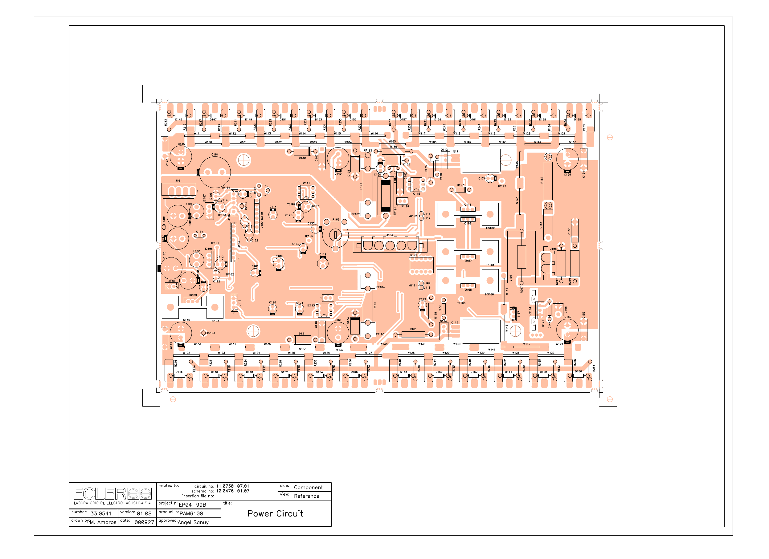
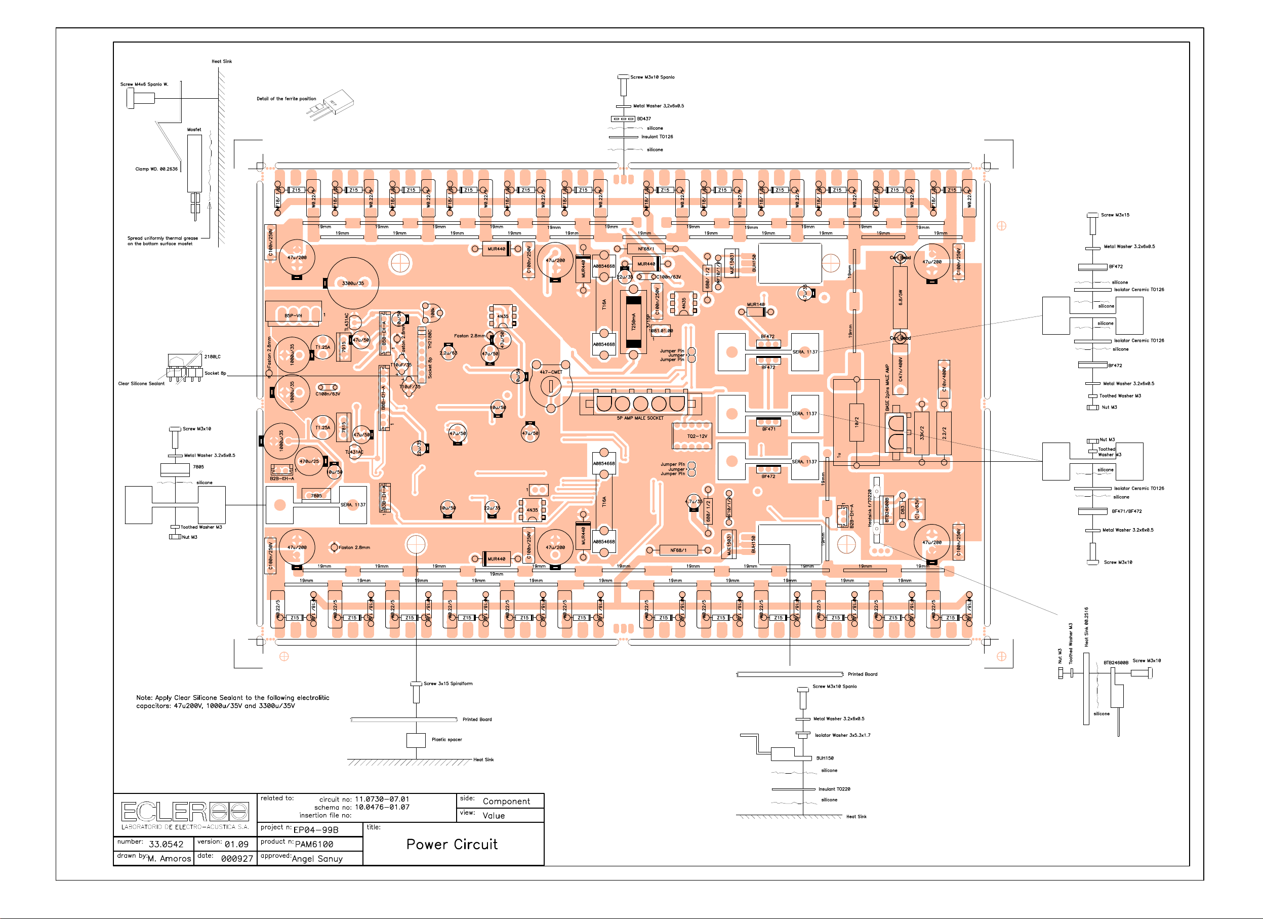
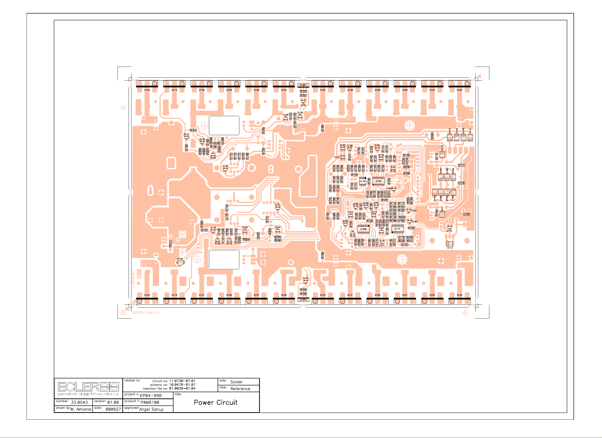
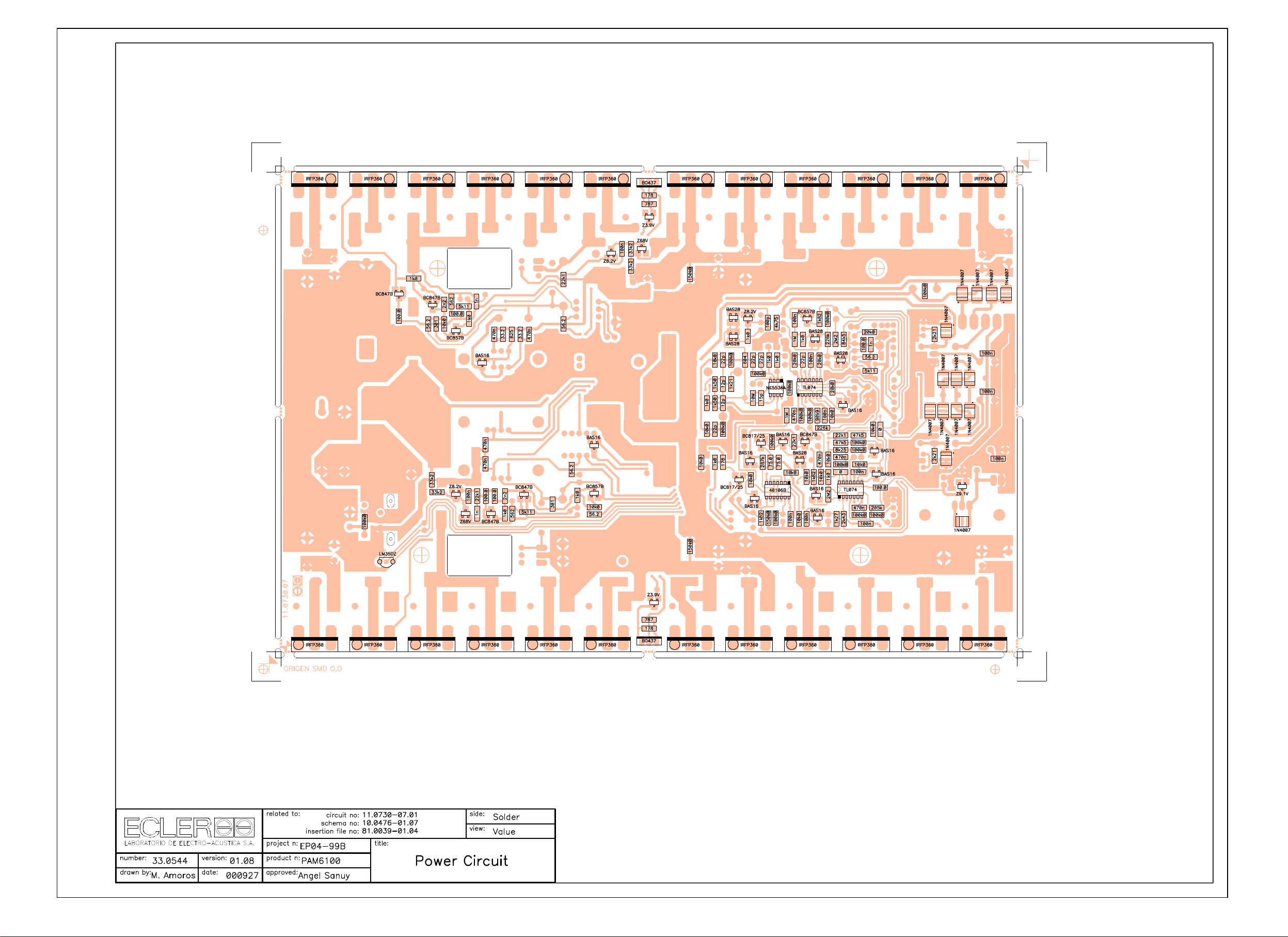
- COMPONENTS LOCATION SCHEMA
AND PARTS LIST
Inputs circuit
Power Amplifier circuit
Soft-Start Power Supply circuit
Potentiometers and leds circuit
Capacitors circuit
Speak on circuit
- TESTING AND QUALITY CONTROL
- TECHNICAL CHARACTERISTICS
- WIRING DIAGRAM
- MECHANICAL DIAGRAM
- PACKING DIAGRAM
PAM4100
- COMPONENTS LOCATION SCHEMA
AND PARTS LIST
Power Amplifier circuit
- MECHANICAL DIAGRAM
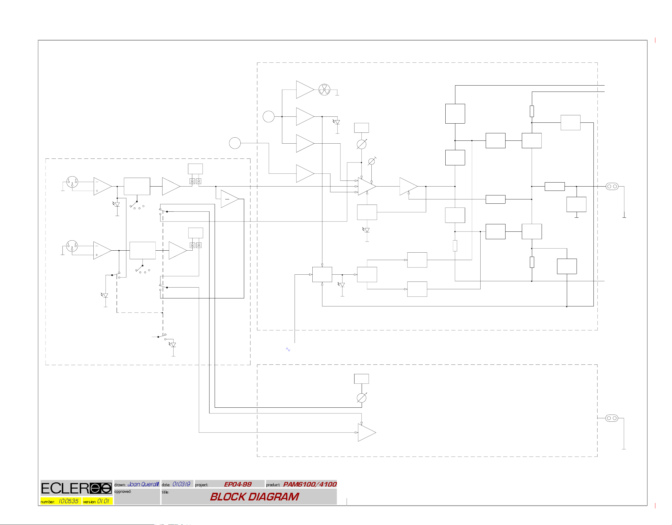
CH 1
OPTIONAL
MODULES
TRANSFORMER
THERMAL
PROBE
MODULE
THERMAL
PROBE
FAN CONTROL
THERMAL PROTECT
THERMAL PROCESSOR
THERMAL PROCESSOR
FAN
++Vcc
+Vcc
WILSON
CURRENT
THERMAL
-Vref
VOLUME
MIRROR
DRIVER MOSFET N
LEVEL
CONVERTER
ADJ 0dB
OVERLOAD
HIGH SIDE
CH 2
INPUT CIRCUIT
HIGH PASS FILTER
STEREO
S.P.
OFF
20Hz
30Hz
40Hz
HIGH PASS FILTER
S.P.
BRIG
OPTIONAL
MODULES
PROTECTION
20Hz
OFF
40Hz
30Hz
AND TIMER
PROTECT
VCA
ANTICLIP
CONTROL
RELAY
CONTROL
FEEDBACK
LEVEL
CONVERTER
DRIVER MOSFET N
CLIP
OUTPUT
SHUTDOWN
OUTPUT
SHUTDOWN
ZOBEL
OUT 1
DC PROTECT
CROWBAR
OVERLOAD
LOW SIDE
-Vcc
POWER MODUL CIRCUIT
+15V
BRIG
AC DETECT
-Vref
VOLUME
OUT 2
VCA
POWER MODUL CIRCUIT

author: Queralt date: 010418 project:
C
E
num:
EPO4-99 Power Module. Functioning description.
structure differs from the design used untill now. This is due to the breakdown voltage
limit on P-channel MosFET's, wich is 200V. This final stage is formed by several
shunted MosFET's, where those of the positive branch are common-drain configured,
and the negative branch are mounted in common-source configuration.
internally compensated in order to obtain gain levels equal or higher than three. The
amplifier's feedback is given by a resistor and a capacitor associated to the operational
amplifier's non inverting input.
Transistors BF587 and BF588 are common-base configured, forming a current supply
structure. This specific transistor type is used because of the higher Vce voltage level
required by this design. They perform simultaneously two functions: they polarize the
MosFET's gate-source junctions, keeping them on the conducting edge, and they
tranfer the OpAmp's output voltage variations referred to signal ground.
LER
52.0010 version: 01.00
Due to the high power level required on the output load, the amplifier final stage's
The system's controlling device is a NE5534-type operational amplifier, wich is
approved:
title:
FUNCTIONING DESCRIPTION
EP04-99
product:
PAM4/6100
The signal variations normally reflected by Q107 and referred to the positive power
supply, are now needed to be floating variations, and referred to the outputs. This
function is done by Q109-110 (BF588), wich are mounted formig a Wilson-type mirror
current supply. This mirror current supply transfers all of the current variations detected
while descending through Q109's collector, to similar variations on Q110's collector
also downward current. Resistors R167 and R174 are used to balance the current
mirror, in order to avoid the use of transistors with forcibly the same beta value. C138
and C141 suppress their resistance when high frequency signal is processed. Diodes
D126 and D127 avoid the transistors to get saturated, and R171 eliminates the loads
on BF588's bases (Baker Circuit).
The system requires about 12Vdc additional voltage upon the usual Vcc level, this
allows a correct saturation and a symetric clipping at the higher MosFET's.
The correct polarization current value is adjusted by a 4K7 potentiometer connected to
the BF transistor's emitter. This adds an additional current to the current source output
on th BF transistor's loading resistors.
In order to maintain the appropiate stand-by current level against varying temperature
conditions, BD437-type transistors are used. As they have a particular temperaturedepending base-emitter voltage curve, this voltage is used to keep a correct voltage
reference for the current supply. As the temperature rises, the reference voltage level
decreases, the gate-source voltage also decreases and, finally, the bias current also
decreases.
52-0010-0100 EP04-99 Anglès.xls 1 of 3

Transistors Q111 and Q112, and their corresponding twins at the lower branch, form
Stand-
a current-buffering circuit wich allows a fast charge and discharge of the power
MosFET's gates.
The Zobel circuit, a resistance-capacitance-inductance formed network associated to
the amplifier's ouput, tries to keep the amplifier's output load impedance constant no
matter wich load value is conected to the output, or wich frequency is processed, in
order to avoid phase shifts on the feedback signal.
To avoid the presence of DC voltage on the output, a diac-triac based system is used,
wich shorts the output to signal ground in case the DC level reaches the diac's
triggering value. To avoid this to happen when processing correct signal (sine
waveform, music...), the diac obtains its reference level from a filtering network formed
by a 100K resistor and a 1mF capacitor.
The protections circuitry overhauls the MosFET's power consumption. Basically, this
circuitry consists of two important sections: MosFET's Id current monitoring, and
MosFET's Vds value detection.
When the MosFET's Id level rises above a certain level, transistor Q119 (controlling
transistor) conducts and decreases the BF transistor's loading resistance, thus reducing
also their gate-source voltage and, finally, lowering the Id current value. This system is
helped by a delayed performance, due to the associated circuitry to Q145 and C174.
This capacitor starts to charge when a current level above the allowed value is
detected, and the protection starts. The greater is the capacitor's charge level, the
higher is also the voltage applied to Q119 controlling transistor's base, increasing its
conduction and, consequently, reducing the gate-source voltage and thus the Id current
value. This system uses a feedback network. The delay used is necessary to avoid
clipping the processed signal's dynamic range, wich should result in the typical clipping
noise. In the negative branch, the protection circuitry is associated to control transistor
Q120.
In case the overcurrent is not ocassional, and persists, after a period of time between
4 and 10 seconds (determined by R142 and C124), the system switches back to
by mode, due to a system-reset. This is done by an optocoupler (IC113) associated to
the negative branch protection circuitry. When protections get activated, IC113
gradually charges C124 untill a 40106-type Schmidt trigger gate switches over . If the
problem persists, this cycle is repeated.
STANDBY CIRCUITRY.
This circuit maintains the Output shutdown relay closed for about 10 seconds, and
thus annulates any current through the MosFET's during this period, just untill the
whole system's power supply voltage reaches its stable level. By this system, we avoid
to hear through the loudspeakers any possible annoying noise proceeding from the
system's start-up.
52-0010-0100 EP04-99 Anglès.xls 2 of 3

This delay time is achieved by using a RC cell, where R135=287K and
40106-
C119=47mF/50V. As this cell charges, its voltage increases untill reaching the
type Schmidt trigger (IC108) switching value; at this point, the relay opens and the
amplifier starts to function normally.
The discharge or reset of capacitor C119=47mF can be done by cutting off the power
supply, or by triggering the Thermal or other protections. During a short period of time,
BC817-type transistor Q102 acts like a switch, shunting two 750 ohm resistors to
C119.
Moreover, the amplifier includes some other additional features, like:
· Volume control by a VCA system.
· An ANTICLIP system.
· A Temperature control system.
The ANTICLIP system. When the amplifier reaches clipping levels, the operational
amplifier looses control on the system's performance and at its output some ±Vcc
voltage peaking pulses may appear, proceeding from its power supply. This peaking
pulses are used to be rectified and sent to an optocoupler (IC111), wich varies the
system's VCA control voltage as a function of those pulse's amplitude, creating a
negative feedback wich should pull back the system into stable functioning area.
The Temperature control system has three main functions:
· Controlling the cooling fan speed, as it is a function of the measured temperature. The
fan's operation voltage range is »7 to 4 Volt.
· Suspending the amplifier's functioning when the temperature exceeds »92ºC
· Reducing the amount of power output, depending on the module's temperature (as it
rises above 85ºC) and on the main power supply's transformer (above 120ºC).
The temperature control system consists on two LM35D-type IC's, wich act like a
thermal probe; one is placed on the amplifier's heat sink, and the other is placed into
the main power supply transformer's core. Moreover, three amplifiers, a comparator
for the thermal probe and a 7805-type IC to feed the cooling fan are used.
The first amplifier (1/4 IC114) acts on the cooling fan speed control. The second
amplifier (1/4 IC114) modifies the VCA gain control, in order to reduce the system's
gain if the temperature rises above 85ºC. The third amplifier (1/4 IC114) modifies the
VCA gain control, in order to reduce the system's gain if the temperature rises above
120ºC. The comparator (1/4 IC114) is responsible for the output shutdown relay
performance, in order to close it as the temperature reaches 92ºC, and thus cutting of
the amplifier's MosFETs bias current. As this happens, the signal output of the whole
unit is cutted off.
52-0010-0100 EP04-99 Anglès.xls 3 of 3


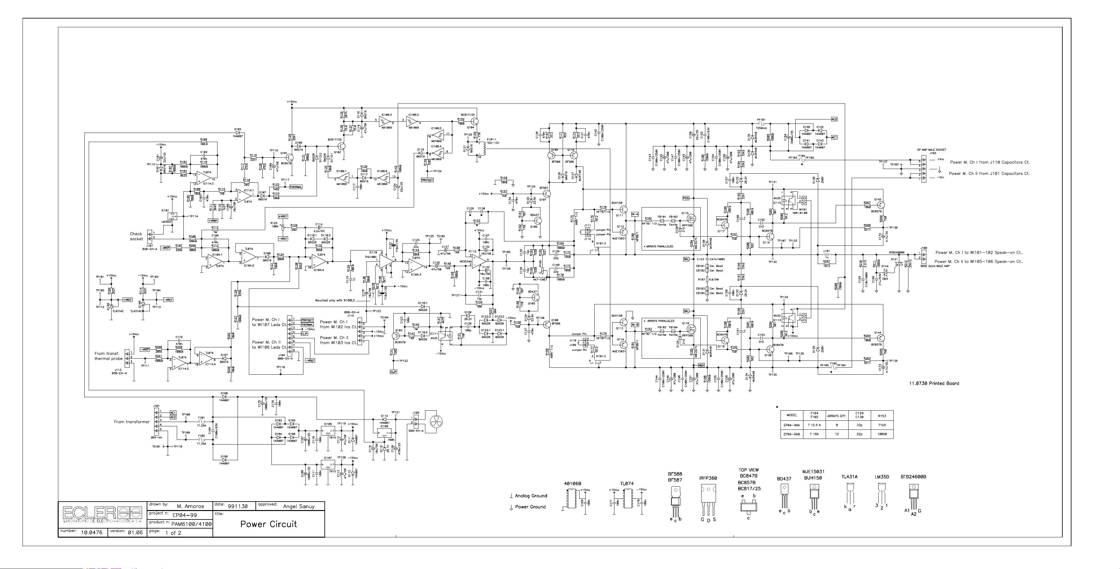


PARTS LIST: PRINTED CIRCUIT 11.0833.04.00
Q
Code
Description
Reference
1
FCCE250470
47u/50
C100
1
FCCE250470
47u/50
C101
1
FCCE250470
47u/50
C102
1
FCCE250470
47u/50
C103
1
FCXCN41000
100n
C104
1
FCXCN41000
100n
C105
1
FCXCN41000
100n
C106
1
FCXCN41000
100n
C107
1
FCXCN41000
100n
C108
1
FCXCN41000
100n
C109
1
FCXCN41000
100n
C110
1
FCXCN41000
100n
C111
1
FCXCN21000
100p
C112
1
FCXCN21000
100p
C113
1
FCXCN21000
100p
C114
1
FCXCN21000
100p
C115
1
FCXCN12201
22p 2%
C116
1
FCXCN12201
22p 2%
C117
1
FCXCN12201
22p 2%
C118
1
FCXCN12201
22p 2%
C119
1
FCCE250100
10u/50
C120
1
FCCE250100
10u/50
C121
1
FCXCN42200
220n
C122
1
FCXCN42200
220n
C123
1
FCXCN42200
220n
C124
1
FCXCN42200
220n
C125
1
FCXCN42200
220n
C126
1
FCXCN42200
220n
C127
1
FCCIPAM833
11.0833 Printed Board
CI100
1
FCXDDBAS28
BAS28
D100
1
FCXDDBAS28
BAS28
D101
1
FCXDDBAS28
BAS28
D102
1
FCXDDBAS28
BAS28
D103
1
FCXDDBAS16
BAS16
D104
1
FCXDDBAS16
BAS16
D105
1
FCIC553200
NE5532AP
IC100
1
FCIC553200
NE5532AP
IC101
1
FCIC072010
TL072
IC102
1
FCIC072010
TL072
IC103
1
FCIC071010
TL071
IC104
1
FCBASX0900
YKF52-5005
J100
1
FCBASX1000
YKF52-5003
J101
1
FCBASX0900
YKF52-5005
J102
1
FCBASX1000
YKF52-5003
J103
1
FCCTM00040
B4B-EH-A
J104
1
FCCTM00070
B7B-EH-A
J152
1
FCCHK00680
68uH
L100
1
FCCHK00680
68uH
L101
1
FCCHK00680
68uH
L102
1
FCCHK00680
68uH
L103
1
FCMJ000100
Jumper
MJ106
1
FCMJ000100
Jumper
MJ107
1
FCXR151000
100k0
R100
1
FCXR151000
100k0
R101
40-0065-0205 EP04-99B.xls 1 of 3

PARTS LIST: PRINTED CIRCUIT 11.0833.04.00
Q
Code
Description
Reference
1
FCXR151000
100k0
R102
1
FCXR151000
100k0
R103
1
FCXR121000
100.0
R104
1
FCXR121000
100.0
R105
1
FCXR121000
100.0
R106
1
FCXR121000
100.0
R107
1
FCXR242430
24k3 0.5%
R108
1
FCXR242430
24k3 0.5%
R109
1
FCXR242430
24k3 0.5%
R110
1
FCXR242430
24k3 0.5%
R111
1
FCXR242430
24k3 0.5%
R112
1
FCXR242430
24k3 0.5%
R113
1
FCXR242430
24k3 0.5%
R114
1
FCXR242430
24k3 0.5%
R115
1
FCXR131000
1k0
R116
1
FCXR131000
1k0
R117
1
FCXR115620
56.2
R118
1
FCXR115620
56.2
R119
1
FCXR131000
1k0
R120
1
FCXR131000
1k0
R121
1
FCXR153400
340k
R122
1
FCXR153400
340k
R123
1
FCXR071000
10M
R124
1
FCXR071000
10M
R125
1
FCXR141820
18k2
R126
1
FCXR141130
11k3
R127
1
FCXR139090
9k09
R128
1
FCXR131500
1k50
R129
1
FCXR141820
18k2
R130
1
FCXR141130
11k3
R131
1
FCXR139090
9k09
R132
1
FCXR131500
1k50
R133
1
FCXR147500
75k0
R134
1
FCXR147500
75k0
R135
1
FCXR144750
47k5
R136
1
FCXR144750
47k5
R137
1
FCXR143650
36k5
R138
1
FCXR143650
36k5
R139
1
FCXR071000
10M
R140
1
FCXR071000
10M
R141
1
FCXR143650
36k5
R142
1
FCXR143650
36k5
R143
1
FCXR242430
24k3 0.5%
R144
1
FCXR242430
24k3 0.5%
R145
1
FCXR141820
18k2
R146
1
FCXR141820
18k2
R147
1
FCXR115620
56.2
R148
1
FCXR115620
56.2
R149
1
FCXR242430
24k3 0.5%
R150
1
FCXR242430
24k3 0.5%
R151
1
FCXR131500
1k50
R152
1
FCINTAP080
NS42J11
S100
1
FCINTD7500
SS050
S101
1
FC6K058460
1058.04.60
WI102
40-0065-0205 EP04-99B.xls 2 of 3

PARTS LIST: PRINTED CIRCUIT 11.0833.04.00
Q
Code
Description
Reference
1
FC6K058460
1058.04.60
WI103
40-0065-0205 EP04-99B.xls 3 of 3

PARTS LIST: PRINTED CIRCUIT 11.0730.07.01
Q
Code
Description
Reference
1
FCCE200220
22u/35
C101
1
FCXCN44700
470n
C102
1
FCXCN44700
470n
C103
1
FCCDK11000
C100n/63V
C104
1
FCXCN44700
470n
C105
1
FCCE250100
10u/50
C106
1
FCCE211000
1000u/35
C107
1
FCCE211000
1000u/35
C108
1
FCCE250470
47u/50
C109
1
FCXCN41000
100n
C110
1
FCXCN41000
100n
C111
1
FCCE250470
47u/50
C112
1
FCCE250470
47u/50
C113
1
FCCE300022
2.2u/63
C114
1
FCXCN40010
1n
C115
1
FCCE250100
10u/50
C116
1
FCXCN41000
100n
C117
1
FCCE250100
10u/50
C118
1
FCCE250470
47u/50
C119
1
FCCE154700
470u/25
C120
1
FCCG001000
T10uF/35
C121
1
FCCG001000
T10uF/35
C122
1
FCXCN41000
100n
C123
1
FCCE200220
22u/35
C124
1
FCXCN12200
22p
C125
1
FCCE250470
47u/50
C126
1
FCCE250470
47u/50
C127
1
FCXCN21000
100p
C128
1
FCXCN12200
22p
C129
1
FCXCN12200
22p
C130
1
FCXCN11500
15p
C131
1
FCCE250100
10u/50
C132
1
FCCE250100
10u/50
C133
1
FCXCN44700
470n
C134
1
FCXCN11200
12p
C135
1
FCXCN11200
12p
C136
1
FCXCN44700
470n
C137
1
FCXCN44700
470n
C138
1
FCXCN12200
22p
C139
1
FCXCN12200
22p
C140
1
FCXCN44700
470n
C141
1
FCCDN11000
C100n/250V
C142
1
FCCDN11000
C100n/250V
C143
1
FCCDN11000
C100n/250V
C144
1
FCCE350047
47u/200
C145
1
FCCE350047
47u/200
C146
1
FCCDN11000
C100n/250V
C147
1
FCCDN11000
C100n/250V
C148
1
FCCE350047
47u/200
C149
1
FCCE200220
22u/35
C150
1
FCCE350047
47u/200
C151
1
FCCDK11000
C100n/63V
C152
1
FCCDH71047
C47n/400V
C153
1
FCCDN11000
C100n/250V
C154
1
FCCDN11000
C100n/250V
C155
1
FCCE350047
47u/200
C156
40-0065-0206 EP04-99B.xls 1 of 11

PARTS LIST: PRINTED CIRCUIT 11.0730.07.01
Q
Code
Description
Reference
1
FCXCN41000
100n
C157
1
FCXCN41000
100n
C158
1
FCCE350047
47u/200
C159
1
FCXCN40010
1n
C160
1
FCXCN40010
1n
C161
1
FCXCN40022
2n2
C162
1
FCXCN40022
2n2
C163
1
FCCE213300
3300u/35
C164
1
FCCDH71011
C10n/400V
C165
1
FCCDK20010
C1u/63V
C166
1
FCXCN41000
100n
C167
1
FCXCN41000
100n
C168
1
FCXCN41000
100n
C169
1
FCXCN41000
100n
C170
1
FCXCN41000
100n
C171
1
FCXCN44700
470n
C172
1
FCCE200047
4.7u/35
C173
1
FCCE200047
4.7u/35
C174
1
FCCE211000
1000u/35
C175
1
FCXCN41000
100n
C176
1
FCPERL2550
Cer. Bead
CB101
1
FCPERL2550
Cer. Bead
CB102
1
FCPERL2550
Cer. Bead
CB103
1
FCPERL2550
Cer. Bead
CB104
1
FCCIPAM730
11.0730 Printed Board
CI101
1
FCXDDBAS16
BAS16
D101
1
FCXDD40070
1N4007
D102
1
FCXDD40070
1N4007
D103
1
FCXDD40070
1N4007
D104
1
FCXDD40070
1N4007
D105
1
FCXDD40070
1N4007
D106
1
FCXDDBAS16
BAS16
D107
1
FCXDDBAS16
BAS16
D108
1
FCXDDBAS16
BAS16
D109
1
FCXDDBAS28
BAS28
D110
1
FCXDD40070
1N4007
D111
1
FCXDD40070
1N4007
D112
1
FCXDDBAS28
BAS28
D113
1
FCXDD40070
1N4007
D114
1
FCXZ000091
Z9.1V
D115
1
FCXDDBAS16
BAS16
D116
1
FCXDDBAS16
BAS16
D117
1
FCXDDBAS28
BAS28
D118
1
FCXDDBAS16
BAS16
D119
1
FCXZ000082
Z8.2V
D120
1
FCXDDBAS16
BAS16
D121
1
FCXDDBAS28
BAS28
D122
1
FCXDDBAS28
BAS28
D123
1
FCXZ000039
Z3.9V
D124
1
FCXZ000039
Z3.9V
D125
1
FCXDDBAS16
BAS16
D126
1
FCDDMUR140
MUR140
D127
1
FCDD041500
Z15
D128
1
FCDD041500
Z15
D129
1
FCDDMUR440
MUR440
D130
1
FCDDMUR440
MUR440
D131
40-0065-0206 EP04-99B.xls 2 of 11

PARTS LIST: PRINTED CIRCUIT 11.0730.07.01
Q
Code
Description
Reference
1
FCXZ000082
Z8.2V
D132
1
FCXZ000082
Z8.2V
D133
1
FCDDMUR440
MUR440
D134
1
FCDDMUR440
MUR440
D135
1
FCDDMUR440
MUR440
D136
1
FCXZ000680
Z68V
D138
1
FCXZ000680
Z68V
D139
1
FCXDD40070
1N4007
D140
1
FCXDD40070
1N4007
D141
1
FCXDD40070
1N4007
D142
1
FCXDD40070
1N4007
D143
1
FCDIDB3000
DB3
D144
1
FCDD041500
Z15
D145
1
FCDD041500
Z15
D146
1
FCDD041500
Z15
D147
1
FCDD041500
Z15
D148
1
FCDD041500
Z15
D149
1
FCDD041500
Z15
D150
1
FCDD041500
Z15
D151
1
FCDD041500
Z15
D152
1
FCDD041500
Z15
D153
1
FCDD041500
Z15
D154
1
FCDD041500
Z15
D155
1
FCDD041500
Z15
D156
1
FCDD041500
Z15
D157
1
FCDD041500
Z15
D158
1
FCDD041500
Z15
D159
1
FCDD041500
Z15
D160
1
FCDD041500
Z15
D161
1
FCDD041500
Z15
D162
1
FCDD041500
Z15
D163
1
FCDD041500
Z15
D164
1
FCDD041500
Z15
D165
1
FCDD041500
Z15
D166
1
FCXDDBAS16
BAS16
D167
1
FCXDD40070
1N4007
D168
1
FCXDD40070
1N4007
D169
1
FCFUS40125
T1.25A
F101
1
FCFUS40125
T1.25A
F102
1
FCFUS50080
T250mA
F103
1
FCFUS60400
T16A
F104
1
FCFUS60400
T16A
F105
1
FCFER43220
Ferrite
FB101
1
FCFER43220
Ferrite
FB102
1
FCFER43220
Ferrite
FB103
1
FCFER43220
Ferrite
FB104
1
FCFER43220
Ferrite
FB105
1
FCFER43220
Ferrite
FB106
1
FCFER43220
Ferrite
FB107
1
FCFER43220
Ferrite
FB108
1
FCFER43220
Ferrite
FB109
1
FCFER43220
Ferrite
FB110
1
FCFER43220
Ferrite
FB111
1
FCFER43220
Ferrite
FB112
1
FCFER43220
Ferrite
FB113
1
FCFER43220
Ferrite
FB114
40-0065-0206 EP04-99B.xls 3 of 11

PARTS LIST: PRINTED CIRCUIT 11.0730.07.01
Q
Code
Description
Reference
1
FCFER43220
Ferrite
FB115
1
FCFER43220
Ferrite
FB116
1
FCFER43220
Ferrite
FB117
1
FCFER43220
Ferrite
FB118
1
FCFER43220
Ferrite
FB119
1
FCFER43220
Ferrite
FB120
1
FCFER43220
Ferrite
FB121
1
FCFER43220
Ferrite
FB122
1
FCFER43220
Ferrite
FB123
1
FCFER43220
Ferrite
FB124
1
FCFER43220
Ferrite
FB125
1
FCFER43220
Ferrite
FB126
1
FCFER43220
Ferrite
FB127
1
FCFER43220
Ferrite
FB128
1
FCFER43220
Ferrite
FB129
1
FCFER43220
Ferrite
FB130
1
FCFER43220
Ferrite
FB131
1
FCFER43220
Ferrite
FB132
1
FCFER43220
Ferrite
FB133
1
FCFER43220
Ferrite
FB134
1
FCFER43220
Ferrite
FB135
1
FCFER43220
Ferrite
FB136
1
FCFER43220
Ferrite
FB137
1
FCFER43220
Ferrite
FB138
1
FCFER43220
Ferrite
FB139
1
FCFER43220
Ferrite
FB140
1
FCFER43220
Ferrite
FB141
1
FCFER43220
Ferrite
FB142
1
FCFER43220
Ferrite
FB143
1
FCFER43220
Ferrite
FB144
1
FCFER43220
Ferrite
FB145
1
FCFER43220
Ferrite
FB146
1
FCFER43220
Ferrite
FB147
1
FCFER43220
Ferrite
FB148
1
FCRAD12636
SERA. 1137
HS100
1
FCRAD12636
SERA. 1137
HS101
1
FCRAD12636
SERA. 1137
HS102
1
FCRAD12636
SERA. 1137
HS103
1
FCMECT0220
Heatsink f/TO220
HS104
1
FCRAD03000
Heatsink f/ Power Module
HS105
1
FCRAD03000
Heatsink f/ Power Module
HS106
1
FCIC350000
LM35DZ
IC101
1
FCIC431000
TL431AC
IC102
1
FCIC074010
TL074
IC104
1
FCIC431000
TL431AC
IC105
1
FCREG78150
7815
IC106
1
FCREG79150
7915
IC107
1
FCIC401060
40106B
IC108
1
FCREG78050
7805
IC109
1
FCIC218000
TH2180C
IC110
1
FCIC435000
4N35
IC111
1
FCIC553410
NE5534A
IC112
1
FCIC435000
4N35
IC113
1
FCIC074010
TL074
IC114
1
FCIC435000
4N35
IC115
1
FCMICTO126
Insulant TO126
IN100
40-0065-0206 EP04-99B.xls 4 of 11

PARTS LIST: PRINTED CIRCUIT 11.0730.07.01
Q
Code
Description
Reference
1
FCMICTO126
Insulant TO126
IN101
1
FCMICTO220
Insulant TO220
IN102
1
FCMICTO220
Insulant TO220
IN103
1
FCTERM0080
Socket 8p
J100
1
FCCTJ10050
B5P-VH
J101
1
FCCTAMP050
5P AMP MALE SOCKET
J103
1
FCCTM00080
B8B-EH-A
J104
1
FCCTM00020
B2B-EH-A
J105
1
FCCTM00020
B2B-EH-A
J107
1
FCCTAMP020
BASE 2pins MALE AMP
J108
1
FCTERM0100
Jumper Pin
J109
1
FCTERM0100
Jumper Pin
J110
1
FCTERM0100
Jumper Pin
J111
1
FCTERM0100
Jumper Pin
J112
1
FCCTM00030
B3B-EH-A
J113
1
FCCTM00050
B5B-EH-A
J115
1
FCREL00300
TQ2-12V
K101
1
FCIND00100
1u
L101
1
FCMJ000100
Jumper
MJ101
1
FCMJ000100
Jumper
MJ102
1
FCPINZAM00
Clamp WD. 00.2636
MP100
1
FCPINZAM00
Clamp WD. 00.2636
MP101
1
FCPINZAM00
Clamp WD. 00.2636
MP102
1
FCPINZAM00
Clamp WD. 00.2636
MP103
1
FCTUE00300
Nut M3
NV100
1
FCTUE00300
Nut M3
NV101
1
FCTUE00300
Nut M3
NV102
1
FCTUE00300
Nut M3
NV103
1
FCTUE00300
Nut M3
NV104
1
FCPORF3150
3/15P
PF101
1
FCPORF0100
A0854668
PF102
1
FCPORF0100
A0854668
PF103
1
FCPORF0100
A0854668
PF104
1
FCPORF0100
A0854668
PF105
1
FCXTT08470
BC847B
Q101
1
FCXTT08170
BC817/25
Q102
1
FCXTT08570
BC857B
Q103
1
FCXTT08170
BC817/25
Q104
1
FCTR437000
BD437
Q105
1
FCTR437000
BD437
Q106
1
FCTR471000
BF471
Q107
1
FCTR472000
BF472
Q108
1
FCTR472000
BF472
Q109
1
FCTR472000
BF472
Q110
1
FCTR150000
BUH150
Q111
1
FCTR150310
MJE15031
Q112
1
FCTR150000
BUH150
Q113
1
FCTR150310
MJE15031
Q114
1
FCTR360000
IRFP360
Q115
1
FCTR360000
IRFP360
Q116
1
FCXTT08470
BC847B
Q117
1
FCXTT08470
BC847B
Q118
1
FCXTT08470
BC847B
Q119
1
FCXTT08470
BC847B
Q120
1
FCTI246000
BTB24600B
Q121
1
FCTR360000
IRFP360
Q122
40-0065-0206 EP04-99B.xls 5 of 11

PARTS LIST: PRINTED CIRCUIT 11.0730.07.01
Q
Code
Description
Reference
1
FCTR360000
IRFP360
Q123
1
FCTR360000
IRFP360
Q124
1
FCTR360000
IRFP360
Q125
1
FCTR360000
IRFP360
Q126
1
FCTR360000
IRFP360
Q127
1
FCTR360000
IRFP360
Q128
1
FCTR360000
IRFP360
Q129
1
FCTR360000
IRFP360
Q130
1
FCTR360000
IRFP360
Q131
1
FCTR360000
IRFP360
Q132
1
FCTR360000
IRFP360
Q133
1
FCTR360000
IRFP360
Q134
1
FCTR360000
IRFP360
Q135
1
FCTR360000
IRFP360
Q136
1
FCTR360000
IRFP360
Q137
1
FCTR360000
IRFP360
Q138
1
FCTR360000
IRFP360
Q139
1
FCTR360000
IRFP360
Q140
1
FCTR360000
IRFP360
Q141
1
FCTR360000
IRFP360
Q142
1
FCTR360000
IRFP360
Q143
1
FCXTT08570
BC857B
Q144
1
FCXTT08570
BC857B
Q145
1
FCXR151000
100k0
R101
1
FCXR151000
100k0
R102
1
FCXR138250
8k25
R103
1
FCXR132210
2k21
R104
1
FCXR141000
10k0
R105
1
FCXR151000
100k0
R106
1
FCXR152260
226k
R107
1
FCXR141000
10k0
R108
1
FCXR121000
100.0
R109
1
FCXR151000
100k0
R110
1
FCXR132430
2k43
R111
1
FCXR061000
1M
R112
1
FCXR151000
100k0
R113
1
FCXR132210
2k21
R114
1
FCXR131000
1k0
R115
1
FCXR131270
1k27
R116
1
FCXR144750
47k5
R117
1
FCXR062200
2M2
R118
1
FCXR142210
22k1
R119
1
FCXR144750
47k5
R120
1
FCXR141000
10k0
R121
1
FCXR131820
1k82
R122
1
FCXR141000
10k0
R123
1
FCXR142000
20k0
R124
1
FCRJC61000
100k
R125
1
FCXR152260
226k
R126
1
FCXR151000
100k0
R127
1
FCXR142210
22k1
R128
1
FCXR062200
2M2
R129
1
FCXR148450
84k5
R130
1
FCXR151000
100k0
R131
1
FCXR142000
20k0
R132
1
FCXR141000
10k0
R133
40-0065-0206 EP04-99B.xls 6 of 11
Loading...