Diodes PAM8303C User Manual
A
f
Description
The PAM8303C is a 3W mono filterless Class-D amplifier with high
PSRR and differential input that eliminate noise and RF rectification.
Features like 90% efficiency and small PCB area make the
PAM8303C Class-D amplifier ideal for cellular handsets. The filterless
architecture requires no external output filter, fewer external
components, less PCB area and lower system costs, and simplifies
application design.
The PAM8303C features short circuit protection and thermal
shutdown.
The PAM8303C is available in 9-ball WCSP, MSOP-8 and DFN 3x3
8-pin packages.
MONO CLASS-D AUDIO POWER AMPLIFIER
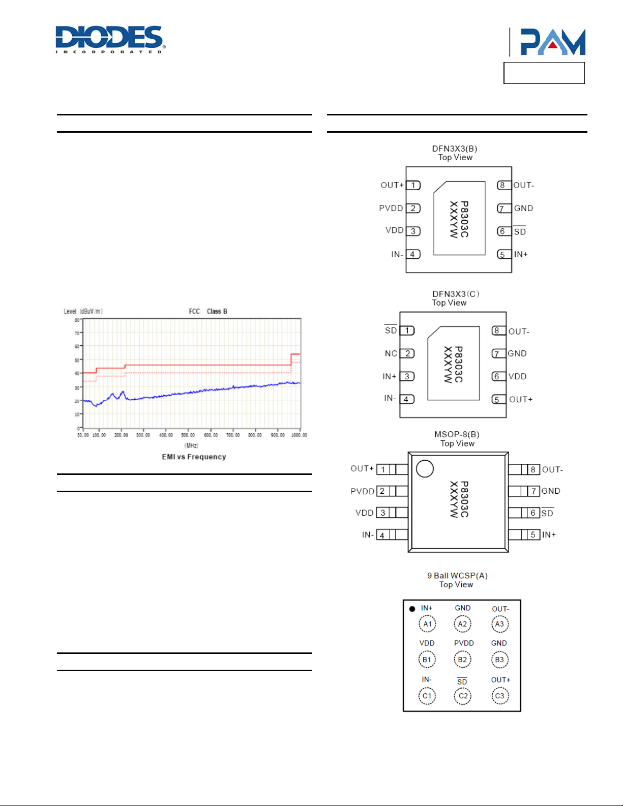
Pin Assignments
Product Line o
Diodes Incorporated
PAM8303C
ULTRA LOW EMI, 3W FILTERLESS
Features
Ultra Low EMI, -20dB Better Than FCC Class-B @ 300MHz
High Efficiency up to 90% @1W with an 8Ω Speaker
Shutdown Current <1µA
3W@10% THD Output with a 4Ω Load at 5V Supply
Demanding Few External Components
Superior Low Noise without Input
Supply Voltage from 2.8V to 5.5V
Short Circuit Protection
Thermal Shutdown
Available in Space Saving Packages: 1.45mmx1.45mm
WCSP9, MSOP-8, DFN3x3-8
Pb-Free Package
Applications
Cellular Phones/Smart Phones
MP4/MP3
GPS
Digital Photo Frame
Electronic Dictionary
Portable Game Machines
PAM8303C
Document number: DSxxxxx Rev. 1 - 2
www.diodes.com
1 of 17
June 2013
© Diodes Incorporated
A
f
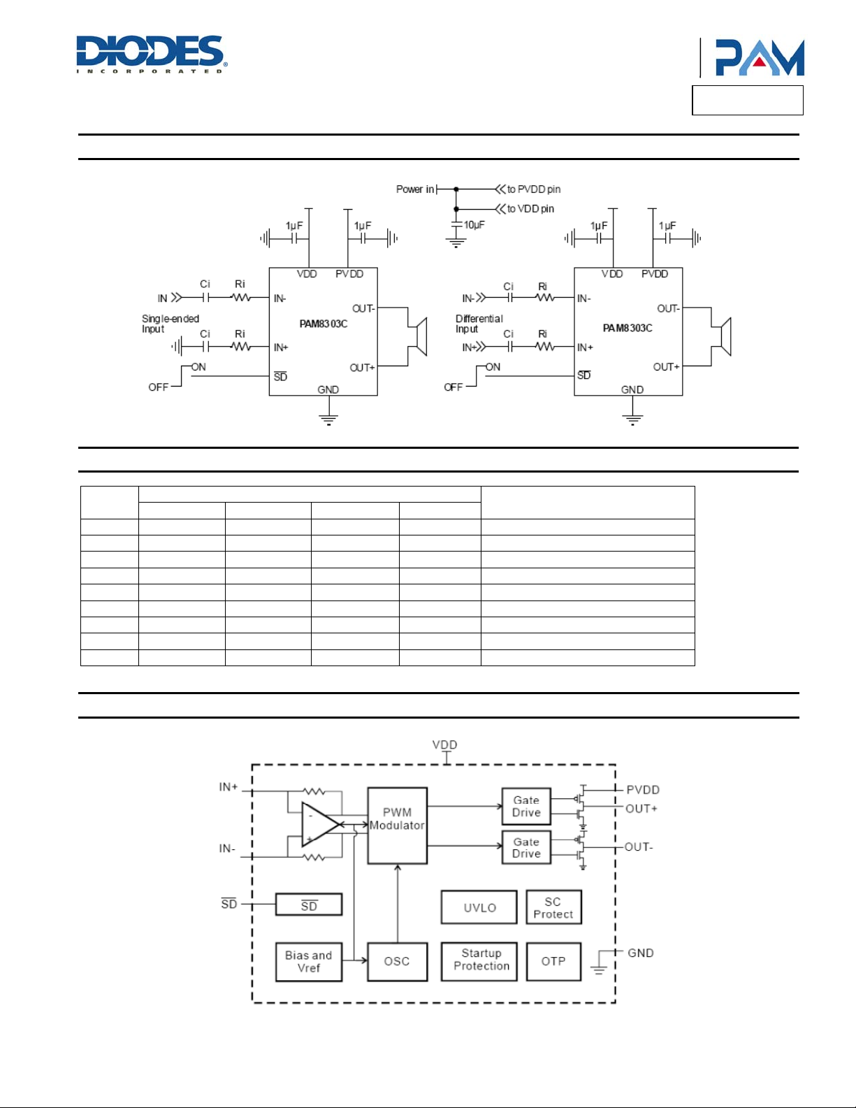
Typical Applications Circuit
Product Line o
Diodes Incorporated
PAM8303C
Pin Descriptions
Pin
Name
OUT+ C3 1 5 1 Positive BTL Output
PVDD B2 2 — 2 Power Supply
VDD B1 3 6 3 Analog Power Supply
IN- C1 4 4 4 Negative Differential Input
IN+ A1 5 3 5 Positive Differential Input
SD C2 6 1 6 Shutdown Terminal (active low)
GND A2, B3 7 7 7 Ground
OUT- A3 8 8 8 Negative BTL Output
NC — — 2 —
WCSP(A) DFN3X3-8 (B) DFN3X3-8 (C) MSOP-8 (B)
Pin Name
Function
Functional Block Diagram
PAM8303C
Document number: DSxxxxx Rev. 1 - 2
2 of 17
www.diodes.com
June 2013
© Diodes Incorporated
A
f
Product Line o
Diodes Incorporated
PAM8303C
Absolute Maximum Ratings (@T
These are stress ratings only and functional operation is not implied. Exposure to absolute maximum ratings for prolonged time periods may
affect device reliability. All voltages are with respect to ground.
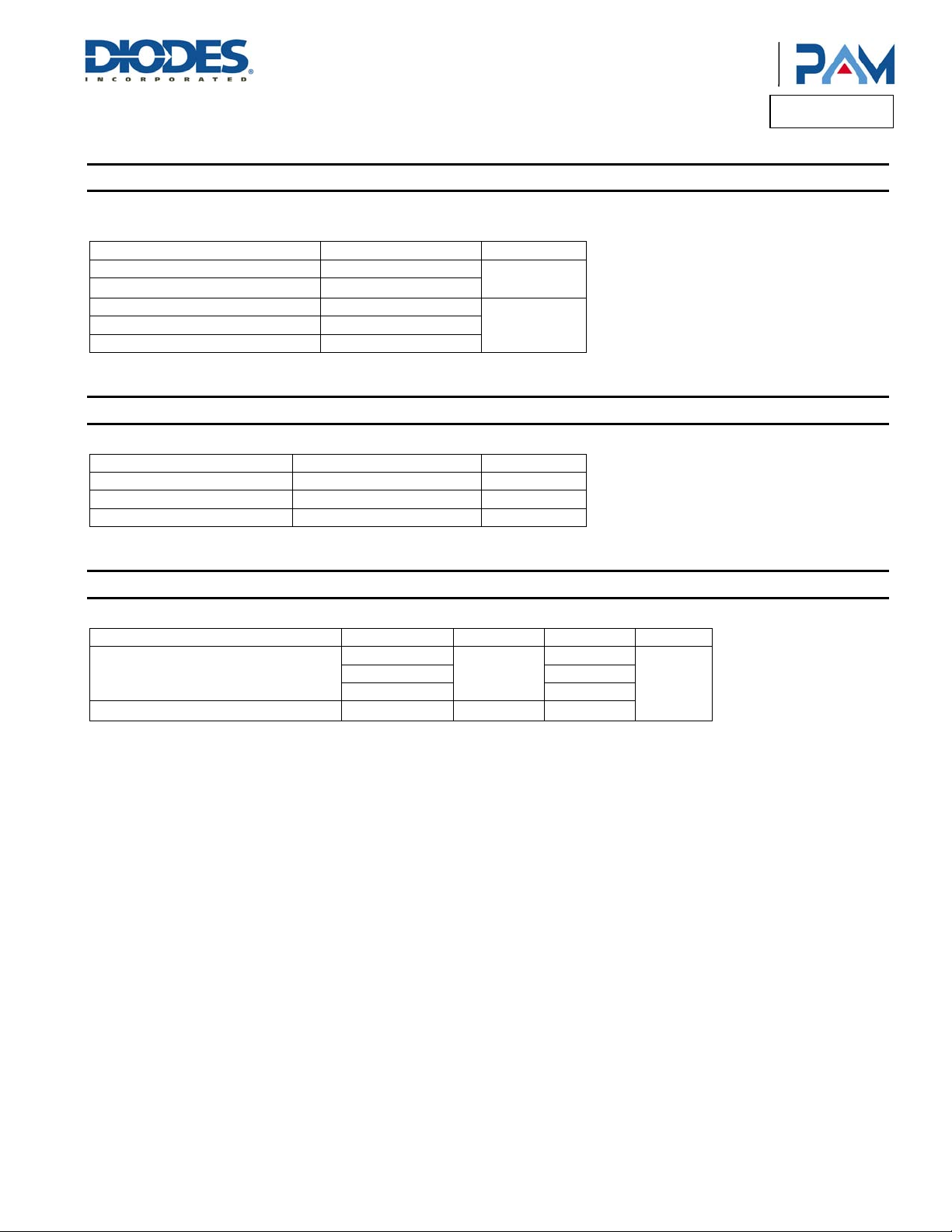
Parameter Rating Unit
Supply Voltage 6.0
Input Voltage
Maximum Junction Temperature 150
Storage Temperature -65 to +150
Soldering Temperature 250, 10 sec
Recommended Operating Conditions (@T
Parameter Rating Unit
Supply Voltage Range 2.8 to 5.5 V
Ambient Temperature Range -40 to +85 °C
Junction Temperature Range -40 to +125 °C
= +25°C, unless otherwise specified.)
A
-0.3 to V
DD
+0.3
= +25°C, unless otherwise specified.)
A
V
°C
Thermal Information
Parameter Package Symbol Max Unit
WCSP 1.45x1.45
Thermal Resistance (Junction to Ambient)
Thermal Resistance (Junction to Case) MSOP-8
Note: For the 9-pin CSP package, the thermal resistance is highly dependent on the PCB heat sink area.
For example, the Θ
using ground and power planes, the value is around 90°C/W.
can equal to 195°C/W with 50mm2 total area or 135°C/W with 500mm2 area. When
ja
PAM8303C
Document number: DSxxxxx Rev. 1 - 2
MSOP-8 180
DFN3x3-8 47.9
www.diodes.com
θ
JA
θ
JC
3 of 17
90-220
75
°C/W
June 2013
© Diodes Incorporated
A
f
Product Line o
Diodes Incorporated
PAM8303C
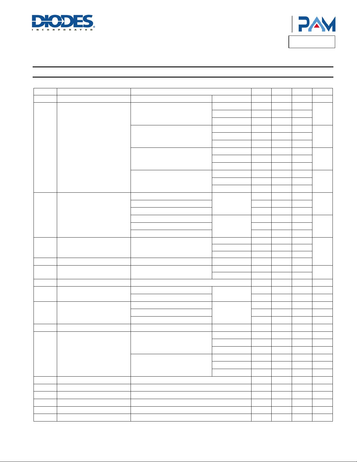
Electrical Characteristics (@T
Symbol Parameter Test Conditions Min Typ Max Units
VDD
PO
THD+N
PSRR Power Supply Ripple Rejection
Dyn Dynamic Range
VN
CMRR Common Mode Rejection Ratio
ISD
R
DS(ON)
RIN
fSW
GV
VOS
VIH
VIL
Supply Voltage
Output Power
Total Harmonic Distortion Plus
Noise
Output Noise Inputs AC-Grounded
η Peak Efficiency
Quiescent Current
IQ
Shutdown Current
Static Drain-to-Source
On-State Resistor
Input Resistance
Switching Frequency
Closed Loop Gain
Output Offset Voltage
Enable Input High Voltage
Enable Input Low Voltage
= +25°C, VDD = 5V, Gain = 2V/V, RL = L(33µH) + R + L(33µH), unless otherwise specified.)
A
THD+N = 10%, f = 1KHz, R = 4Ω
THD+N = 1%, f = 1KHz, R = 4Ω
THD+N = 10%, f = 1KHz, R = 8Ω
THD+N = 1%, f = 1KHz, R = 8Ω
= 5.0V, PO = 1W, R = 8Ω
V
DD
VDD = 3.6V, PO = 0.1W, R = 8Ω
VDD = 3.2V, PO = 0.1W, R = 8Ω
VDD = 5.0V, PO = 0.5W, R = 4Ω
VDD = 3.6V, PO = 0.2W, R = 4Ω
VDD = 3.2V, PO = 0.1W, R = 4Ω
V
= 3.6V, Inputs AC-Grounded
DD
with C
= 1µF
IN
V
= 5V, THD = 1%, R = 8Ω
DD
= 5.0V
V
DD
VDD = 3.6V
VDD = 3.2V
V
= 5.0V
DD
VDD = 3.6V
VDD = 3.2V
V
= 5.0V
DD
VDD = 3.6V
VDD = 3.2V
= 5.0V
V
DD
VDD = 3.6V
VDD = 3.2V
f = 1kHz
f = 1kHz
f = 217Hz -63 -55
f = 1kHz -62 -55
f = 10kHz -52 -40
f = 1kHz 85 95
2.8 5.5 V
2.85 3.00
1.65 1.80
1.20 1.35
2.50 2.66
1.15 1.30
0.85 1.0
1.65 1.8
0.75 0.9
0.55 0.7
1.3 1.5
0.55 0.72
0.40 0.55
0.28 0.35
0.40 0.45
0.55 0.60
0.20 0.25
0.35 0.40
0.5 0.55
No A-Weighting 50 100
A-Weighting 30 60
V
= 100m, VPP, f =1kHz
IC
= 8Ω, THD = 10%
R
L
RL = 4Ω, THD = 10%
= 5.0V
V
DD
VDD = 3.6V
f = 1kHz
R = 8Ω
VDD = 3.0V
VDD = 3.0V to 5.0V VSD = 0.3V
V
= 5.0V
CSP Package, High Side PMOS
plus Low Side NMOS,
I = 500mA
MSOP/DFN package,
High Side PMOS plus
Low Side NMOS, I = 500mA
DD
VDD = 3.6V
VDD = 3.0V
V
= 5.0V
DD
VDD = 3.6V
VDD = 3.0V
VDD = 3V to 5V
VDD = 3V to 5V
Input AC-Ground, VDD = 5V
VDD = 5V
VDD = 5V
40 63 dB
85 90
80 86 %
7.5 10
4.6 7
3.6 5 mA
0.5 2 µA
280 350
300 375
325 400
365 420
385 450
410 500
150 KΩ
200 250 300 KHz
300kΩ/R
dB
I
10 50 mV
1.5 V
0.3 V
W
W
W
W
%
%
dB
µV
PAM8303C
Document number: DSxxxxx Rev. 1 - 2
4 of 17
www.diodes.com
June 2013
© Diodes Incorporated
A
f
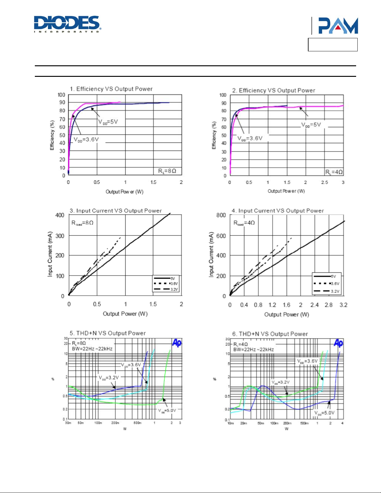
Typical Performance Characteristics (@T
Product Line o
Diodes Incorporated
PAM8303C
= +25°C, VDD = 5V, f = 1kHz, Gain = 2V/V, unless otherwise specified.)
A
PAM8303C
Document number: DSxxxxx Rev. 1 - 2
5 of 17
www.diodes.com
© Diodes Incorporated
June 2013
A
f
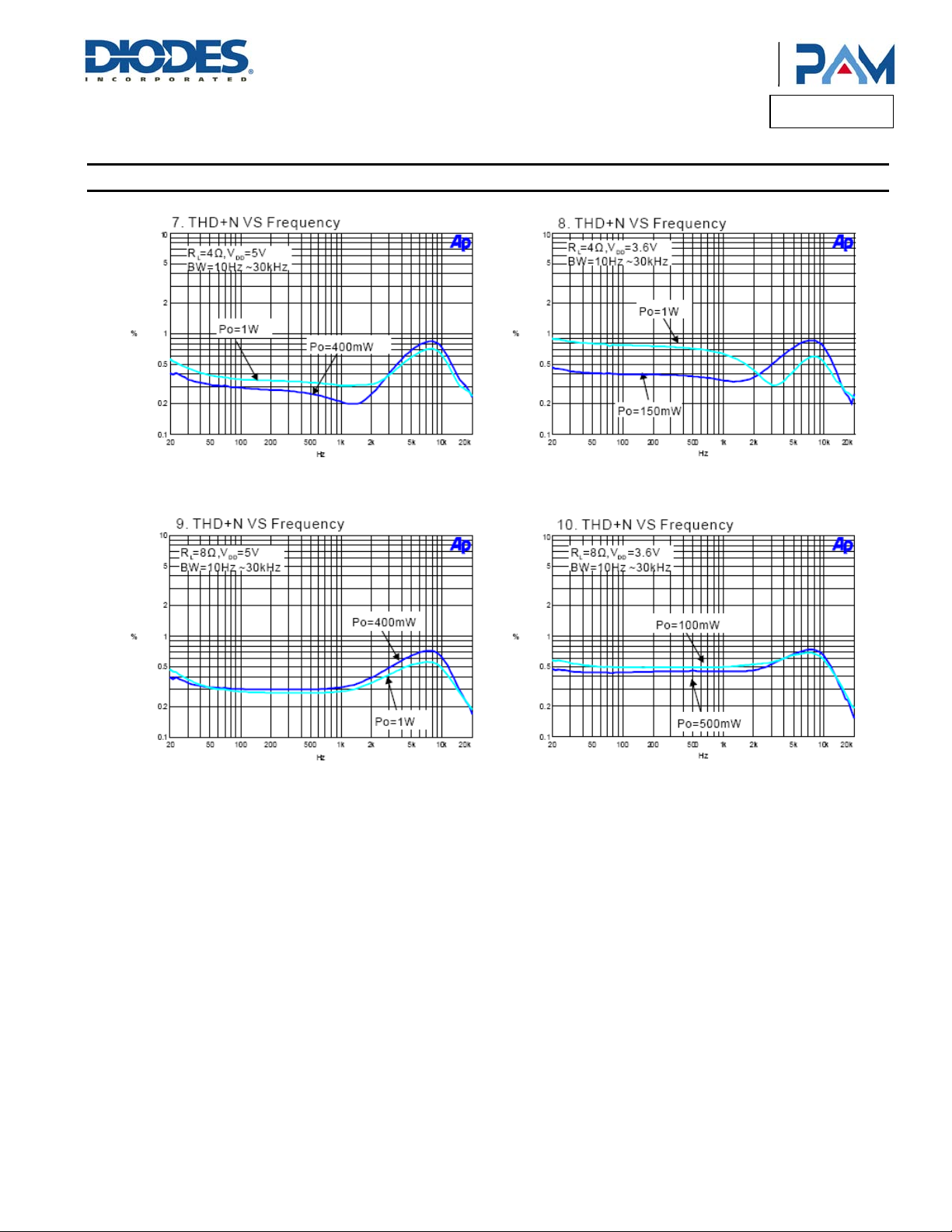
Typical Performance Characteristics (cont.) (@T
Product Line o
Diodes Incorporated
PAM8303C
= +25°C, VDD = 5V, f = 1kHz, Gain = 2V/V, unless otherwise specified.)
A
PAM8303C
Document number: DSxxxxx Rev. 1 - 2
6 of 17
www.diodes.com
© Diodes Incorporated
June 2013
 Loading...