Diodes PAM8004 User Manual

A
f
Description
The PAM8004 is a 3Wm Class-D audio amplifier. It offers low
THD+N, allowing it to achieve high quality sound reproduction. The
new filterless architecture allows the device to drive the speaker
directly, requiring no low-pass output filters, in order to save system
cost and PCB area.
With the same numbers of external components, the efficiency of the
PAM8004 is much better than that of Class-AB cousins. It can extend
the battery life, ideal for portable applications
The PAM8004 is available in SOP-16L package.
Features
3W Output at 10% THD with a 3 Load and
5V Power Supply
2.5W Output at 10% THD with a 4 Load and 5V Power Supply
Filterless, Low Quiescent Current and Low EMI
Low THD+N
Superior Low Noise
Short Circuit Protection
Thermal Shutdown
Few External Components to Save the Space and Cost
Pb-Free Package
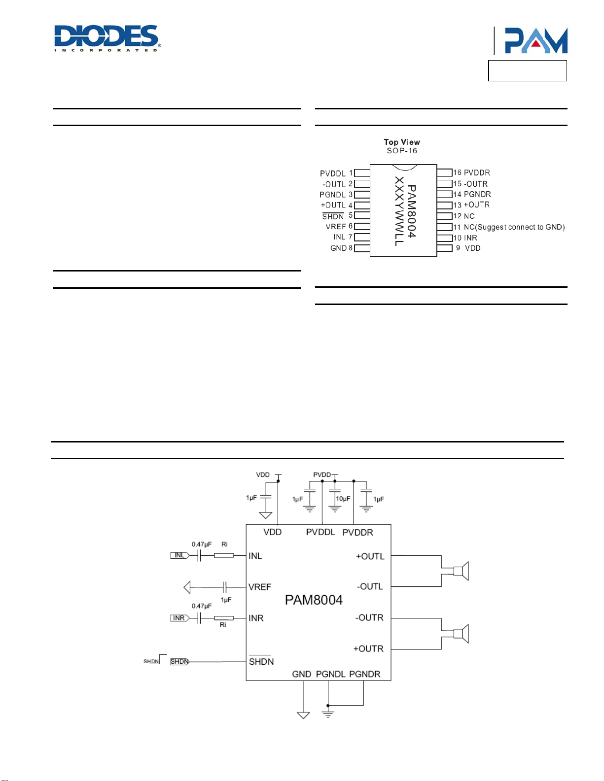
Typical Applications Circuit
Product Line o
Diodes Incorporated
PAM8004
FILTERLESS 3W CLASS-D STEREO AUDIO AMPLIFIER
Pin Assignments
Applications
Portable Speakers
LCD Monitors / TV
Notebook Computers
Portable DVD Players, Game Machines
PAM8004
Document number: DSxxxxx Rev. 1 - 0
1 of 11
www.diodes.com
November 2012
© Diodes Incorporated

A
f
Pin Descriptions
Pin
Number
1 PVDDL
2 -OUTL
3 PGNDL
4 +OUTL
5 SHDN
6 VREF
7 INL
8 GND
9 VDD
10 INR
11 NC
12 NC
13 +OUTR
14 PGNDR
15 -OUTR
16 PVDDR
Pin
Name
Left Channel Power Supply
Left Channel Negative Output
Left Channel Power GND
Left Channel Positive Output
Shutdown Control Input (active low)
Internal Analog Reference, Connect a Bypass Capacitor from VREF to GND
Left Channel Input
Analog Ground
Analog Power Supply
Right Channel Input
Not Connected (Suggest Connect to GND)
Not Connected
Right Channel Positive Output
Right Channel Power GND
Right Channel Negative Output
Right Channel Power Supply
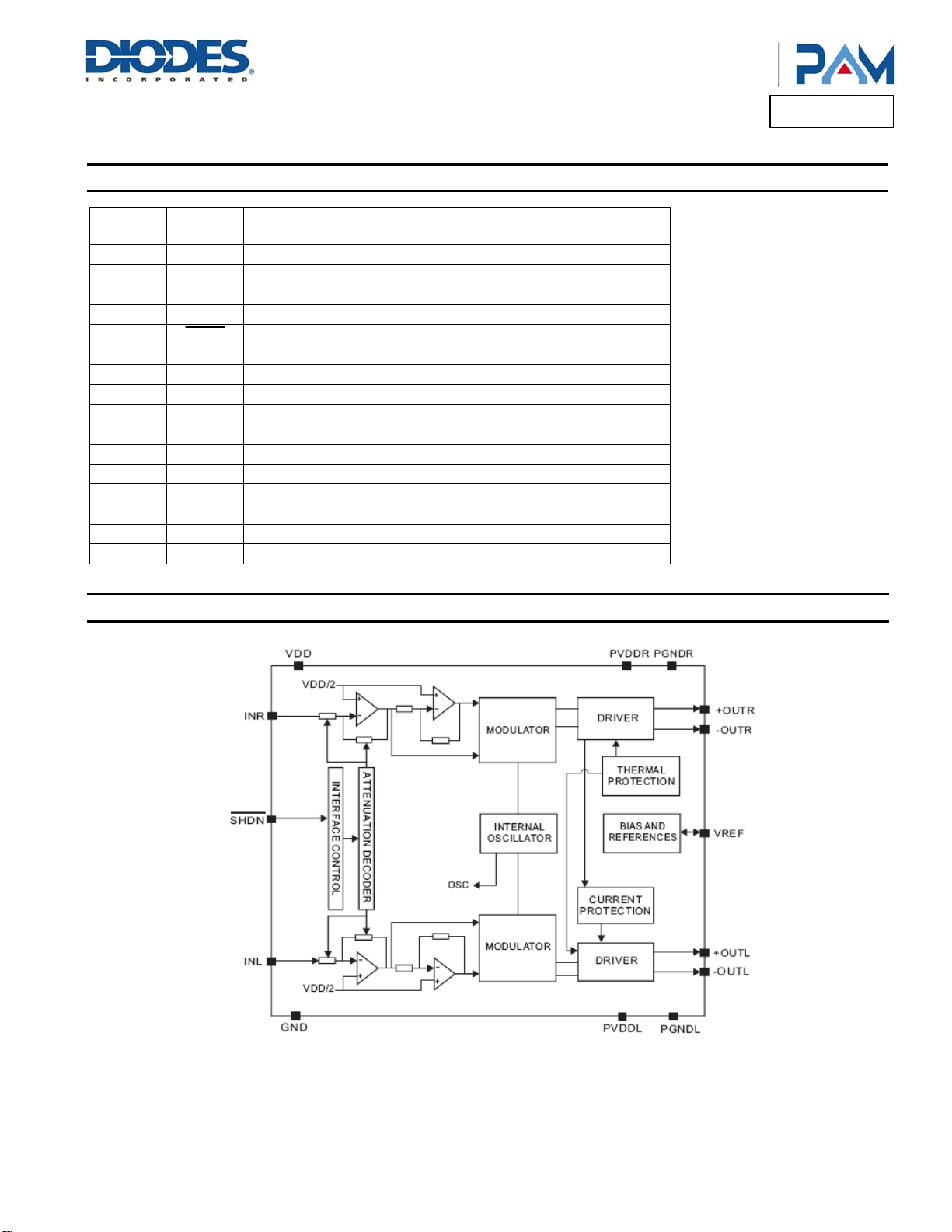
Functional Block Diagram
Product Line o
Diodes Incorporated
PAM8004
Function
PAM8004
Document number: DSxxxxx Rev. 1 - 0
2 of 11
www.diodes.com
November 2012
© Diodes Incorporated

A
f
Product Line o
Diodes Incorporated
PAM8004
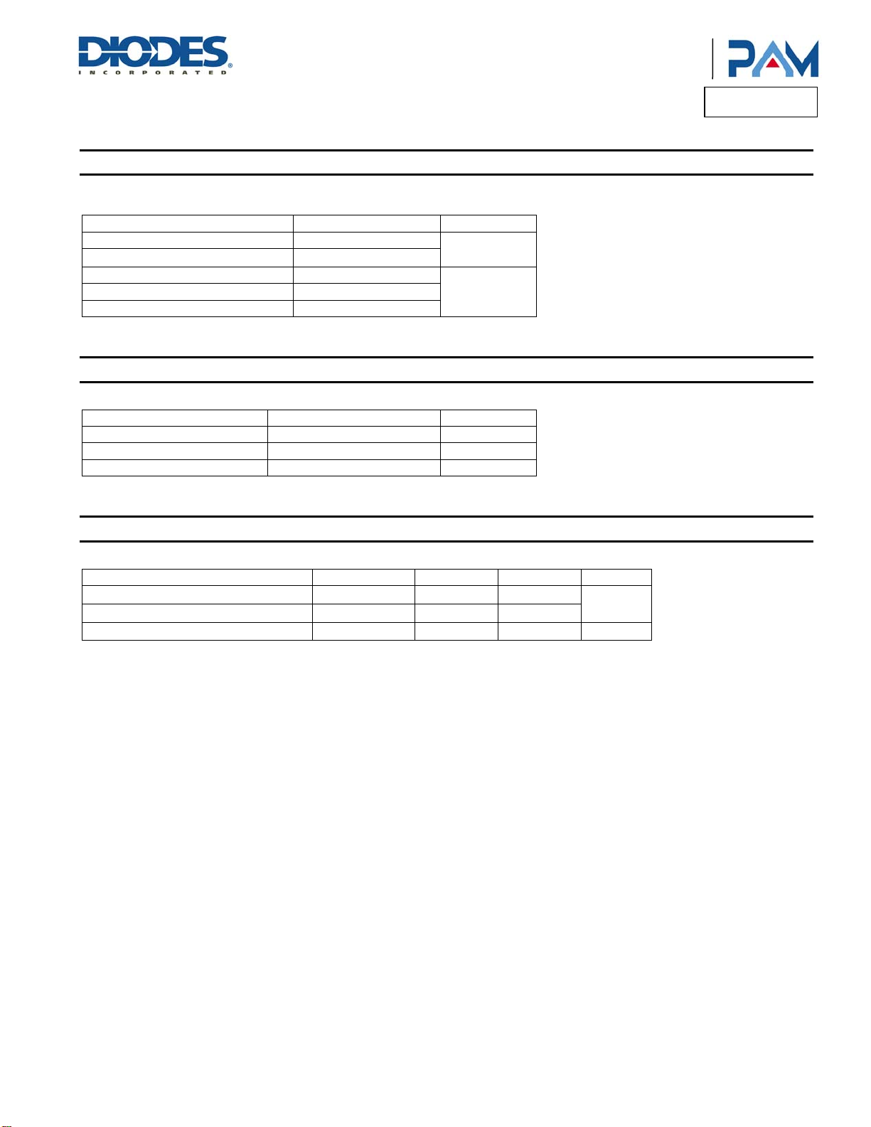
Absolute Maximum Ratings (@T
These are stress ratings only and functional operation is not implied. Exposure to absolute maximum ratings for prolonged time periods may
affect device reliability. All voltages are with respect to ground.
Parameter Rating Unit
Supply Voltage 6.0
Input Voltage
Maximum Junction Temperature 150
Storage Temperature -65 to 150
Soldering Temperature 300, 5sec
Recommended Operating Conditions (@T
Parameter Rating Unit
Supply Voltage Range 2.5 to 5.5 V
Operation Temperature Range -40 to +85 °C
Junction Temperature Range -40 to +125 °C
= +25°C, unless otherwise specified.)
A
-0.3 to V
DD
+0.3
= +25°C, unless otherwise specified.)
A
V
°C
Thermal Information
Parameter Package Symbol Max Unit
Thermal Resistance (Junction to Ambient) SOP-16L
Thermal Resistance (Junction to Case) SOP-16L
Internal Power Dissipation @ TA = +25°C
PAM8004
Document number: DSxxxxx Rev. 1 - 0
SOP-16L
www.diodes.com
JA
JC
PD
3 of 11
110
23
900 mW
°C/W
November 2012
© Diodes Incorporated

A
f
Product Line o
Diodes Incorporated
PAM8004
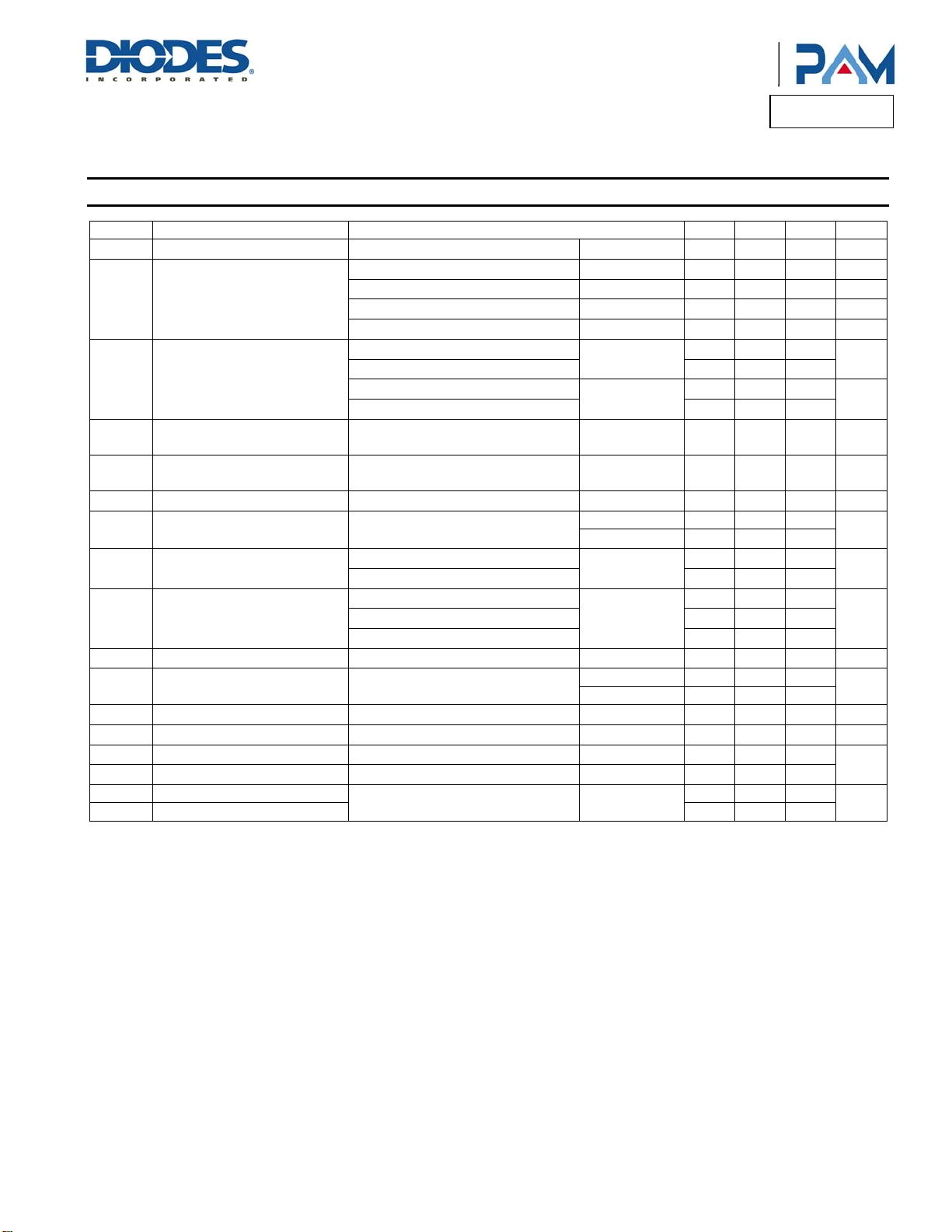
Electrical Characteristics (@T
Symbol Parameter Test Conditions Min Typ Max Units
VIN
PO
THD+N
PSRR Power Supply Ripple Rejection
CS
SNR Signal-to-Noise
VN
ISD
R
DS(ON)
fsw Switching Frequency
VOS
VIH
VIL
OTP Over Temperature Protection
OTH Over Temperature Hysterisis 30
PAM8004
Document number: DSxxxxx Rev. 1 - 0
Supply Power
Output Power
Total Harmonic Distortion Plus
Noise
Crosstalk
Output Noise
Efficiency
Quiescent Current
IQ
Shutdown Current
Static Drain-to-Source On-State
Resistor
Output Offset Voltage
Enable Input High Voltage
Enable Input Low Voltage
= +25°C, VDD = 5V, Gain = 24dB, R
A
= 8, unless otherwise specified.)
L
THD+N = 10%, f = 1kHz, R
= 4 V
L
THD+N = 1%, f = 1kHz, RL = 4 V
THD+N = 10%, f = 1kHz, RL = 8 V
THD+N = 1%, f = 1kHz, RL = 8 V
= 5.0V, Po = 0.5W, RL = 8
V
DD
V
= 3.6V, Po = 0.5W, RL = 8
DD
V
= 5.0V, Po = 1W, RL = 4
DD
V
= 3.6V, Po = 1W, RL = 4
DD
V
= 5.0V, Inputs AC-Grounded with
DD
C
= 0.47F, Gv = 6dB
IN
V
= 5V, Po = 0.5W, RL = 8,
DD
Gv = 20dB
V
= 5V, Gv = 6dB
DD
V
= 5V, Inputs AC-Grounded with
DD
= 0.47F, GV = 6dB
C
IN
R
= 8, THD = 10%
L
RL = 4, THD = 10%
= 5.0V
V
DD
V
= 3.6V
DD
V
= 3.0V
DD
V
= 2.5V to 5.5V
DD
I
= 500mA,VGS = 5V
DS
V
= 3V to 5V
DD
V
V
V
= 0V, V
IN
= 5.0V
DD
= 5.0V
DD
DD
= 5V
No Load, Junction Temperature
= 5.0V
DD
= 5.0V
DD
= 5.0V
DD
= 5.0V
DD
f = 1kHz
f = 1kHz
f = 1kHz -70 dB
f = 1kHz -93 dB
f = 1kHz 86 dB
A-weighting 33
No A-weighting 50
f = 1kHz
No load
1 µA
PMOS 0.41
NMOS 0.27
210 kHz
10 mV
1.5
0.4
V
= 5V
DD
4 of 11
www.diodes.com
2.5 5.5 V
2.5 W
2.2 W
1.65 W
1.3 W
0.16
0.12
0.17
0.26
%
%
µV
87
79
%
4.5 7.0
4.0 6.5
mA
3.7 5.5
m
V
150
November 2012
© Diodes Incorporated
°C
 Loading...