Diodes PAM8001 User Manual
f
ANTI-SATURATION FILTERLESS 2W CLASS-D STEREO AMPLIFIER
WITH DC VOLUME CONTROL AND MAX OUTPUT POWER SETTING
Description
The PAM8001 is a 2W, class-D audio amplifier. Advanced 64-step
DC volume control minimizes external components and allows
speaker volume control. PAM unique anti-saturation technology which
detects output signal clip due to the over level input signal suppress
the output signal clip automatically. Also control the gain for set max
power. It can protect low wattage speaker from overdrive damage
even same platform with high wattage model. It offers low THD+N, to
produce high-quality sound reproduction. The new filterless
architecture allows the device to drive the speaker directly, without
low-pass output filters which will save system cost and PCB area.
With the same numbers of external components, the efficiency of the
PAM8001 is much better than class-AB cousins. It can extend the
battery life thus be ideal for portable applications.
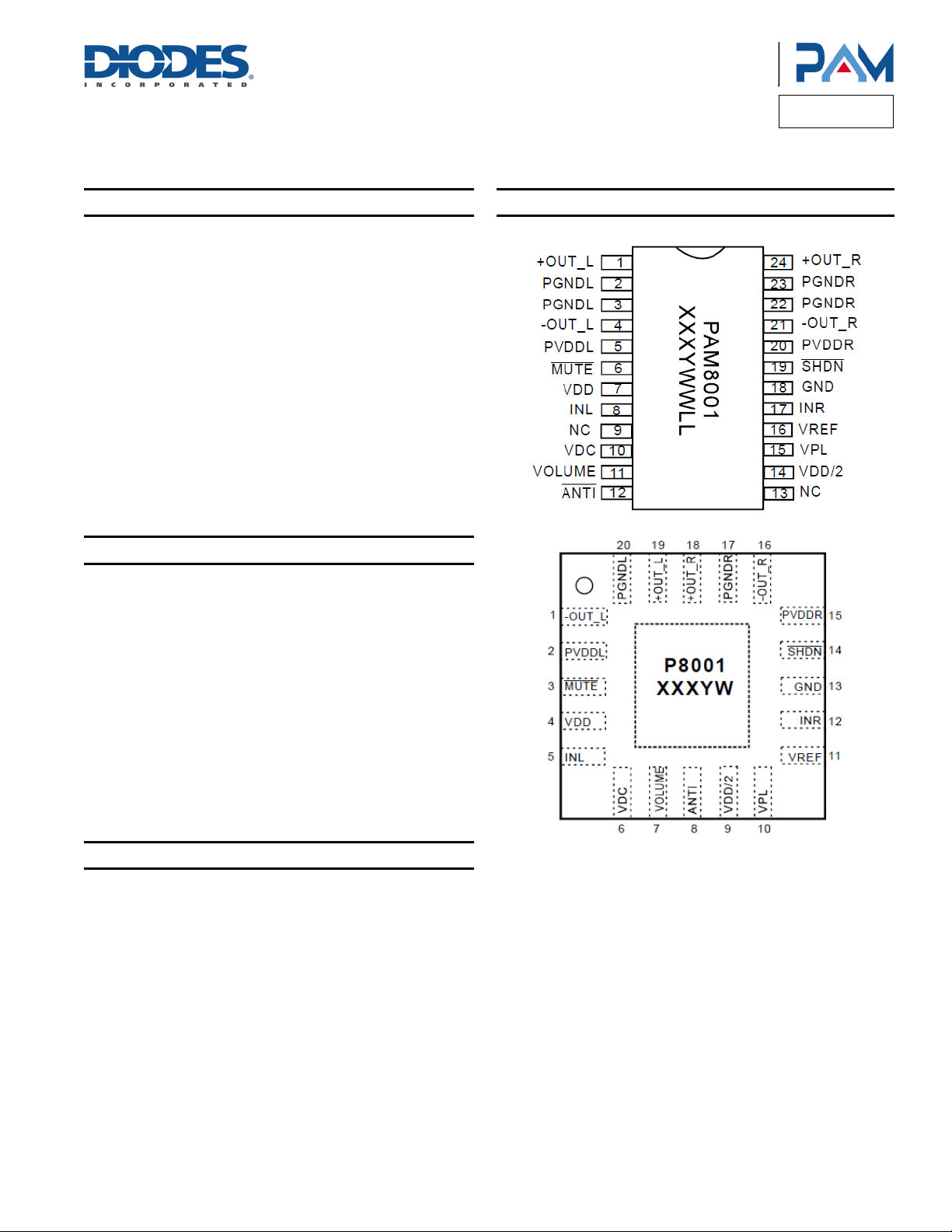
The PAM8001 is available in SSOP-24L and QFN3*3-20L package.
Features
Pin Assignments
A Product Line o
Diodes Incorporated
PAM8001
2W Output at 1% THD with a 4Ω Load at 5V Power Supply
Filterless, Low Quiescent Current and Low EMI
Low THD+N
64-Step DC Volume Control
Unique Anti-Saturation Function
Adjustable Max Output Power with No Clipping
Superior Low Noise
Low Pop Noise
Efficiency up to 90%
Short Circuit Protection
Thermal Shutdown
Few External Components to Save the Space and Cost
Pb-Free Package
Applications
LCD Monitors / TV Projectors
Notebook Computers
Portable Speakers
Portable DVD Players, Game Machines
VoIP/Speaker Phones
All In One Computer /TV
PAM8001
Document number: DSxxxxx Rev. 1 - 0
1 of 17
www.diodes.com
February 2013
© Diodes Incorporated
f
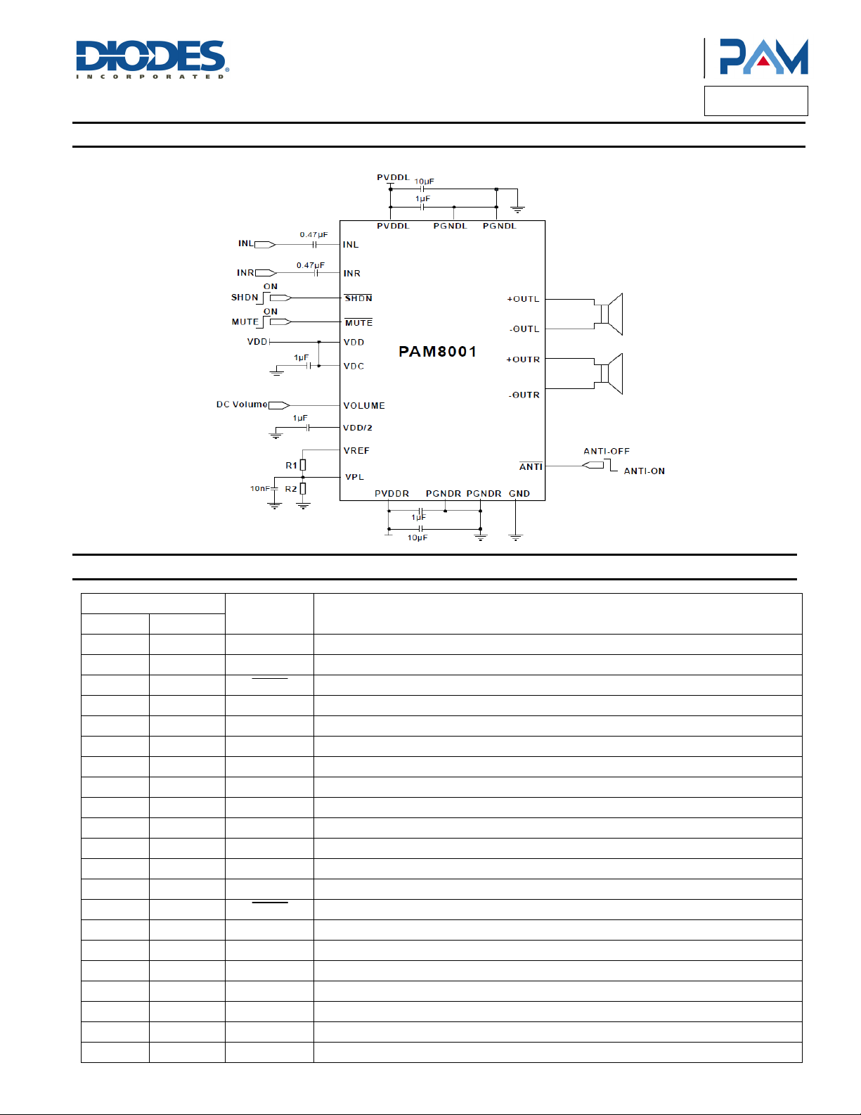
Typical Applications Circuit
A Product Line o
Diodes Incorporated
PAM8001
Pin Descriptions
Pin Number
QFN3x3 SSOP
1 4 -OUT_L Left Channel Negative Output
2 5 PVDDL Left Channel Power Supply
3 6 MUTE Mute Control Input (active low)
4 7 VDD Analog VDD
5 8 INL Left Channel Input
6 10 VDC Analog Reference for Gain Control Selection
7 11 VOLUME DC Volume Control to Set the Gain of Class-D
8 12 ANTI Anti-Saturation On/Off Control
9 14 VDD/2 Internal Common Mode Voltage, Connect a Bypass Capacitior form This Pin to GND
10 15 VPL Maximum Output Power Setting Voltage
11 16 VREF Reference Voltage Out for VPL
12 17 INR Right Channel Input
13 18 GND Analog Ground
14 19 SHDN Shutdown Control Input (active low)
15 20 PVDDR Right Channel Power Supply
16 21 -OUT_R Right Channel Negative Output
17 22/23 PGNDR Right Channel Power GND
18 24 +OUT_R Right Channel Positive Output
19 1 +OUT_L Left Channel Positive Output
20 2/3 PGNDL Left Channel Power GND
9/13 NC No Connection
PAM8001
Document number: DSxxxxx Rev. 1 - 0
Pin
Name
Function
2 of 17
www.diodes.com
February 2013
© Diodes Incorporated
f
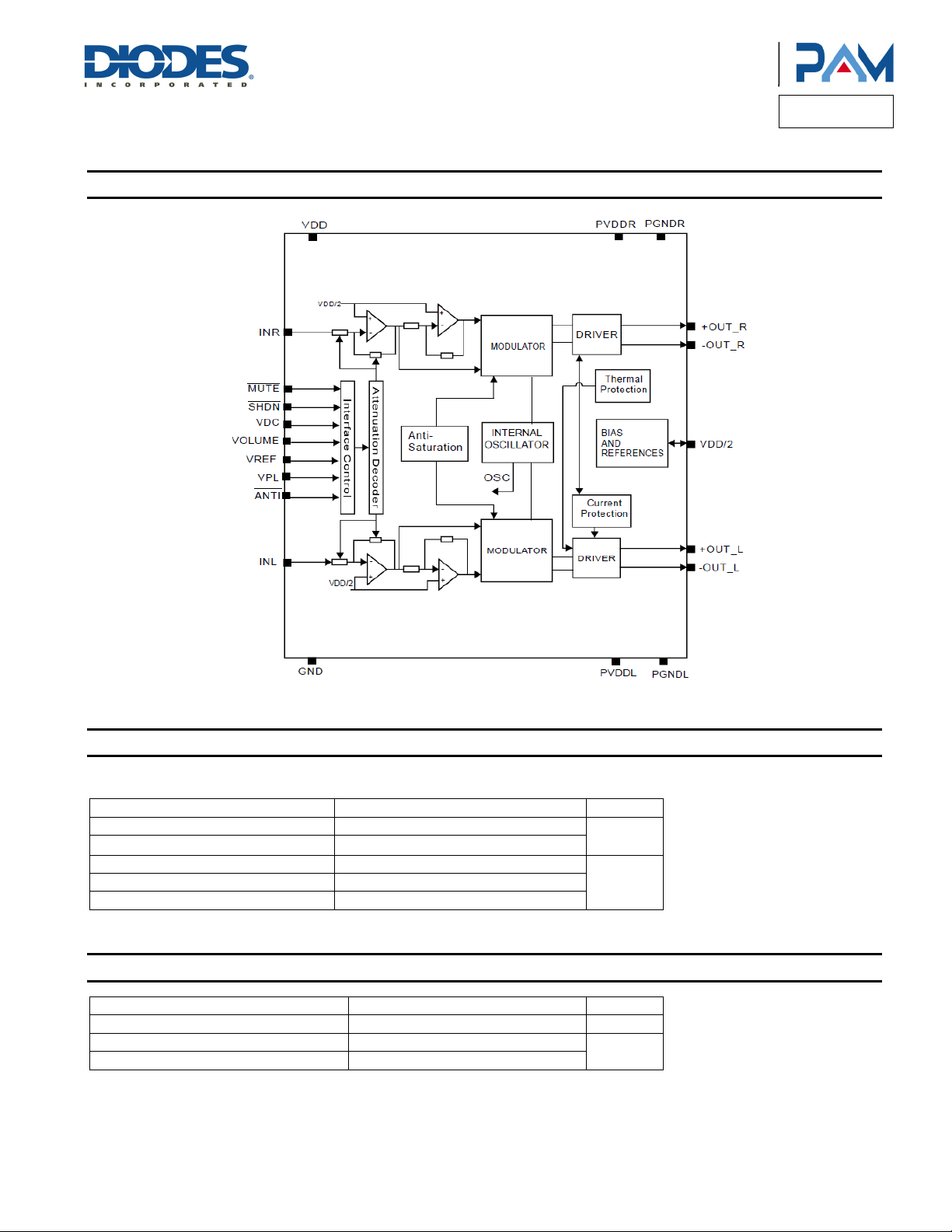
Functional Block Diagram
A Product Line o
Diodes Incorporated
PAM8001
Absolute Maximum Ratings (@T
These are stress ratings only and functional operation is not implied Exposure to absolute maximum ratings for prolonged time periods may
affect device reliability. All voltages are with respect to ground.
Parameter Rating Unit
Supply Voltage 6.0
Input Voltage
Operation Junction Temperature -40 to +125
Storage Temperature -65 to +150
Soldering Temperature 300, 5sec
Recommended Operating Conditions (@T
Parameter Rating Unit
Supply Voltage Range 2.5 to 5.5 V
Junction Temperature Range -40 to +125
Ambient Operation Temperature Range -20 to +85
PAM8001
Document number: DSxxxxx Rev. 1 - 0
= +25°C, unless otherwise specified.)
A
-0.3 to V
+0.3
DD
= +25°C, unless otherwise specified.)
A
3 of 17
www.diodes.com
V
°C
°C
February 2013
© Diodes Incorporated
f
A Product Line o
Diodes Incorporated
PAM8001
Thermal Information
Parameter Symbol Package Maximum Unit
Thermal Resistance (Junction to Ambient)
Thermal Resistance (Junction to Ambient)
θ
JA
θ
JA
Electrical Characteristics (V
= 5V, Gain = Maximum, RL = 8Ω, @TA = +25°C, unless otherwise specified.)
DD
Symbol Parameter Conditions Min Typ Max Unit
VDD
IQ
VOS
R
DS(ON)
PO
PO
THD+N
PSRR Power Supply Ripple Rejection
CS Channel Separation
f
OSC
η Efficiency
Vn Noise
SNR Signal Noise Ratio f = 20-20kHz, Gain = 6dB 85 dB
UVLO Under Voltage Lock-Out 2.0 V
I
MUTE
I
SHDN
VSH
VSL
VMH
VML
VPL V
V
REF
ID V
OTP Over Temperature Protection 150 °C
OTH Over Temperature Hysteresis 30 °C
Note: 1. Maximum Output Power vs. VPL Voltage
V
VPL (V) 0 0.1 0.2 0.3 0.4 0.5 0.6 0.7 0.8 0.9 1.0 1.1 1.2 >1.5
PO (W) 0 0.04 0.11 0.21 0.34 0.50 0.68 0.94 1.28 1.52 1.90 2.15 2.40 2.8
Supply Voltage Range 2.5 5.5 V
Quiescent Current No Load 11.5 15 mA
Output Offset Voltage
Drain-Source On-State
Resistance
Output Power with AntiSaturation
Output Power without AntiSaturation
Total Harmonic Distortion Plus
Noise
VIN = 0V
IDS = 0.5A
THD+N <1%
f = 1kHz, V
THD+N <10%
f = 1kHz, V
=8Ω, PO = 0.85W, f = 1kHz
R
L
RL = 4Ω, PO = 1.75W, f = 1kHz
Input AC-GND, f = 1KHz,
V
= 200mV, Gain = 6dB
PP
P
= 1W, f = 1KHz
O
Oscillator Frequency 200 250 300 kHz
P
= 1.7W, f = 1KHz, RL = 8Ω
O
PO = 3.0W, f = 1KHz, RL = 4Ω
Input AC-GND
Gain = 6dB
Mute Current
Shutdown Current
V
V
MUTE
SHDN
SHDN Input High 1.3
SHDN Input Low 0.65
MUTE Input High 1.3
MUTE Input Low 0.66
Threshold Voltage
PL
V
DD
Voltage VDD = 2.5V to 5.5V
REF
Drive Current VDD = 2.5V to 5.5V
REF
= 5V, RL = 4Ω, TA = +25°C
Power Limit Off 1.5 Note 1 V
SSOP-24L 96 °C/W
QFN3*3-20L 31 °C/W
20 mV
= 1V
PL
= 1.5V
PL
P MOSFET 0.21
N MOSFET 0.165
=8Ω
R
L
RL = 4Ω
=8Ω
R
L
RL = 4Ω
1
1.9
1.35 1.5
2.65 2.8
0.08
0.08
Ω
W
W
%
70 dB
-85 dB
85 89 %
80 83 %
= 0.3V
= 0V
A-Weighting 50
No A-Weighting 70
4.2 mA
1 µA
µV
V
V
1.2 V
150 µA
PAM8001
Document number: DSxxxxx Rev. 1 - 0
4 of 17
www.diodes.com
February 2013
© Diodes Incorporated
f
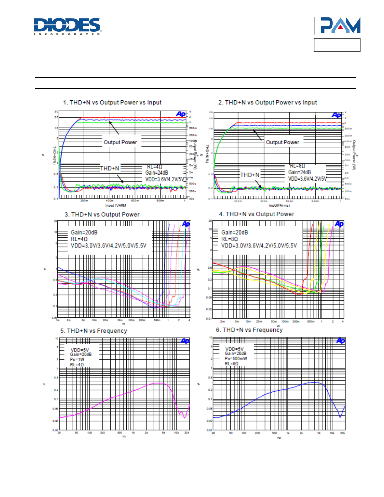
Typical Operating Characteristics (@T
= +25°C, unless otherwise specified.)
A
A Product Line o
Diodes Incorporated
PAM8001
PAM8001
Document number: DSxxxxx Rev. 1 - 0
5 of 17
www.diodes.com
February 2013
© Diodes Incorporated
f
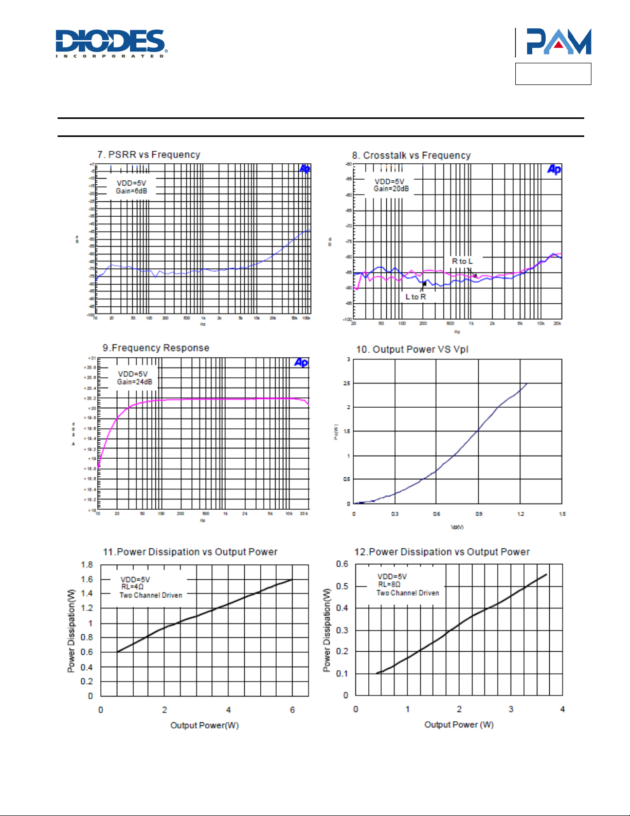
Typical Operating Characteristics (cont.) (@T
A Product Line o
Diodes Incorporated
= +25°C, unless otherwise specified.)
A
PAM8001
PAM8001
Document number: DSxxxxx Rev. 1 - 0
6 of 17
www.diodes.com
February 2013
© Diodes Incorporated
 Loading...