

Denon DRA-697CIE Service Manual
For U.S.A. & Canada model
SERVICE MANUAL
Ver. 1
MODEL
AM-FM STEREO RECEIVER
DRA-697CI
注 意
サービスをおこなう前に、このサービスマニュアルを
必ずお読みください。本機は、火災、感電、けがなど
に対する安全性を確保するために、さまざまな配慮を
おこなっており、また法的には「電気用品安全法」に
もとづき、所定の許可を得て製造されております。
従ってサービスをおこなう際は、これらの安全性が維
持されるよう、このサービスマニュアルに記載されて
いる注意事項を必ずお守りください。
●
For purposes of improvement, specifications and
design are subject to change without notice.
●
Please use this service manual with referring to the
operating instructions without fail.
●
Some illustrations using in this service manual are
slightly different from the actual set.
Denon Brand Company, D&M Holdings Inc.
●
●
●
●
TOKYO, JAPAN
本機の仕様は性能改良のため、予告なく変更すること
があります。
補修用性能部品の保有期間は、製造打切後8年です。
修理の際は、必ず取扱説明書を参照の上、作業を行っ
てください。
本文中に使用しているイラストは、説明の都合上現物
と多少異なる場合があります。
X0315V.01 DE/CDM 0609
SAFETY PRECAUTIONS
The following check should be performed for the continued protection of the customer and service technician.
LEAKAGE CURRENT CHECK
Before returning the unit to the customer, make sure you make either (1) a leakage current check or (2) a line to chassis
resistance check. If the leakage current exceeds 0.5 milliamps, or if the resistance from chassis to either side of the power
cord is less than 460 kohms, the unit is defective.
DRA-697CI
CAUTION
Please heed the points listed below during servicing and inspection.
◎ Heed the cautions!
Spots requiring particular attention when servicing, such as
the cabinet, parts, chassis, etc., have cautions indicated on
labels or seals. Be sure to heed these cautions and the cautions indicated in the handling instructions.
◎ Caution concerning electric shock!
(1) An AC voltage is impressed on this set, so touching inter-
nal metal parts when the set is energized could cause
electric shock. Take care to avoid electric shock, by for example using an isolating transformer and gloves when
servicing while the set is energized, unplugging the power
cord when replacing parts, etc.
(2)There are high voltage parts inside. Handle with extra care
when the set is energized.
◎
Caution concerning disassembly and assembly!
Though great care is taken when manufacturing parts from
sheet metal, there may in some rare cases be burrs on the
edges of parts which could cause injury if fingers are moved
across them. Use gloves to protect your hands.
◎ Only use designated parts!
The set's parts have specific safety properties (fire resistance, voltage resistance, etc.). For replacement parts, be
sure to use parts which have the same properties. In particular, for the important safety parts that are marked ! on wiring
diagrams and parts lists, be sure to use the designated parts.
◎ Be sure to mount parts and arrange the
wires as they were originally!
For safety reasons, some parts use tape, tubes or other insulating materials, and some parts are mounted away from the
surface of printed circuit boards. Care is also taken with the
positions of the wires inside and clamps are used to keep
wires away from heating and high voltage parts, so be sure to
set everything back as it was originally.
◎ Inspect for safety after servicing!
Check that all screws, parts and wires removed or disconnected for servicing have been put back in their original positions, inspect that no parts around the area that has been
serviced have been negatively affected, conduct an insulation
check on the external metal connectors and between the
blades of the power plug, and otherwise check that safety is
ensured.
(Insulation check procedure)
Unplug the power cord from the power outlet, disconnect the
antenna, plugs, etc., and turn the power switch on. Using a
500V insulation resistance tester, check that the insulation resistance between the terminals of the power plug and the externally exposed metal parts (antenna terminal, headphones
terminal, microphone terminal, input terminal, etc.) is 1MΩ or
greater. If it is less, the set must be inspected and repaired.
CAUTION
Many of the electric and structural parts used in the set have
special safety properties. In most cases these properties are
difficult to distinguish by sight, and using replacement parts
with higher ratings (rated power and withstand voltage) does
not necessarily guarantee that safety performance will be preserved. Parts with safety properties are indicated as shown
below on the wiring diagrams and parts lists is this service
manual. Be sure to replace them with parts with the designated part number.
(1) Schematic diagrams ... Indicated by the ! mark.
(2) Parts lists ... Indicated by the ! mark.
Concerning important safety parts
Using parts other than the designated parts
could result in electric shock, fires or other
dangerous situations.
注 意
サービス、点検時にはつぎのことにご注意願います。
◎注意事項をお守りください!
サービスのとき特に注意を必要とする個所についてはキャ
ビネット、部品、シャーシなどにラベルや捺印で注意事項を
表示しています。これらの注意書きおよび取扱説明書などの
注意事項を必ずお守りください。
◎感電に注意!
(1) このセットは、交流電圧が印加されていますので通電時
に内部金属部に触れると感電することがあります。従っ
て通電サービス時には、絶縁トランスの使用や手袋の着
用、部品交換には、電源プラグを抜くなどして感電にご
注意ください。
(2) 内部には高電圧の部分がありますので、通電時の取扱に
は十分ご注意ください。
◎分解、組み立て作業時のご注意!
板金部品の端面の『バリ』は、部品製造時に充分管理をして
おりますが、板金端面は鋭利となっている箇所が有りますの
で、部品端面に触れたまま指を動かすとまれに怪我をする場
合がありますので十分注意して作業して下さい。手の保護の
ために手袋を着用してください。
◎指定部品の使用!
セットの部品は難燃性や耐電圧など安全上の特性を持った
ものとなっています。従って交換部品は、使用されていたも
のと同じ特性の部品を使用してください。特に配線図、部品
表に!印で指定されている安全上重要な部品は必ず指定の
ものをご使用ください。
◎部品の取付けや配線の引きまわしは、
元どおりに!
安全上、テープやチューブなどの絶縁材料を使用したり、プ
リント基板から浮かして取付けた部品があります。また内部
配線は引きまわしやクランパーによって発熱部品や高圧部
品に接近しないように配慮されていますので、これらは必ず
元どおりにしてください。
◎サービス後は安全点検を!
サービスのために取り外したねじ、部品、配線などが元どお
りになっているか、またサービスした個所の周辺を劣化させ
てしまったところがないかなどを点検し、外部金属端子部
と、電源プラグの刃の間の絶縁チェックをおこなうなど、安
全性が確保されていることを確認してください。
(絶縁チェックの方法)
電源コンセントから電源プラグを抜き、アンテナやプラグな
どを外し、電源スイッチを入れます。500V 絶縁抵抗計を用
いて、電源プラグのそれぞれの端子と外部露出金属部[アン
テナ端子、ヘッドホン端子マイク端子、入力端子など]との
間で、絶縁抵抗値が1 MΩ 以上であること、この値以下の
ときはセットの点検修理が必要です。
注 意
本機に使用している多くの電気部品、および機構部品は安全
上、特別な特性を持っています。この特性はほとんどの場合、
外観では判別つきにくく、またもとの部品より高い定格(定
格電力、耐圧)を持ったものを使用しても安全性が維持され
るとは、限りません。安全上の特性を持った部品は、この
サービスマニュアルの配線図、部品表につぎのように表示し
ていますので必ず指定されている部品番号のものを使用願
います。
(1) 配線図…
(2) 部品表…
安全上重要な部品について
!マークで表示しています。
!マークで表示しています。
指定された部品と異なるものを使用した場合に
は、感電、火災などの危険を生じる恐れがあり
ます。
2
DRA-697CI
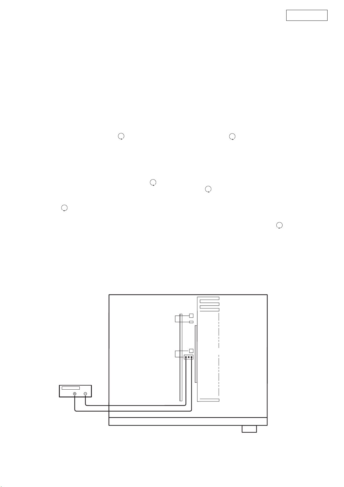
ADJUSTMENT
Idling Current
Required measurement equipment: DC Voltmeter
1. Preparation
(1) Avoid direct blow from an air conditioner or an electric
fan, and adjust the unit at normal room temperature 15 °C
~ 30 °C (59 °F ~ 86 °F).
(2) Presetting
• POWER (Power source switch) OFF
• SPEAKER (Speaker terminal) No load
(Do not connect speaker, dummy resistor, etc.)
2. Adjustment
(1) Remove top cover and set VR501FL, VR501FR on MAIN
Unit at fully counterclockwise ( ) position.
(2) Connect DC Voltmeter to test points (FRONT-Lch:
TP501, FRONT-Rch: TP502).
(3) Connect power cord to AC Line, and turn power switch
"ON".
(4) Presetting.
MASTER VOLUME : "---" counterclockwise ( min.)
MODE : TONE DEFEAT
FUNCTION : CD
(5) Within 2 minutes after the power on, turn VR501FL clock-
wise ( ) to adjust the TEST POINT voltage to 1.5 mV
± 0.5 mV DC.
(6) After 10 minutes from the preset above, turn VR501FL to
set the voltage to 2.0 mV ± 0.5 mV DC.
(7) Adjust the Variable Resistors of other channels in the
same way.
調整
アイドリング電流の調整
調整に必要な測定器 : DCVoltmeter
1. 準備
(1) セットをクーラ、扇風機のそばなど風通しの良い場所
を避け、通常の使用状態に置きます。セットの周囲温
度は 15〜30 ℃、湿度は常湿とします。
(2) プリセット
・電源スイッチ OFF
・スピーカ端子 無負荷
( スピーカ・ダミー抵抗器などを接続しない。)
2. 調整
(1) 上カバーをはずし、メイン基板の VR501FL,VR501FR を
反時計方向 ( )に回し切った状態にセットします。
(2) テストポイント (FRONT-Lch:TP501,FRONT-Rch:
に DCVoltmeterを接続します。
(3) 電源コードを AC100V(95〜105Vの範囲でも可)に接
続し、電源スイッチを "ON"にします。
(4) ON後、次のようにセットします。
・MASTERVOLUME(音量調節つまみ)→反時計方向
( )に回す、最小の状態にする。
・SPEAKER(スピーカ端子)→無負荷(スピーカ、
ダミー抵抗器などを接続しない。)
MODE :TONEDEFEAT
FUNCTION :CD
(5) 2分以内に VR501FLを時計方向 ( ) に回しテストポ
イントの電圧を次のように調整します。
1.5mV ±0.5mVDC
(6) 予備調整から 10分後 VR501FLを回し、次のように電圧
を設定します。
2.0mV± 0.5mVDC
(7) 同じ方法で各チャネルの可変抵抗を調整します。
TP502)
DC Voltmeter
FLch
FRch
VR501FL
TP501
VR501FR
TP502
3
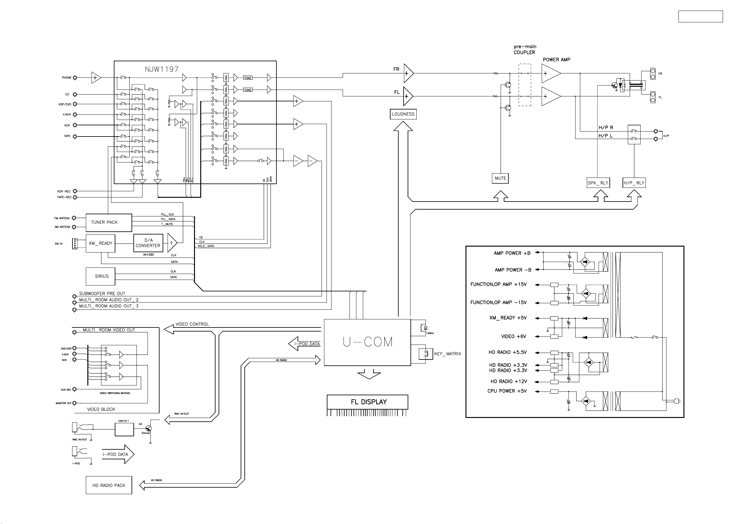
BLOCK DIAGRAM
DRA-697CI
4
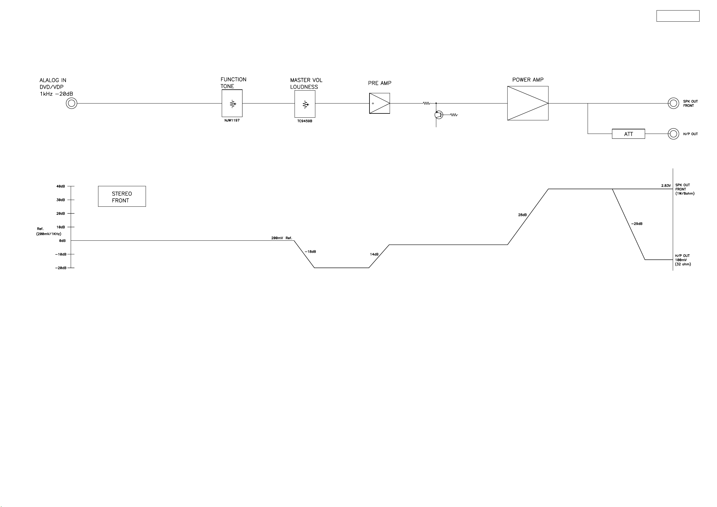
LEVEL DIAGRAM
DRA-697CI
5
SEMICONDUCTORS
Only major semiconductors are shown, general semiconductors etc. are omitted to list.
主な半導体を記載しています。汎用の半導体は記載を省略しています。
1. IC’s
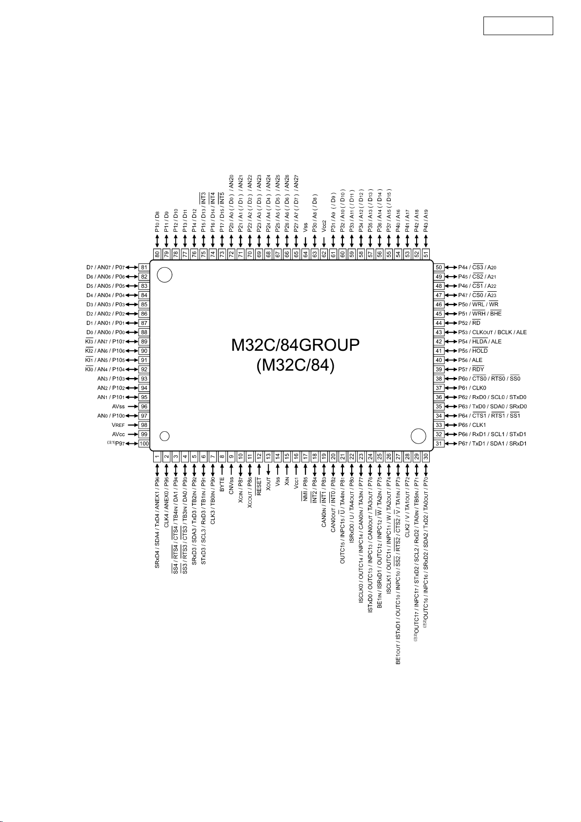
M30843FHFP (IC401) FRONT P.W.B.
DRA-697CI
6
M30843FHFP Terminal Function
DRA-697CI
PIN No. Port Function Port Name
1P96, T
XD4/SDA4/SRXD4 SIRIUS_TX O O/L SIRIUS data transmission
P-ON
I/O
Standby
Function
2 P95, CLK4 SIRIUS MUTE O O/L SIRIUS MUTE control
3 P94 (HD CE) O O/L HD Radio enable output
4 P93 MULT3 SW O O/L ZONE3 output, HPFcontrol
5P92, T
6P91, T
XD3/SDA3/SRXD3 HD Radio TX/(SDA) O O/L HD Radio data transmission
XD3/SDA3/SRXD3 HD Radio RX/(SCL) I I HD Radio Data reception
7 P90, CLK3 (HD CLK) O O/L HD Radio clock output
8 BYTE I - Ext. data bus bit width switching
9 CNV
10 P87, X
11 P8 6 , X
SS I - Processor mode switching
CIN (HD RESET) O O/L HD Radio reset output
COUT FLT_RESET O O/L FLT reset output
12 /RESET I - Hard reset
13 X
14 V
15 X
16 V
OUT O - Oscillator connection
SS I-GND
IN I - Oscillator connection
CC1 I-5V
17 P85 NMI I - NMI interruption input
18 P84, /INT2 RS232C_T
X I I RS232C signal detection
19 P83, /INT1 REMOCON I I Remote control input
20 P82, /INT0 PROTECTION I I Unusual operation detection
21 P81 FLT_CLK O O/L FLT clock output
22 P80 FLT_DATA O O/L FLT data output
23 P77 FLT_CE1 O O/L FLT chip select output
24 P76 SPK_RLY_A O O/L Speaker A Relay control
25 P75 CPU_5V_SW O O/L CPU 5V control
26 P74 SPK_RLY_B O O/L Speaker B Relay control
27 P73 (NC) O/L
28 P72, CLK2 iPod_DET I I iPod connection detection
29 P71, R
30 P70, T
31 P67, T
32 P66, R
XD2/SCL2/STXD2 iPod_RX I I iPod data reception
XD2/SDA2/SRXD2 iPod_TX O O/L iPod data transmission
XD1/SDA1/SRXD1 RS232C_TX O O/L RS232C data reception
XD1/SCL1/STXD1 RS232C_RX I I RS232C data reception
33 P65, CLK1 PLL_DI I I PLL data input
34 P64 PLL_DO/XM-DAC_DO O O/L PLL/XM-DAC data output
35 P63, T
36 P62, R
XD0/SDA0/SRXD0 XM_TX O O/L XM data transmission
XD0/SCL0/STXD0 XM_RX I I XM data reception
37 P61, CLK0 PLL_CLK/XM-DAC_CLK O O/L PLL/XM-DAC clock output
38 P60 PLL_CE O O/L PLL enable output
39 P57 /TUNED I I TUNED detection
40 P56 /STEREO I I STEREO broadcast detection
41 P55 RS232C_UPDATE_EPM
42 P54 VOL_UP I I Volume encoder input
43 P53 VOL_DOWN I I Volume encoder input
44 P52 SELECT_DOWN I I Select encoder input
45 P51 SELECT_UP I I Select encoder input
46 P50 RS232C_UPDATE_CE O O/L
47 P47 DC TRIGGER_2ON O O/L Trigger Out2 ON/OFF control
48 P46 FUNCTION_UP I I Function encoder input
49 P45 TUNER MUTE O O/L TUNER MUTE control
50 P44 E2PROM_SCL O O/L E2P Clock output
51 P43 E2PROM_SDA I/O O/L E2PROM data transmission and reception
52 P42 ZONE3_MUTE O O/L ZONE3 MUTE control
53 P41 ZONE2_MUTE O O/L ZONE2 MUTE control
54 P40 STBY LED_RED O O/L StandbyLED(R) control
7
DRA-697CI
PIN No. Port Function Port Name
P-ON
I/O
Standby
Function
55 P37 HD Radio MUTE O O/L HD Radio MUTE control
56 P36 DC TRIGGER 1 O O/L Trigger Out1 ON/OFF control
57 P35 H/P RELAY O O/L H/P Relay control
58 P34 SW_MUTE O O/L SW MUTE control
59 P33 VIDEO OFF O O/L VIDEO Reg control
60 P32 HD Radio DET I I HD Radio Installing detection
61 P31 HD Radio P/E O O/L HD Radio power supply control
62 V
CC2 I-5V
63 P30 (NC)
64 V
SS I-GND
65 P27 XM_DBPOWER O O/L XM Reg control
66 P26 XM_DIC_RESET O O/L XM DIC reset output
67 P25 XM_DAC_PDN O O/L XM DAC reset reset output
68 P24 XM_COMMAND O O/L XM DIC CBM output
69 P23 XM_REQ I I XM DIC Interrupt request
70 P22 H/P DET I I H/P connection detection
71 P21 POWER RELAY O O/L POWER RELAY control
72 P20 FUNCTION_DOWN I I Function encoder input
73 P17, /INT5 POWER DOWN I I CPU 5.6V detection
74 P16, /INT4 ETHERNET REQ I I ETHERNET interrupt request
75 P15, /INT3 POWER I I POWER Key input detection
76 P14 MULT2 SW O O/L ZONE3 output §HPF control
77 P13 STBY_LED_GREEN O O/L Standby LED(G) control
78 P12 NJW1197W_LATCH O O/L NJW1197 latch output
79 P11 NJW1197W_CLK O O/L NJW1197 Clock output
80 P10 NJW1197W_DATA O O/L NJW1197 data output
81 P07 MAIN_MUTE O O/L MAIN MUTE control
82 P06 VIDEO_A O O/L VIDEO output control
83 P05 VIDEO_B O O/L VIDEO output control
84 P04 VIDEO_C O O/L VIDEO output control
85 P03 VIDEO_D O O/L VIDEO output control
86 P02 VIDEO_E O O/L VIDEO output control
87 P01 ZONE2_VIDEO_MUTE O O/L ZONE2 VIDEO MUTE control
88 P00 ZONE3_VIDEO_MUTE O O/L ZONE3 VIDEO MUTE control
89 P107 EMODE I I
90 P106, AN6 KEY_IN1 I I Key input
91 P105, AN5 KEY_IN2 I I Key input
92 P104, AN4 KEY_IN3 I I Key input
93 P103 LOUDNESS ON O O/L LOUDNESS ON/OFF control
94 P102 SIRIUS P/E O O/L SIRIUS enable output
95 P101 XM MUTE O O/L XM MUTE control
96 AV
SS I-GND
97 P100 XM_DACNS O O/L XM DAC chip select input
98 V
99 AV
100 P97, R
REF I - standard voltage input
CC I-5V
XD4/SCL4/STXD4 SIRIUS_RX I I SIRIUS data reception
8
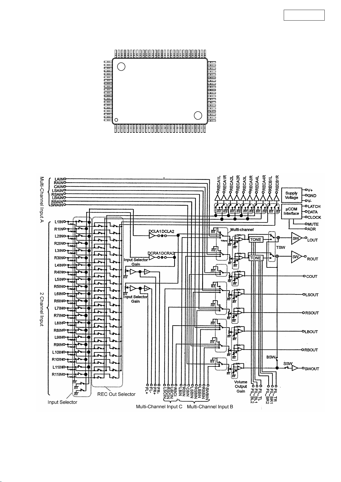
NJW1197 (IC101) INPUT P.W.B.
DRA-697CI
PIN FUNCTION
BLOCK DIAGRAM
81
100
80
51
50
31
1
30
9
DRA-697CI
NJW1197 Terminal Function
No. SYMBOL FUNCTION No. SYMBOL FUNCTION
1 ROUT Rch output 51 DCR_IN Multi-channel selector Rch input
2 COUT Cch output 52 DCR_OUT Input selector Rch output
3 LSOUT LSch output 53 GND Ground
4 RSOUT RSch output 54 DCL_IN Multi-channel selector Lch input
5 LBOUT LBch output 55 DCL_OUT Input selector Lch output
6 RBOUT RBch output 56 GND Ground
7 SWOUT SWch output 57 REC_B1R Input selector Rch REC output B1
8 GND Ground 58 REC_B1L Input selector Lch REC output B1
9 FIL_BL2 Lch Bass filter terminal 2 59 REC_A4R Input selector Rch REC output A4
10 FIL_BL1 Lch Bass filter terminal 1 60 REC_A4L Input selector Lch REC output A4
11 FIL_TL Lch Treble filter terminal 61 REC_A3R Input selector Rch REC output A3
12 TCAP Switching noise rejection capacitor 62 REC_A3L Input selector Lch REC output A3
13 FIL_BR2 Rch Bass filter terminal 2 63 REC_A2R Input selector Rch REC output A2
14 FIL_BR1 Rch Bass filter terminal 1 64 REC_A2L Input selector Lch REC output A2
15 FIL_TR Rch Treble filter terminal 65 REC_A1R Input selector Rch REC output A1
16 V+ + Power supply voltage input 66 REC_A1L Input selector Lch REC output A1
17 ADR Chip address select input 67 VDDOUT Internal Digital +Power Supply Output
18 V- - Power supply voltage input 68 DATA Control data signal input
19 L1IN Input selector Lch input 1 69 CLOCK Clock signal input
20 DCCAP_SW Switching noise rejection capacitor 70 LATCH Latch signal input
21 R1IN Input selector Rch input 1 71 MUTE External Mute control
22 DCCAP_RB Switching noise rejection capacitor 72 FL+ Input selector gain control Lch no-inverted output
23 L2IN Input selector Lch input 2 73 FL- Input selector gain control Lch inverted output
24 DCCAP_LB Switching noise rejection capacitor 74 FR+ Input selector gain control Rch no-inverted output
25 R2IN Input selector Rch input 2 75 FR- Input selector gain control Rch inverted output
26 DCCAP_RS Switching noise rejection capacitor 76 GND Ground
27 L3IN Input selector Lch input 3 77 LSCIN Multi-channel LSch input C
28 DCCAP_LS Switching noise rejection capacitor 78 RSCIN Multi-channel RSch input C
29 R3IN Input selector Rch input 3 79 LBCIN Multi-channel LBch input C
30 DCCAP_C Switching noise rejection capacitor 80 RBCIN Multi-channel RBch input C
31 L4IN Input selector Lch input 4 81 GND Ground
32 DCCAP_R Switching noise rejection capacitor 82 LAIN Multi-channel Lch input A
33 R4IN Input selector Rch input 4 83 RAIN Multi-channel Rch input A
34 DCCAP_L Switching noise rejection capacitor 84 CAIN Multi-channel Cch input A
35 L5IN Input selector Lch input 5 85 LSAIN Multi-channel LSch input A
36 GND Ground 86 RSAIN Multi-channel RSch input A
37 R5IN Input selector Rch input 5 87 LBAIN Multi-channel LBch input A
38 GND Ground 88 RBAIN Multi-channel RBch input A
39 L6IN Input selector Lch input 6 89 SWAIN Multi-channel SWch input A
40 L9IN Input selector Lch input 9 90 GND Ground
41 R6IN Input selector Rch input 6 91 LBIN Multi-channel Lch input B
42 R9IN Input selector Rch input 9 92 RBIN Multi-channel Rch input B
43 L7IN Input selector Lch input 7 93 CBIN Multi-channel Cch input B
44 L10IN Input selector Lch input 10 94 LSBIN Multi-channel LSch input B
45 R7IN Input selector Rch input 7 95 RSBIN Multi-channel RSch input B
46 R10IN Input selector Rch input 10 96 LBBIN Multi-channel LBch input B
47 L8IN Input selector Lch input 8 97 RBBIN Multi-channel RBch input B
48 L11IN Input selector Lch input 11 98 SWBIN Multi-channel SWch input B
49 R8IN Input selector Rch input 8 99 GND Ground
50 R11IN Input selector Rch input 11 100 LOUT Lch output
10
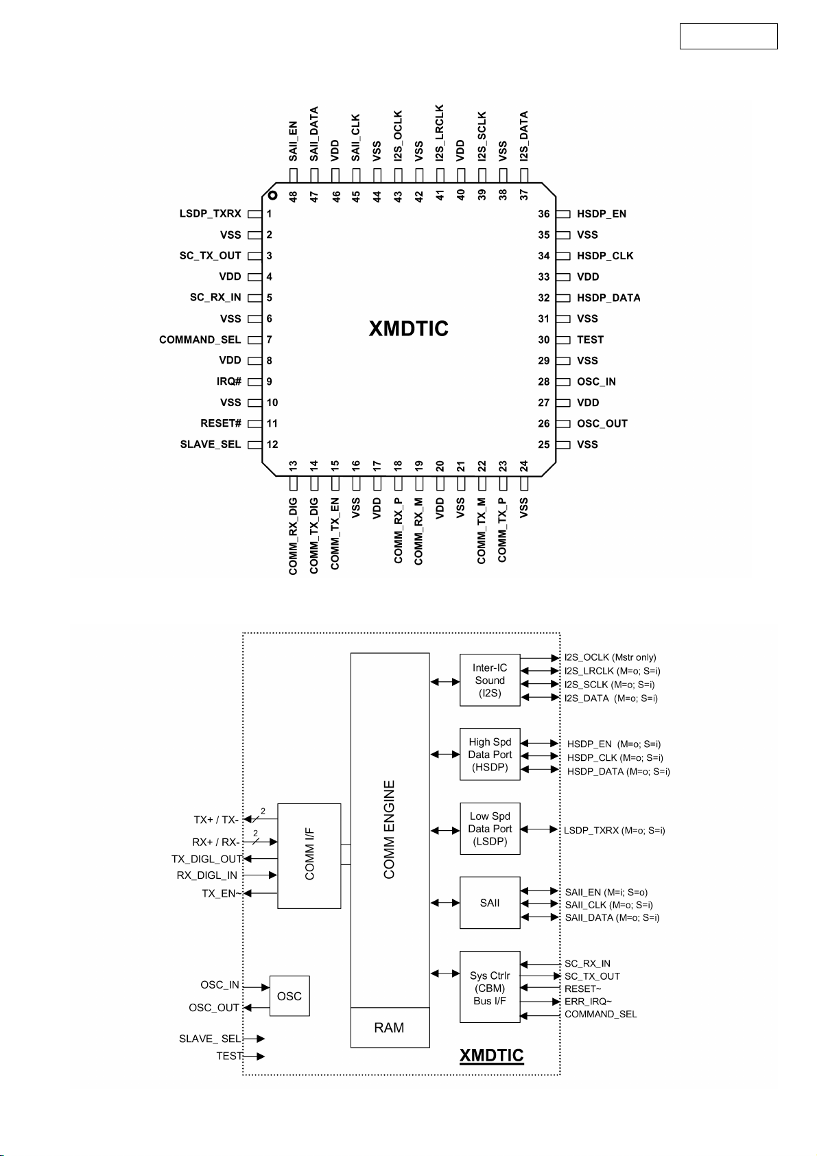
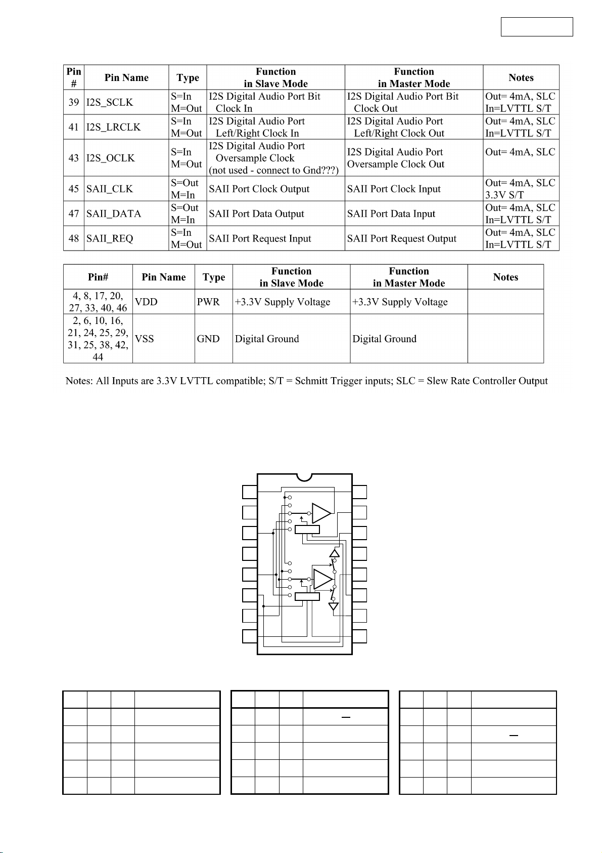
F2602-1 XMDTIC (IC203) XM-READY P.W.B.
DRA-697CI
Functional Description
11
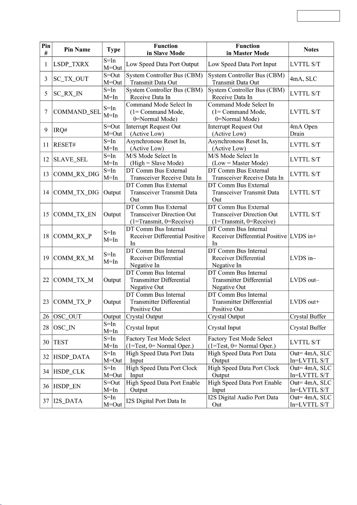
F2602-1 XMDTIC Pin Descriptions
DRA-697CI
12
DRA-697CI
BA7626F (IC601) MAIN P.W.B.
Block diagram
Monitor OUT
Truth table
ABE
LL
HL
LH
∗
∗
∗
H H L IN4
HHH IN5
Note 1:∗indicates "don't care" (H or L).
Monitor OUT
IN1
IN2
IN3
1
GND
IN5
GND
IN4
CTL E
IN3
CTL D
2
3
4
5
6
7
8
6dB
logic
6dB
logic
CDE VOUT1
LL
HL
LH
∗
∗
∗
HHL IN4
H H H IN5
IN2
IN3
16
IN1
CTL A
15
CC
V
14
13
V
CC
12
IN2
11
CTL B
10
OUT2
V
CTL C
9
CDE VOUT2
LL
HL
LH
∗
∗
∗
IN1
IN3
HHL IN4
HHH IN5
13
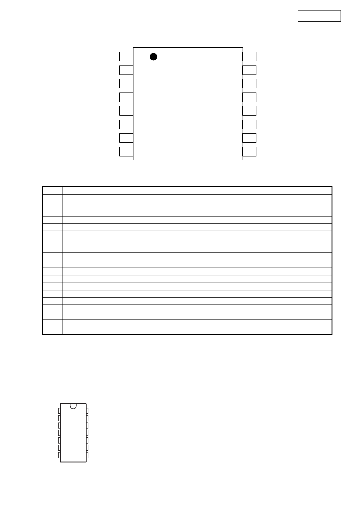
AK4385 (IC 207) XM-READY P.W.B.
DRA-697CI
MCLK
BICK
SDTI
LRCK
1
2
3
4
Top
View
PDN
CSN
CCLK
CDTI
5
6
7
8
Pin function
No. Pin Name I/O Function
1 MCLK I Master Clock Input Pin
An external TTL clock should be input on this pin.
2 BICK I Audio Serial Data Clock Pin
3 SDTI I Audio Serial Data Input Pin
4 LRCK I L/R Clock Pin
5 PDN I Power-Down Mode Pin
When at “L”, the AK4385 is in the power-down mode and is held in reset.
The AK4385 should always be reset upon power-up.
6 CSN I Chip Select Pin
7 CCLK I Control Data Input Pin
8 CDTI I Control Data Input Pin
9 AOUTR- O Rch Negative Analog Output Pin
10 AOUTR+ O Rch Positive Analog Output Pin
11 AOUTL- O Lch Negative Analog Output Pin
12 AOUTL+ O Lch Positive Analog Output Pin
13 VSS - Ground Pin
14 VDD - Power Supply Pin
15 DZFR O Rch Data Zero Input Detect Pin
16 DZFL O Lch Data Zero Input Detect Pin
Note: All input pins should not be left floating.
16
15
14
13
12
11
10
DZFL
DZFR
VDD
VSS
AOUTL+
AOUTL-
AOUTR+
9
AOUTR-
SN74LV08A (IC 204) XM-READY P.W.B.
SN74HCT08 (IC 205, 206, 211) XM-READY P.W.B.
1A
1B
1Y
2A
2B
2Y
GND
1
2
3
4
5
6
7
14
13
12
11
10
V
CC
4B
4A
4Y
3B
9
3A
8
3Y
14
HIN202EIBNZ-T (IC 602) MULTI P.W.B.
DRA-697CI
T2
C1+
C1-
C2+
C2-
OUT
R2
V+
V-
1
2
3
4
5
6
7
8
IN
16
15
14
13
12
11
10
V
CC
GND
T1
OUT
R1
IN
R1
OUT
T1
IN
T2
IN
9
R2
OUT
0.1 F
0.1 F
R1
R2
T1
T2
OUT
OUT
1
C1+
+
3
4
+
5
11
IN
10
IN
VOLTAGE INVERTER
C1-
C2+
VOLTAGE INVERTER
C2-
+5V
400k
+5V
400k
+5V
16
V
CC
+5V TO 10V
+10V TO -10V
T1
T2
R1
R2
GND
15
0.1 F
+
2
V+
6
V-
5k
5k
0.1 F
+
14
7
1312
89
T1
T2
R1
R2
OUT
OUT
IN
IN
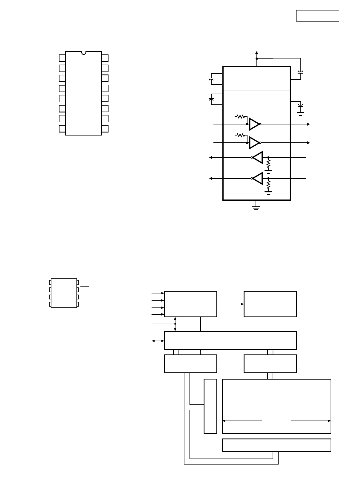
M24C64 (IC 404) FRONT P.W.B
1
E0 V
2
3
E2
4
SS
8
CC
7
WCE1
6
SCL
5
SDAV
Block Diagram
WC
E0
E1
E2
SCL
SDA
Control Logic
Address Register
and Counter
I/O Shift Register
Y Decoder
High Voltage
Generator
Data
Register
1 Page
15
X Decoder
CXA1511M (IC 201) XM-READY P.W.B.
85
Block Diagram and Pin Configuration
DRA-697CI
IN
1
4
Photo
Diode
1
NJM2068 (IC 104-114, 120) INPUT P.W.B.
(IC 209) XM-READY P.W.B.
Delector &
Head
Amp
ABLC
2
C1 C2GND fo N.C. V
470, 680
Limiter
Amp
BPF
BEF
Comparator
3
0.01µ0.01µ
4
Integralor
6
5
Hysteresis
Comparator
200k
(fo = 40kHz)
7
OUT
8
CC
V
CC
=5V
16
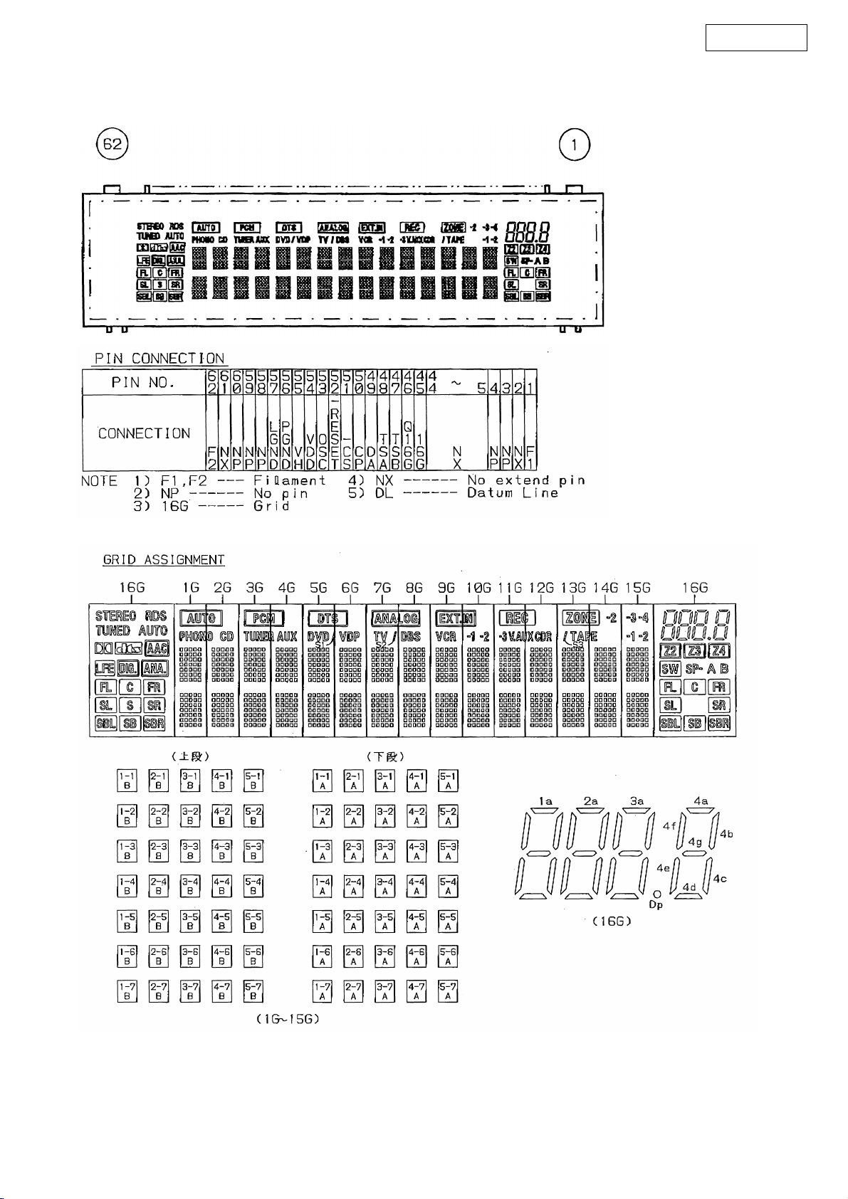
2. FL DISPLAY
16-ST-87GINK (FLT301)
DRA-697CI
17
 Loading...