

Page 1
e
SERVICE MANUAL
MODEL JP E3 E2 EK EA E1 E1C E1K
Ver. 3
Please refer to the
MODIFICATION NOTICE.
AVR-X1100W
AVR-S700W
INTEGRATED NETWORK AV RECEIVER
P P P P P
P
• For purposes of improvement, specications and design are subject to change without notice.
Please use this service manual with referring to the operating instructions without fail.
•
Some illustrations using in this service manual are slightly different from the actual set.
•
e
D&M Holdings Inc.
S0879-1V03DM/DG1407
Copyright 2014 D&M Holdings Inc. All rights reserved.
WARNING: Violators will be prosecuted to the maximum extent possible.
Page 2

CONTENTS
ABOUT THIS MANUAL
What you can do with this manual ............................................3
Using Adobe Reader (Windows version) ..................................4
SAFETY PRECAUTIONS
NOTE FOR SCHEMATIC DIAGRAM
NOTE FOR PARTS LIST
TECHNICAL SPECIFICATIONS for AVR-X1100W
DIMENSION for AVR-X1100W
TECHNICAL SPECIFICATIONS for AVR-S700W
DIMENSION for AVR-S700W
Precautions During Service
Initializing This Unit .................................................................11
Service Jigs .............................................................................11
DISASSEMBLY
1. FRONT PANEL ASSY ........................................................13
2. DIGITAL PCB .....................................................................14
3. RADIATOR ASSY ...............................................................15
4. SMPS PCB .........................................................................15
5. REGULATOR PCB .............................................................15
6. TRANS POWER ................................................................15
SPECIAL MODE
Special Mode Conguration Buttons (for AVR-X1100W) .........16
Special Mode Conguration Buttons (for AVR-S700W) ..........17
1. Version Display Mode ........................................................18
2. PANEL / REMOTE LOCK Selection Mode .........................22
3. Selection Modes for Service-related Operations ................23
DIAGNOSTIC PATH DIAGRAM .........................................27
4. Remote ID Setup Mode ......................................................49
5. Protection Pass Mode ........................................................50
6. CX870 / CY920 Reboot mode ............................................50
7. CX870 / CY920 Initialization mode ....................................51
Service Jigs
Procedure after Replacing the Microprocessor, etc.
Firmware Update Procedure
1. Updating by USB ................................................................54
2. Updating by DPMS .............................................................63
ADJUSTMENT
SURROUND MODES AND PARAMETERS
.............................................................................52
.........................................................................70
.............................................................3
..........................................................6
.........................................7
...........................................................7
..................9
.................................................9
..................10
.................................................10
...................................................11
........................................................................12
......................................................................16
..........54
..................................................54
............................71
TROUBLE SHOOTING
1. POWER ..............................................................................74
2. Analog video ......................................................................75
3. HDMI/DVI ...........................................................................76
4. AUDIO ................................................................................78
5. Network/Bluetooth/USB .....................................................81
6. SMPS .................................................................................84
CLOCK FLOW & WAVE FORM IN DIGITAL BLOCK
LEVEL DIAGRAM
BLOCK DIAGRAM
POWER DIAGRAM
WIRING DIAGRAM
PRINTED WIRING BOARDS
SCHEMATIC DIAGRAMS (1/19)
SCH01_HDMI_RX ................................................................100
SCH02_HDMI ADV7623 .......................................................101
SCH03_HDMI_TX .................................................................102
SCH04_DIGITAL SUPPLY ....................................................103
SCH05_MCU ........................................................................104
SCH06_MCU_LEVEL_CHG .................................................105
SCH07_DIR_PLD .................................................................106
SCH08_DSP .........................................................................107
SCH09_MAIN DAC ...............................................................108
SCH10_NETWORK ..............................................................109
SCH11_FRONT_HDMI .........................................................110
SCH12_ANALOG .................................................................. 111
SCH13_ADAPTER ................................................................11 2
SCH14_BLUETOOTH ...........................................................11 3
SCH15_DIFF-AMP ................................................................11 4
SCH16_MAIN ........................................................................11 5
SCH17_FRONT ....................................................................11 6
SCH18_REGULATOR ...........................................................117
SCH19_SMPS ......................................................................11 8
EXPLODED VIEW
PACKING VIEW
SEMICONDUCTORS
1. IC's ...................................................................................122
2. FL DISPLAY .....................................................................148
............................................................74
.............86
....................................................................87
...................................................................93
..................................................................94
..................................................................95
...................................................96
...........................................100
.................................................................11 9
.....................................................................121
.............................................................122
2
Page 3
ABOUT THIS MANUAL
Read the following information before using the service manual.
What you can do with this manual
Search for a Ref. No. (phrase)
(Ctrl+Shift+F)
You can use the search function in Acrobat Reader to
search for a Ref. No. in schematic diagrams, printed
wiring circuit diagrams, block diagrams, and parts
lists.
1.Press
• The Search window appears.
2.EntertheRef.No.youwanttosearchforinthe
Search window, and then click the
•A list of search results appears.
Ctrl+Shift+F
Shift
Ctrl
onthekeyboard.
F
Search
button.
Jump to the target of a schematic
diagram connector
Click the Ref. No. of the target connector in the red
box around a schematic diagram connector.
•The screen jumps to the target connector.
CP401
v
CP106
3.Click an item on the list.
• The screen jumps to the page for that item, and the
searchphraseisdisplayed.
•Pagemagnicationstaysthesameasbeforethe
jump.
3
Page 4
Using Adobe Reader (Windows version)
Add notes to this data (Sign)
TheSignfunctionletsyouaddnotestothedatain
this manual.
Savetheleonceyouhavenishedaddingnotes.
[Example using Adobe Reader X]
"View"
On the
• The Sign pane appears.
[Example using Adobe Reader 9]
On the
menu, click
"Document"
"Sign"
menu, click
.
"Sign"
.
Magnify schematic / printed circuit
board diagrams - 1
(Ctrl+Space, mouse operation)
Ctrl+Space
Press
mousetoselecttheareayouwanttoview.
• Theselectedareaismagnied.
• Whenyouwanttomovetheareashown,hold
Space
down
• Whenyouwanttoshowafullpageview,press
Ctrl+0
onthekeyboard.
onthekeyboardanddragthe
0
Ctrl Space
and drag the mouse.
Print a magnied part of the manual
ThePropertiesdialogboxandfunctionswillvarydependingonyourprinter.
1. Dragthemousetomagnifythepartyouwanttoprint.
2. On the
3. CongurethefollowingsettingsinthePrintdialogbox.
"File"
menu, click
"Print"
.
• Properties
Click this button and check that the printer is set to a
suitable paper size.
• Page to print
Select the following checkbox.
More Options
"
• Page Sizing & Handling
Select the following checkbox.
Size
"
Size Options
" / "
Current View
" : "
" : "
Fit
"
"
4. Click the
Print
button to start printing.
4
Page 5
Magnify schematic / printed circuit
board diagrams - 2
(Pan & Zoom function)
ThePan&Zoomfunctionletsyouseewhichpartof
amagnieddiagramisbeingshowninaseparate
window.
[Example using Adobe Reader X]
"View"
On the
"Pan & Zoom"
menu, point to
.
"Zoom"
, and then click
Magnify schematic / printed circuit
board diagrams - 3
(Loupe Tool function)
TheLoupeToolfunctionletsyoumagnifyaspecic
part of a diagram in a separate window.
[Example using Adobe Reader X]
"View"
On the
"Loupe Tool"
menu, point to
.
"Zoom"
, and then click
• The Pan & Zoom window appears on the screen.
[Example using Adobe Reader 9]
"Tools"
On the
then click
menu, point to
"Pan & Zoom Window"
"Select & Zoom"
.
, and
• The Loupe Tool window appears on the screen.
[Example using Adobe Reader 9]
"Tools"
On the
then click
menu, point to
"Loupe Tool Window"
"Select & Zoom"
.
, and
5
Page 6

SAFETY PRECAUTIONS
The following items should be checked for continued protection of the customer and the service technician.
leakage current check
Beforereturningthesettothecustomer,besuretocarryouteither(1)aleakagecurrentcheckor(2)alinetochassis
resistance check. If the leakage current exceeds 0.5 milliamps, or if the resistance from chassis to either side of the
power cord is less than 460 kohms, the set is defective.
Be sure to test for leakage current with the AC plug in both polarities, in addition, when the set's power is in each state
(on,offandstandbymode),ifapplicable.
CAUTION
Please heed the following cautions and instructions during servicing and
inspection.
◎Heed the cautions!
Cautions which are delicate in particular for servicing
are labeled on the cabinets, the parts and the chassis,
etc. Be sure to heed these cautions and the cautions
described in the handling instructions.
◎Cautions concerning electric shock!
(1) AnACvoltageisimpressedonthisset,soifyou
touch internal metal parts when the set is energized,
youmaygetanelectricshock.Avoidgettingan
electricshock,byusinganisolatingtransformer
and wearing gloves when servicing while the set is
energized,orbyunpluggingthepowercordwhen
replacing parts, for example.
(2) Therearehighvoltagepartsinside.Handlewith
extra care when the set is energized.
◎ Caution concerning disassembly and
assembly!
Through great care is taken when parts were
manufacturedfromsheetmetal,theremaybeburrson
theedgesofparts.Theburrscouldcauseinjuryifngers
are moved across them in some rare cases. Wear gloves
toprotectyourhands.
◎Use only designated parts!
Theset'spartshavespecicsafetyproperties(re
resistance,voltageresistance,etc.).Besuretouseparts
which have the same properties for replacement. The
burrs have the same properties. In particular, for the
importantsafetypartsthatareindicatedbythez mark
on schematic diagrams and parts lists, be sure to use
the designated parts.
◎ Be sure to mount parts and arrange the wires
as they were originally placed!
Forsafetyseasons,somepartsusetapes,tubesorother
insulatingmaterials,andsomepartsaremountedaway
from the surface of printed circuit boards. Care is also
takenwiththepositionsofthewiresbyarrangingthem
andusingclampstokeepthemawayfromheatingand
highvoltageparts,sobesuretoseteverythingbackas
itwasoriginallyplaced.
◎Make a safety check after servicing!
Check that all screws, parts and wires removed or
disconnected when servicing have been put back in their
original positions, check that no serviced parts have
deteriorate the area around. Then make an insulation
check on the external metal connectors and between
the blades of the power plug, and otherwise check that
safetyisensured.
(Insulationcheckprocedure)
Unplug the power cord from the power outlet, disconnect
the antenna, plugs, etc., and on the power. Using a 500V
insulation resistance tester, check that the insulation
resistancevaluebetweentheinplugandtheexternally
exposedmetalparts(antennaterminal,headphones
terminal,inputterminal,etc.)is1MΩorgreater.Ifitis
less, the set must be inspected and repaired.
CAUTION
Concerning important
safety parts
Manyoftheelectricandthestructuralpartsusedinthe
sethavespecialsafetyproperties.Inmostcasesthese
propertiesaredifculttodistinguishbysight,andtheuse
ofreplacementpartswithhigherratings(ratedpower
andwithstandvoltage)doesnotnecessarilyguarantee
thatsafetyperformancewillbepreserved.Partswith
safetypropertiesareindicatedasshownbelowonthe
wiring diagrams and the parts list in this service manual.
Be sure to replace them with the parts which have the
designated part number.
(1) Schematicdiagrams .......Indicatedbythez mark.
(2) Partslists .......Indicatedbythez mark.
The use of parts other than the
designated parts could cause electric
shocks,resorotherdangerous
situations.
6
Page 7
NOTE FOR SCHEMATIC DIAGRAM
WARNING:
Partsindicatedbythezmarkhavecriticalcharacteristics.UseONLYreplacementpartsrecommendedbythemanufacturer.
CAUTION:
Beforereturningthesettothecustomer,besuretocarryouteither(1)aleakagecurrentcheckor(2)alinetochassisresistancecheck.
If the leakage current exceeds 0.5 milliamps, or if the resistance from chassis to either side of the power cord is less than 460 kohms, the
set is defective.
WARNING:
DONOTreturnthesettothecustomerunlesstheproblemisidentiedandremedied.
NOTICE:
ALLRESISTANCEVALUESINOHM.k=1,000OHM/M=1,000,000OHM
ALLCAPACITANCEVALUESAREEXPRESSEDINMICROFARAD,UNLESSOTHERWISEINDICATED.PINDICATESMICRO-MICRO
FARAD.EACHVOLTAGEANDCURRENTAREMEASUREDATNOSIGNALINPUTCONDITION.CIRCUITANDPARTSARESUBJECT
TOCHANGEWITHOUTPRIORNOTICE.
NOTE FOR PARTS LIST
1.Partsindicatedby
2.Whenorderingapart,makeacleardistinctionbetween"1"and"I"(i)toavoidmis-supplying.
3.Apartorderedwithoutspecifyingitspartnumbercannotbesupplied.
4.Partindicatedby"★" mark is not illustrated in the exploded view.
WARNING:
Partsindicatedbythezmarkhavecriticalcharacteristics.UseONLYreplacementpartsrecommendedbythemanufacturer.
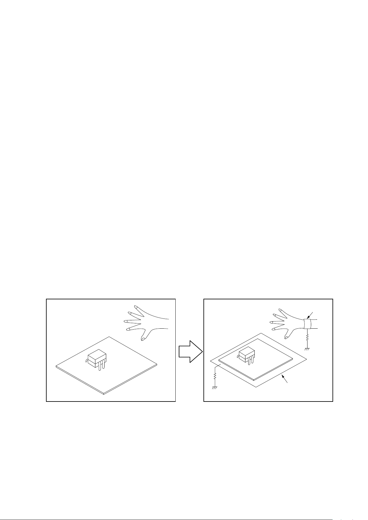
INSTRUCTIONS FOR HANDLING SEMI-CONDUCTORS AND OPTICAL UNIT
Electrostaticbreakdownofthesemi-conductorsoropticalpickupmayoccurduetoapotentialdifferencecausedby
electrostatic charge during unpacking or repair work.
"nsp"
on this table cannot be supplied.
1. GroundforHumanBody
Besuretowearagroundingband(1MΩ)thatisproperlygroundedtoremoveanystaticelectricitythatmaybe
chargedonthebody.
2. GroundforWorkbench
Besuretoplaceaconductivesheetorcopperplatewithpropergrounding(1MΩ)ontheworkbenchorothersurface,
wherethesemi-conductorsaretobeplaced.Becausethestaticelectricitychargeonclothingwillnotescapethrough
thebodygroundingband,becarefultoavoidcontactingsemi-conductorswithyourclothing
<Incorrect>
<Correct>
CBA
CBA
1MΩ
Grounding Band
1MΩ
Conductive Sheet or
Copper Plate
7
Page 8

Personal notes:
8
Page 9
TECHNICAL SPECIFICATIONS FOR AVR-X1100W
nAudio section
• Power amplifier
Rated output
Front :
80W+80W(8Ω、20Hz~20kHz with 0.08% T.H.D.)
120W+120W(6Ω、1kHz with 0.7% T.H.D)
Center :
80W(8Ω、20Hz~20kHz with 0.05% T.H.D.)
120W(6Ω、1 kHz with 0.7 % T.H.D.)
Surround :
80W+80W(8Ω、20 Hz – 20 kHz with 0.08% T.H.D.)
120W+120W(6Ω、1 kHz with 0.7 % T.H.D.)
Surround back:
80W+80W(8Ω、20 Hz – 20 kHz with 0.08% T.H.D.)
120W+120W(6Ω、1 kHz with 0.7 % T.H.D.)
Output connectors : 4~16Ω
:
nAnalog section
Input sensitivity/Input impedance : 200 mV/47 kΩ
Frequency response : 10 Hz – 100 kHz — +1, –3 dB(Direct mode)
S/N : 98 dB(IHF–A weighted, Direct mode)
nVideo section
Input/output level and impedance : 1 Vp-p, 75 Ω
Frequency response : 5 Hz – 10 MHz — 0, –3 dB
nTuner section
Reception frequency range : FM 87.5 MHz – 107.9 MHz(for E3)
Effective sensitivity : FM 1.2μV(12.8dBf)
50 dB sensitivity : MONO ― 2.8 μV (20.2 dBf)
S/N: MONO ― 70 dB (IHF–A weighted, Direct mode)
STEREO ― 67 dB (IHF–A weighted, Direct mode)
Distortion : MONO ― 0.7 % (1 kHz)
SRETEO ― 1.0 % (1 kHz)
FM 87.5 MHz – 108.0 MHz(for E2,E1. E1C)
FM 76.0 MHz – 90.0 MHz(for JP)
AM 520 kHz – 1710 kHz(for E3)
AM 522 kHz – 1611 kHz(for E2,E1. E1C)
AM 522 kHz – 1629 kHz(for JP)
AM 18 μV
nWireless LAN section
Network type
(wireless LAN standard): Conforming to Wi-Fi®z1
Security : WEP 64 bit, WEP 128 bit
Radio frequency : 2.4 GHz
No. of channels : 1 – 11 ch (for E3)
z1 The Wi-Fi® CERTIFIED Logo and the Wi-Fi CERTIFIED On-Product
WPA/WPA2-PSK (AES)
WPA/WPA2-PSK (TKIP)
1 – 13 ch (for E2, E1, E1C, JP)
Logo are registered trademarks of the Wi-Fi Alliance.
nBluetooth section
Communications system : Bluetooth Version 2.1 + EDR
Transmission power : Maximum 2.5 mW (Class 2)
Maximum communication range : Approx. 32.8 ft/10m 2 in line of sight
Frequency band : 2.4 GHz band
Modulation scheme : FHSS (Frequency-Hopping Spread Spectrum)
Supported proles : A2DP 1.2 (Advanced Audio Distribution Prole)
Corresponding codec : SBC, AAC
Transmission range (A2DP) : 20 Hz - 20,000 Hz
nGeneral
Power supply : (for E3) : AC 120 V, 60 Hz
Power consumption : 430W
Power consumption in standby mode : 0.1W
Power consumption in CEC standby mode : 0.5W
Power consumption in network standby mode : 2.7W
(for E2/E1) : AC 230 V, 50 Hz / 60Hz
(for E1C) : AC 220 V, 50 Hz
(for JP) : AC 100V、50/60Hz
(Enhanced Data Rate)
AVRCP 1.4 (Audio Video Remote Control Prole)
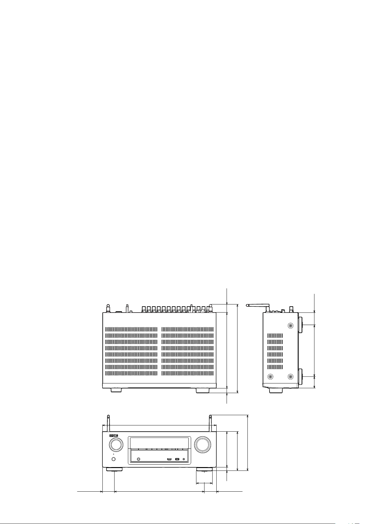
DIMENSION FOR AVR-X1100W
Unit: Unit : in. (mm) Weight: 18 lb 15 oz (8.6 kg)
17 3/32 (434)
(32)
1 7/32
11 11/32 (288)
13 11/32 (339)
3/4
(19)
(47)
1 27/32
7 3/4 (197)
(44)
1 47/64
5 23/64 (136)
5 15/16 (151)
2 23/64
(60)
1 49/64 (45) 1 49/64 (45)
13 35/64 (344)
(15)
19/32
9
8 15/32 (215)
Page 10
TECHNICAL SPECIFICATIONS FOR AVR-S700W
nAudio section
• Power amplifier
Rated output
Front :
75W+75W(8Ω、20Hz~20kHz with 0.08% T.H.D.)
110W+110W(6Ω、1kHz with 0.7% T.H.D)
Center :
75W(8Ω、20Hz~20kHz with 0.05% T.H.D.)
110W(6Ω、1 kHz with 0.7 % T.H.D.)
Surround :
75W+75W(8Ω、20 Hz – 20 kHz with 0.08% T.H.D.)
110W+110W(6Ω、1 kHz with 0.7 % T.H.D.)
Surround back:
75W+75W(8Ω、20 Hz – 20 kHz with 0.08% T.H.D.)
110W+110W(6Ω、1 kHz with 0.7 % T.H.D.)
Output connectors : 4~16Ω
:
nAnalog section
Input sensitivity/Input impedance : 200 mV/47 kΩ
Frequency response : 10 Hz – 100 kHz — +1, –3 dB(Direct mode)
S/N : 98 dB(IHF–A weighted, Direct mode)
nVideo section
Input/output level and impedance : 1 Vp-p, 75 Ω
Frequency response : 5 Hz – 10 MHz — 0, –3 dB
nTuner section
Reception frequency range : FM 87.5 MHz – 107.9 MHz
Effective sensitivity : FM 1.2μV(12.8dBf)
50 dB sensitivity : MONO ― 2.8 μV (20.2 dBf)
S/N: MONO ― 70 dB (IHF–A weighted, Direct mode)
STEREO ― 67 dB (IHF–A weighted, Direct mode)
Distortion : MONO ― 0.7 % (1 kHz)
SRETEO ― 1.0 % (1 kHz)
AM 520 kHz – 1710 kHz
AM 18 μV
nWireless LAN section
Network type
(wireless LAN standard): Conforming to Wi-Fi®z1
Security : WEP 64 bit, WEP 128 bit
Radio frequency : 2.4 GHz
No. of channels : 1 – 11 ch
z1 The Wi-Fi® CERTIFIED Logo and the Wi-Fi CERTIFIED On-Product
WPA/WPA2-PSK (AES)
WPA/WPA2-PSK (TKIP)
Logo are registered trademarks of the Wi-Fi Alliance.
nBluetooth section
Communications system : Bluetooth Version 2.1 + EDR
Transmission power : Maximum 2.5 mW (Class 2)
Maximum communication range : Approx. 32.8 ft/10m 2 in line of sight
Frequency band : 2.4 GHz band
Modulation scheme : FHSS (Frequency-Hopping Spread Spectrum)
Supported proles : A2DP 1.2 (Advanced Audio Distribution Prole)
Corresponding codec : SBC, AAC
Transmission range (A2DP) : 20 Hz - 20,000 Hz
nGeneral
Power supply : (for E3) : AC 120 V, 60 Hz
Power consumption : 400W
Power consumption in standby mode : 0.1W
Power consumption in CEC standby mode : 0.5W
Power consumption in network standby mode : 2.7W
(Enhanced Data Rate)
AVRCP 1.4 (Audio Video Remote Control Prole)
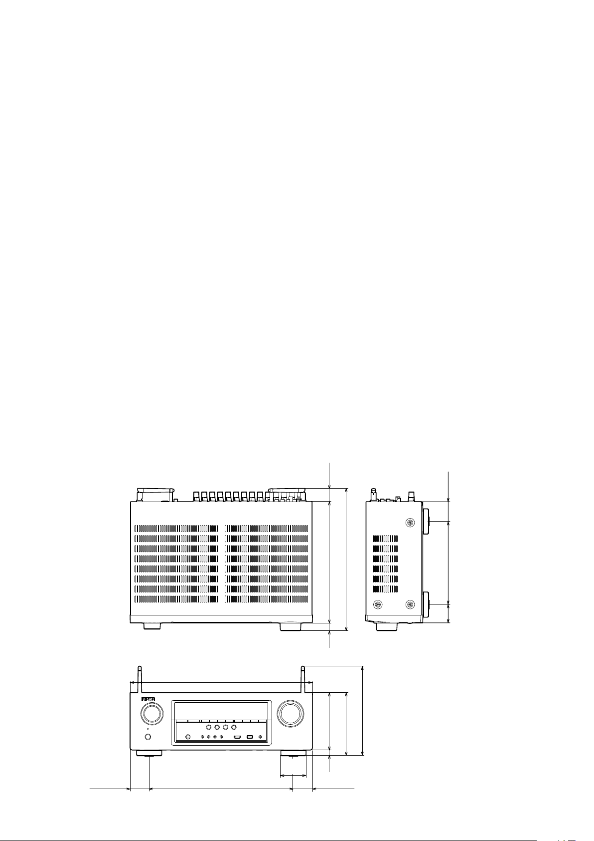
DIMENSION FOR AVR-S700W
Unit: Unit : in. (mm) Weight: 18 lb 15 oz (8.6 kg)
17 3/32 (434)
(32)
1 7/32
11 11/32 (288)
13 11/32 (339)
3/4
(19)
(47)
1 27/32
7 3/4 (197)
(44)
1 47/64
5 23/64 (136)
5 15/16 (151)
2 23/64
(60)
1 49/64 (45) 1 49/64 (45)
13 35/64 (344)
(15)
19/32
10
8 15/32 (215)
Page 11
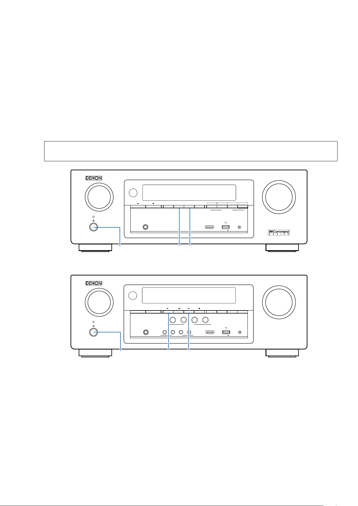
PRECAUTIONS DURING SERVICE
Initializing This Unit
Initialize this unit if you have replaced the microcomputer, one of the parts around the microcomputer, or the digital PCB.
1. Press the power button to turn off the power.
2. AVR-X1100W
Hold down buttons "
ZONE2 SOURCE
power.
AVR-S700W
Hold down buttons
TUNER PRESET CH +
power.
3. Release the buttons after conrming that the display ashes in intervals of approximately 1 second.
The unit is initialized.
*
" and "
DIMMER
and "
" at the same time and press the power button to turn on the
TUNE -
" at the same time and press the power button to turn on the
NOTE:
• If the status in step 3 does not occur, start again from step 1.
• Initializing the device restores settings congured by the user to the factory settings. Take note of your settings beforehand
and recongure them after initialization.
AVR-X1100W
AVR-S700W
SOURCE SELECT
SOURCE SELEC T
PRESET CH
PHONES
MASTER VOLUME
ZONE2
TUNER
ZONE2
ON/OFF
DIMMER STATUS
SOURCE
CBL/SAT
DVD/Blu-ray
QUICK SELECT
5V/ 1A
MEDIA
321 4
PLAYER
ONLINE
SETUP MICAUX - HDMI
DIMMERX ZONE2 SOURCE
MASTER VOLUM E
TUNER
PRESET CH
CB L /S A T
1
PHONES
MOVIE MUSIC GAME PURE
SOUND MODE
TUNEZONE2 ON/OFF ZONE2 SOURCE
BAND MODE DIMMER STATUS
DVD/Blu-ray
2
QUICK SELECT
ONLINE
GAME
3
4
SETUP MICAUX - HDMI
5V/ 1A
X TUNER PRESET CH +
TUNING
-
Service Jigs
The following jigs (extension cable kit) are used when repairing the PCB.
Order the jigs from your dealer if necessary.
8U- 110084S : EXTENSION UNIT KIT : 1 Set
(See 52 page)
11
Page 12
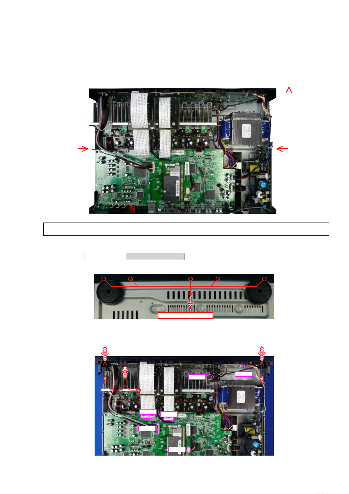
DISASSEMBLY
• Remove each part in the order of the arrows below.
• Reassemble removed parts in the reverse order.
• Read
"Precautions During Work"
• If wire bundles are removed or moved during adjustment or part replacement, reshape the wires after completing the
work. Failure to shape the wires correctly may cause problems such as noise.
before reassembling removed parts.
TOP COVER
FRONT PANEL ASSY
See "
DISASSEMBLY
1. FRONT PANEL ASSY
and "
EXPLODED VIEW
FRONT PCB
(Ref. No. of EXPLODED VIEW : P1)
ENCODER&POWER PCB
(Ref. No. of EXPLODED VIEW : P2)
PHONE PCB
(Ref. No. of EXPLODED VIEW : P3)
iPODUSB_MIC PCB
(Ref. No. of EXPLODED VIEW : P4)
HDMI_FFC_CABLE PCB
(Ref. No. of EXPLODED VIEW : P5)
FRONT_HDMI PCB
(Ref. No. of EXPLODED VIEW : P6)
BLUETOOTH PCB
(Ref. No. of EXPLODED VIEW : P7)
"
"
DIGITAL PCB ASSY
See "
DISASSEMBLY
2. DIGITAL PCB ASSY
and "
EXPLODED VIEW
DIGITAL PCB
(Ref. No. of EXPLODED VIEW : P17)
ADAPTER PCB
(Ref. No. of EXPLODED VIEW : P18)
CX870 MODULE
(Ref. No. of EXPLODED VIEW : P19)
TUNER PCB
(Ref. No. of EXPLODED VIEW : P20)
RADIATOR ASSY
See "
DISASSEMBLY
3. RADIATOR ASSY
and "
EXPLODED VIEW
MAIN PCB
(Ref. No. of EXPLODED VIEW : P8)
HDMI CABLE GUIDE PCB
(Ref. No. of EXPLODED VIEW : P9)
FRONT CABLE GUIDE PCB
(Ref. No. of EXPLODED VIEW : P10)
BT WIRE GUIDE PCB
(Ref. No. of EXPLODED VIEW : P11)
BAIS TR PCB
(Ref. No. of EXPLODED VIEW : P12)
TEMP_DETECT PCB
(Ref. No. of EXPLODED VIEW : P13)
DIFF-AMP PCB
(Ref. No. of EXPLODED VIEW : P16)
PHONE WIRE GUIDE PCB
(Ref. No. of EXPLODED VIEW : P22)
"
"
"
"
SMPS PCB
See "
DISASSEMBLY
4. SMPS PCB
and "
EXPLODED VIEW
SMPS PCB
(Ref. No. of EXPLODED VIEW : P14)
REGULATOR PCB
See "
DISASSEMBLY
5. REGULATOR PCB
and "
EXPLODED VIEW
REGULATOR PCB
(Ref. No. of EXPLODED VIEW : P15)
TRANS POWER
See "
DISASSEMBLY
5. TRANS POWER
and "
EXPLODED VIEW
TRANS POWER
(Ref. No. of EXPLODED VIEW : P21)
"
"
"
"
"
"
12
Page 13
Explanatory Photos for DISASSEMBLY
View from the bottom
• The angles from which the photos are taken are shown by "
• See the diagram below about the shooting direction of each photograph.
• Photographs with no shooting direction indicated were taken from the top of the unit.
• The photograph is AVR-S700E3 model.
Photo angle: A, B, C, D
The viewpoint of each photograph
(Shooting direction:X)[View from the top]
↓Shooting direction: B↓
".
Front side
Shooting
direction: D
↑Shooting direction: A↑
Caution:・Before disassembling this unit, be sure to discharge the power line (the colored line in the schematic diagram).
FFC cables with one end disconnected should be insulated by using tapes, etc.
・
Shooting
direction: C
1. FRONT PANEL ASSY
Proceeding : TOP COVER
(1) Remove the screws.
FRONT PANEL ASSY
→
(2) Remove the connector wire and FFC. Remove the screws.
Front side
FFC
CN619
FFC
CN914
13
CN104
CN102
Page 14
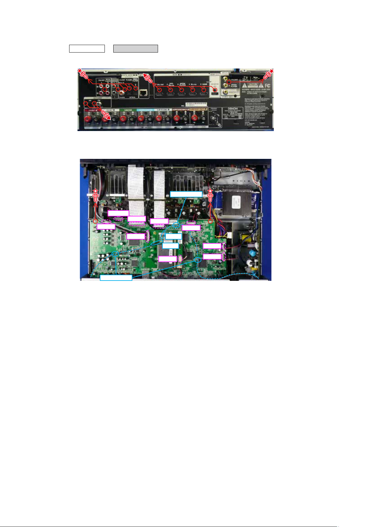
2. DIGITAL PCB
Proceeding : TOP COVER
(1) Remove the screws.
(2) Remove the connector wire and FFC. Remove the screws.
CN761
DIGITAL PCB
→
CN8221
FFC
CN619
Front side
STYLE PIN
FFC
CON1
CON2
CN914
CN762
CN741
CN823
STYLE PIN
14
Page 15
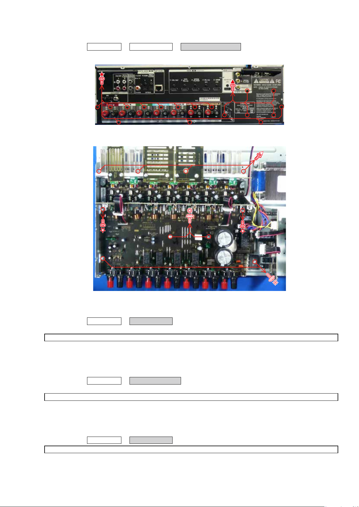
3. RADIATOR ASSY
Proceeding : TOP COVER
(1) Remove the screws.
(2) Remove the screws.
DIGITAL PCB
→
RADIATOR ASSY
→
Front side
4. SMPS PCB
Proceeding : TOP COVER
(1) Remove the connector wire. Remove the screws.
See "EXPLODED VIEW" for instructions on how to remove each PCB of the "
→
SMPS PCB
5. REGULATOR PCB
Proceeding : TOP COVER
(1) Remove the connector wire. Remove the screws.
See "EXPLODED VIEW" for instructions on how to remove each PCB of the "
REGULATOR PCB
→
6. TRANS POWER
Proceeding : TOP COVER→TRANS POWER
See "EXPLODED VIEW" for instructions on how to remove each PCB of the "
SMPS PCB
REGULATOR PCB
TRANS POWER
".
".
".
15
Page 16
SPECIAL MODE
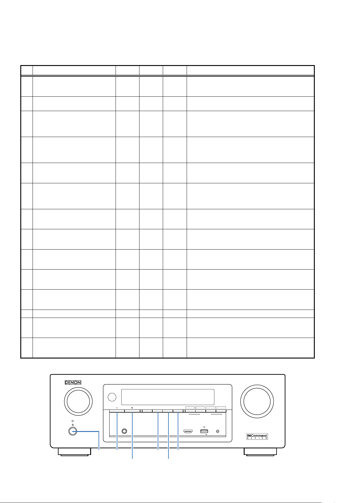
Special Mode Conguration Buttons (for AVR-X1100W)
No. 1 - 13 : Hold down buttons A, B and C at the same time and press the power button to turn on the power.
b
No. 14 : Press the A and B buttons simultaneously while inserting the AC plug to turn the power on.
b
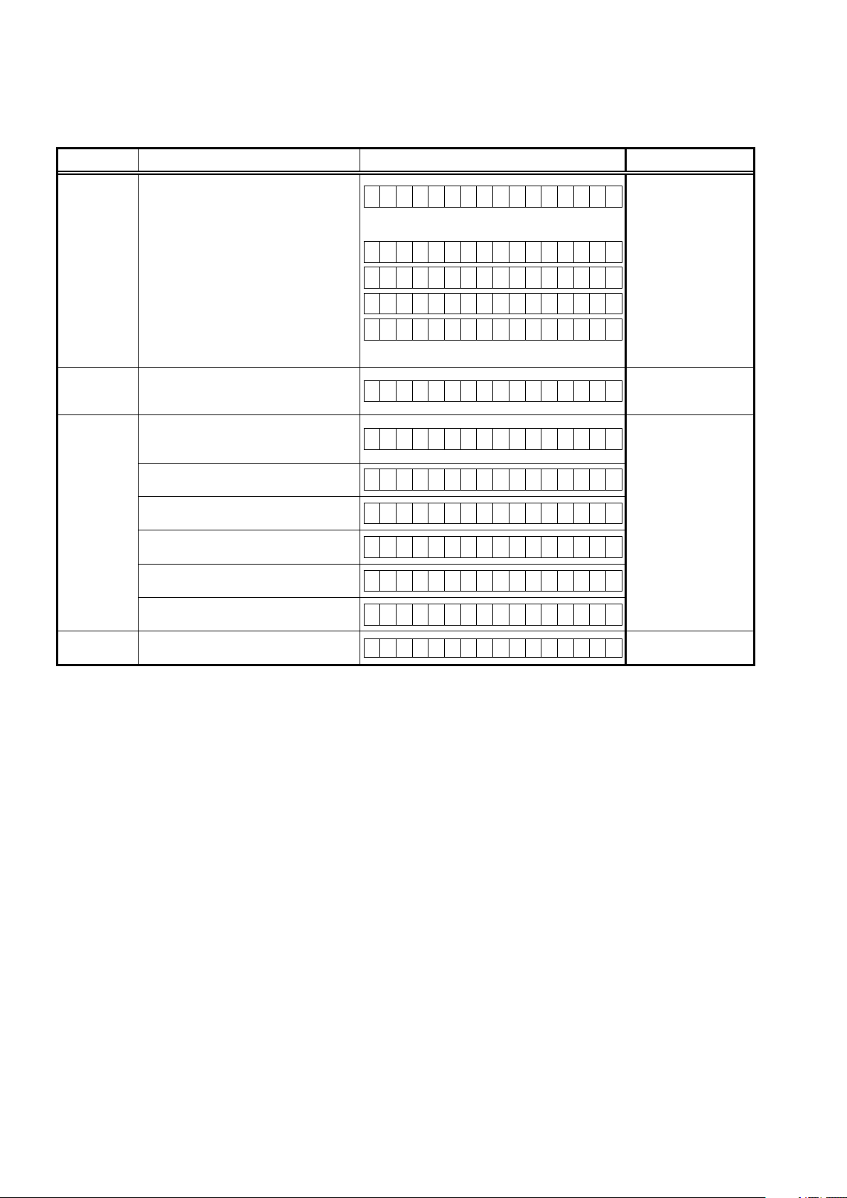
No. Mode Button A Button B Button C Contents
Version Display
1
(u-COM / DSP Error Display)
2 Protection History Display Mode
Check the Video/Audio pass
3
Mode
4 Remote ID Setup Mode
5 TUNER step
6 Operation INFO
User Initialization mode
7
(Settings for the Installer Setup are
not initialized.)
Factory Initialization mode
8
(Initialization includes settings for the
Installer Setup.)
Mode for preventing remote
9
control acceptance
PANEL LOCK mode
10
(with Volume)
PANEL LOCK mode
11
(without Volume)
12 Panel Lock Release
13 Protection pass mode
14 Forced USB All Device Write Mode
DIMMER STATUS –
ZONE2
SOURCE
DIMMER STATUS
↑ ↑ ↑
↑ ↑ ↑
↑ ↑ ↑
↑ ↑ ↑
TUNER
PRESET
CH -
ZONE2
SOURCE
TUNER
PRESET
CH +
TUNER
PRESET
CH +
DIMMER -
ZONE2
SOURCE
↑ ↑ -
↑ ↑ -
↑ ↑ -
TUNER
PRESET
CH +
ZONE2
SOURCE
STATUS
TUNER
PRESET
STATUS -
CH +
Displays the version of rmware such as the main rmware
or DSP, etc. Errors that have occurred are displayed. (See
18 page)
Displays the protection occurrence history.
(See 45 page)
This is a special mode for service conrmation used during
repair work to simplify the conrmation work for the Audio
channel/video channel.
(See 25 page)
If there are multiple DENON AV receivers in the same
area, this mode stops the other AV receivers from being
operated concurrently with this device.
(See 49 page)
Enables reception STEP of the ANALOG TUNER to be
changed.
(See 48 page)
Displays the total operating time of the set, number
of times the power was switched on, and number of
occurrences of each protection.
(See 47 page)
Initializes backup data.
-
(Settings for the Installer Setup are not initialized.)
Initializes backup data.
(Initialization includes settings for the Installer Setup.)
Start this unit in the PANEL/REMOTE LOCK selection
mode so that PANEL LOCK and Remote Lock can be
-
selected as ON or OFF. (See 22 page)
This function prevents reception of all keys/encoders
(including VOLUME) other than the power supply button
on the Front Panel.
This function prevents reception of all keys/encoders other
than the power supply button and VOLUME encoder on
the Front Panel.
Function for Releasing the PANEL LOCK
Enables the power to be turned on when protection
detection is in the stopped state.
(See 50 page)
Mode used when this unit cannot be recovered.
Forcibly switches this unit to USB update mode.
(See 56 page)
SOURCE SELECT
X
PRESET CH -
TUNER
PRESET CH
PHONES
TUNER
PRESET CH +
ZONE2
ZONE2
ON/OFF
SOURCE
ZONE2
SOURCE
DIMMER STATUS
STATUSTUNER
DIMMER
16
MASTER VOLUME
MEDIA
DVD/Blu-ray
CBL/SAT
QUICK SELECT
5V/ 1A
321 4
PLAYER
ONLINE
SETUP MICAUX - HDMI
Page 17
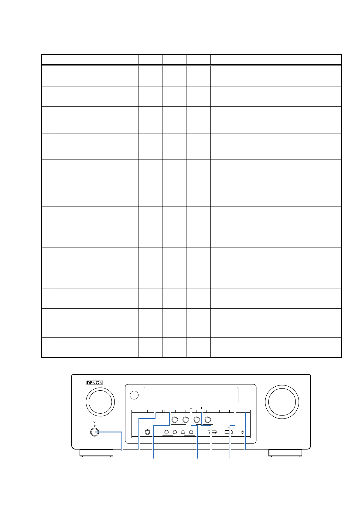
Special Mode Conguration Buttons (for AVR-S700W)
No. 1 - 13 : Hold down buttons A, B and C at the same time and press the power button to turn on the power.
b
No. 14 : Press the A and B buttons simultaneously while inserting the AC plug to turn the power on.
b
No. Mode Button A Button B Button C Contents
Version Display
1
(u-COM / DSP Error Display)
2 Protection History Display Mode
Check the Video/Audio pass
3
Mode
4 Remote ID Setup Mode
5 TUNER step
6 Operation INFO
User Initialization mode
7
(Settings for the Installer Setup are
not initialized.)
Factory Initialization mode
8
(Initialization includes settings for the
Installer Setup.)
Mode for preventing remote
9
control acceptance
PANEL LOCK mode
10
(with Volume)
PANEL LOCK mode
11
(without Volume)
12 Panel Lock Release
13 Protection pass mode
14 Forced USB All Device Write Mode
DIMMER STATUS –
TUNER
PRESET
TUNE - TUNE +
CH +
↑ ↑ ↑
↑ ↑ ↑
↑ ↑ ↑
↑ ↑ ↑
TUNER
PRESET
CH -
TUNER
PRESET
CH +
TUNER
PRESET
TUNE - -
CH +
ZONE2
SOURCE
TUNER
PRESET
CH +
↑ ↑ -
↑ ↑ -
↑ ↑ -
ZONE2
SOURCE
TUNE +
TUNER
PRESET
CH +
ZONE2
SOURCE
TUNE +
Displays the version of rmware such as the main rmware
or DSP, etc. Errors that have occurred are displayed. (See
18 page)
Displays the protection occurrence history.
(See 45 page)
This is a special mode for service conrmation used during
repair work to simplify the conrmation work for the Audio
channel/video channel.
(See 25 page)
If there are multiple DENON AV receivers in the same area,
this mode stops the other AV receivers from being operated
concurrently with this device.
(See 49 page)
Enables reception STEP of the ANALOG TUNER to be
changed.
(See 48 page)
Displays the total operating time of the set, number of times
the power was switched on, and number of occurrences of
each protection.
(See 47 page)
Initializes backup data.
-
(Settings for the Installer Setup are not initialized.)
Initializes backup data.
(Initialization includes settings for the Installer Setup.)
Start this unit in the PANEL/REMOTE LOCK selection
mode so that PANEL LOCK and Remote Lock can be
-
selected as ON or OFF. (See 22 page)
This function prevents reception of all keys/encoders
(including VOLUME) other than the power supply button on
the Front Panel.
This function prevents reception of all keys/encoders other
than the power supply button and VOLUME encoder on the
Front Panel.
Function for Releasing the PANEL LOCK
Enables the power to be turned on when protection
detection is in the stopped state.
(See 50 page)
Mode used when this unit cannot be recovered.
Forcibly switches this unit to USB update mode.
-
(See 56 page)
SOURCE SELEC T
X
SOURCE
PRESET CH
PHONES
TUNER
TUNER
PRESET CH
DVD/Blu-ray
CB L /S A T
2
1
MOVIE MUSIC GAME PURE
PRESET CH +
QUICK SELECT
SOUND MODE
TUNER
-
17
TUNEZONE2 ON/OFF ZONE2 SOURCE
GAME
3
TUNE
BAND MODE DIMMER STATUS
ONLINE
4
5V/ 1A
TUNE +
DIMMER
-
MASTER VOLUM E
SETUP MICAUX - HDMI
STATUSZONE2
Page 18
1. Version Display Mode
1.1. Actions
Version information is displayed when the device is started in this mode.
1.2. Starting up
Hold down buttons "
Press the "
A version list is also displayed on GUIs while the version appears on the display.
b
STATUS
DIMMER
" button after this to show the information in section 1.3 on the display.
1.3. Display Order
Error information(See
→ e Main μ-com → r Main 1st Boot Loader → t DSP ROM → y Audio PLD → u GUI SFLASH
→ i Ethernet 1st Boot Loader, Hardware ID → o Ethernet 2nd Boot Loader, Rhapsody Flag → Q0 Ethernet IMAGE → Q1
Ethernet MAC ADDRESS information → Q2 BT MAC Address information
Model destination information :
q
FLD
A V R - S 7 0 0 W E 3 *
FLD
A V R - X 1 1 0 0 W E 3 *
FLD
A V R - X 1 1 0 0 W E 2 *
FLD
A V R - X 1 1 0 0 W E 1 *
" and "
STATUS
1.4. Error display
" at the same time and press the power button to turn on the power.
) → q Model destination information → w Firmware Package Version
FLD
A V R - X 1 1 0 0 W E 1 C *
FLD
A V R - X 1 1 0 0 W J P *
Firmware Package Version :
w
FLD
P a c k a g e : * * * *
Main µ-com Version :
e
FLD
* : Main version,
Main 1st Boot Loader :
r
FLD
DSP ROM :
t
FLD
Audio PLD :
y
FLD
GUI SFLASH :
u
FLD
@ : Model code, $ : Brand code, \ : Region code, * : version
M a i n : * * * * # # # # *
#
Sub version
:
M a i n F B L : * * . * *
D S P : * * . * *
A u d i o P L D : * * . * *
G U I : @ @ $ \ * * * *
18
Page 19
Ethernet 1st Boot Loader, Hardware ID :
i
FLD
E t h e r n e t F B L
Press the "
FLD
* * * * * * - b d
Ethernet 2nd Boot Loader, Rhapsody Flag :
o
FLD
Press the "
FLD
Ethernet IMAGE :
Q0
FLD
Press the "
FLD
Ethernet MAC ADDRESS information :
Q1
FLD
E t h e r n e t S B L
B * * * * * * * * * * * * - 0 A
E t h e r n e t I M G
I * * * * * * * * * * * *
* N E T M A C A d d r e s s
STATUS
STATUS
STATUS
" button.
" button.
" button.
Press the "
FLD
BT MAC ADDRESS information :
Q2
FLD
Press the "
FLD
* * * * * * - * * * * * *
* B T M A C A d d r e s s
* * * * * * - * * * * * *
STATUS
STATUS
" button.
" button.
19
Page 20
1.4. Error display
See the table below for descriptions of displayed errors and countermeasures for these.
Display order is q,w,e,r.
Condition States Display TROUBLE SHOOTING
q
Firm Check
NG
w
DIR NG
e
DSP NG
r
EEPROM NG
The model name, brand name and
region information written in the rmware
are compared to the region settings in
the PCB.This error is displayed if the
information does not match.
"▲" or "▼" is displayed as the rst
character if the rmware is not correct (see
right section of table).
This error is displayed if there is no
response from the DIR.
The DSP FLAG0 port does not enter "Hi"
status even after executing a DSP reset
during a DSP code boot.
The DSP FLAG0 port does not enter "Hi"
status before issuing a DSP command.
ACK="Hi" does not occur during DSP data
reading, even when WRITE="Lo".
ACK="Lo" does not occur during DSP
data reading, even when REQ="Lo".
ACK="Hi" does not occur during DSP data
writing, even when WRITE="Hi".
ACK="Lo" does not occur during DSP
data writing, even when REQ="Lo".
An error occurred in a checksum of the
EEPROM(*** is a block address number).
F I R M E R R O R
–
M a i n : * * * * * * * *
–
D S P : * * . * *
–
A u d i o P L D : * * . * *
–
G U I : * * * * * * * *
D I R E R R O R 0 1
D S P E R R O R 0 1
D S P E R R O R 0 2
D S P E R R O R 0 3
D S P E R R O R 0 4
D S P E R R O R 0 5
D S P E R R O R 0 6
E 2 P R O M E R R * * *
• Check the resistor for
setting region(R7581 /
R7582, DIGITAL PCB).
• Write the rmware for
the correct region.
• Check the DIR (IC772,
DIGITAL PCB) and
surrounding circuits.
• Check the DSP (IC781,
DIGITAL PCB) and
surrounding circuits.
20
Page 21
1.5. Version Display in the Setup Menu
Follow the steps below to display the rmware information.
(1) Press the "
(2) Select "
SETUP
" button on the remote control.
General - Information - Firmware
".
The version information is displayed as a 12-digit number as shown in the screenshot below.
General/Firmware
Version
XXXX - XXXX - XXXX
GUI Image
This 12-digit number comprises part of the version number of each device and module.
These version numbers correspond to the 12-digit number as shown below.
Mainμcom 0 0 2 3 0 0 1 6
The 6th digit from the right for Main μcom
The 5th digit from the right for Main μcom
The 2nd digit from the right for Main μcom
The 1st digit from the right for Main μcom
The 1st digit from the right for DSP
The 1st digit from the right for A.PLD
Info display
5 2 0 0 - 3 2 6 1 - 6 0 8 5
DSP 8 6 0 2
A.PLD 2 7 0 5
GUI 6 7 1 1 0 0 0 6
DM860 FBL 1 3 1 0 2 8
The 1st digit from the right for GUI
The 2nd digit from the right for GUI
DM860 SBL B 2 0 1 2 0 9 2 1 0 5 4 6
DM860 IMG I 2 0 1 2 1 0 2 2 0 9 5 8
The 1st digit from the right for IMG
The 2nd digit from the right for IMG
The rmware version numbers and this 12-digit version information are written in the Service Information.
b
21
Page 22
2. PANEL / REMOTE LOCK Selection Mode
2.1. Actions
Turn the PANEL LOCK and REMOTE LOCK modes on and off.
2.2. Starting up
Hold down buttons "
on the power.
Select the mode using the button "
TUNER PRESET CH+
TUNER PRESET CH+
2.3. Displaying and Selecting Each Mode
The information shown on the display changes each time the button "
Press the button "
The On/Off setting for each mode is shown by an asterisk "b".
q
FLD
The buttons on the unit and the master volume knob cannot be operated.
w
FLD
The buttons on the unit cannot be operated.
STATUS
" to set the currently displayed mode and restart the device.
F P / V O L L O C K * O N
F P L O C K O N
ZONE2 SOURCE
" and "
" at the same time and press the power button to turn
", and press the button "
TUNER PRESET CH+
STATUS
" to commit the selection.
" is pressed.
e
FLD
The PANEL LOCK mode is turned off.
r
FLD
The device cannot be operated by the remote control.
t
FLD
The REMOTE LOCK mode is turned off.
F P L O C K O F F
R C L O C K O n
R C L O C K * O F F
22
Page 23
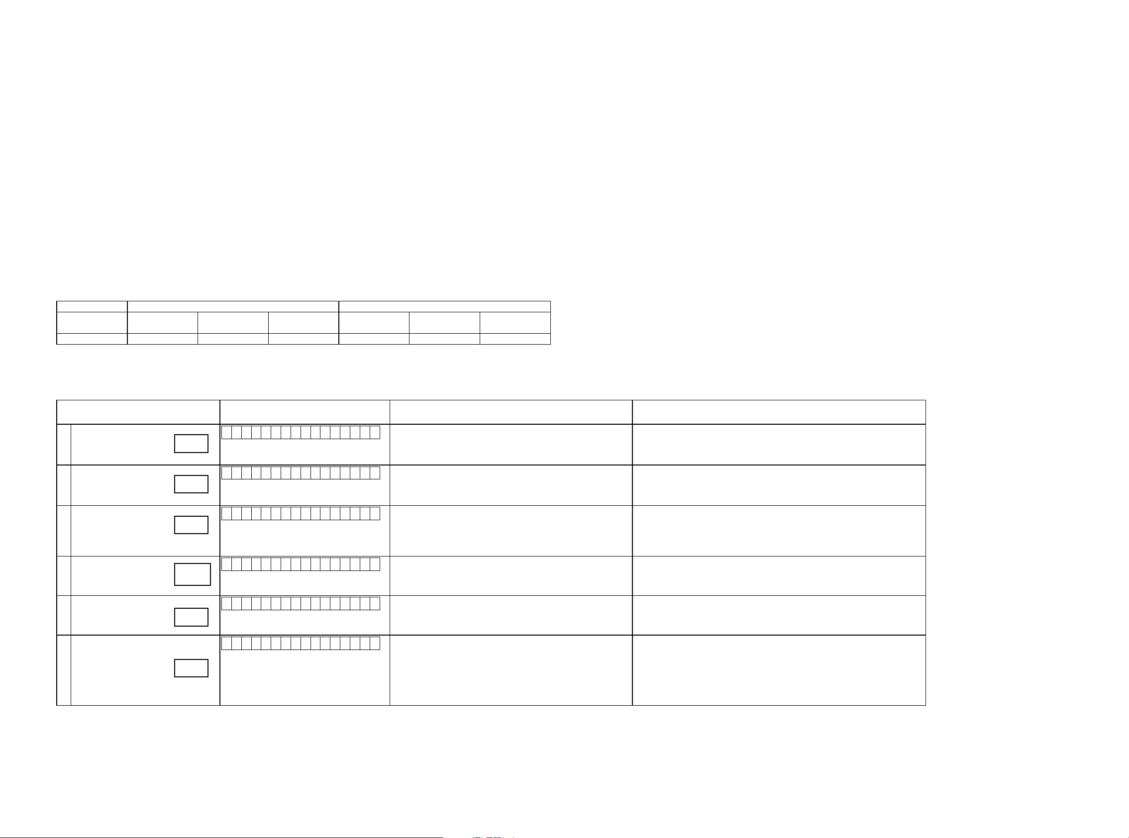
3. Selection Modes for Service-related Operations
3.1. Actions
Select diagnostic mode (service path check mode), protection history display mode, or 232C standby clear mode.
3.2. Starting up
AVR-X1100W
Hold down buttons "
the power.
AVR-S700W
Hold down buttons "
on the power.
Select the mode using the button "
ZONE2 SOURCE
TUNER PRESET CH+
3.3. Displaying and Selecting Each Mode
The information shown on the display changes each time the button "
Press the button "
q
FLD
Service Path Check Mode:
The Video and Audio paths can be checked.
This function is convenient for conrming problem paths in the product and executing a path
check after repair.
w
FLD
The protection history can be checked.
STATUS
" to set the currently displayed mode and restart the device.
1 . S E R V I C E C H E C K
2 . P R O T E C T I O N
DIMMER
", "
TUNER PRESET CH+
", "
" and "
TUNE -
" and
STATUS
", and press the button "
" at the same time and press the power button to turn on
TUNE +
" at the same time and press the power button to turn
TUNER PRESET CH+
STATUS
" to commit the selection.
" is pressed.
e
FLD
Operation Info for the unit can be checked.
r
FLD
Enables reception STEP of the ANALOG TUNER to be changed.
t
FLD
Function to operate only the desired AV receiver.
4 . O P I N F O
5 . T U N E R F R Q S E T
6 . R E M O T E I D
3.3. Canceling the mode
Press the power button to turn off the power.
23
Page 24

Personal notes:
24
Page 25
3.4. DIAGNOSTIC MODE (Service Path Check Mode)
3.4.1. Actions
This function is convenient for conrming problem paths in the product and executing a path check after repair.
The Video and Audio paths can be checked.
The backup data is not rewritten.
3.4.2. Starting up
AVR-X1100W
Hold down buttons "
ZONE2 SOURCE
DIMMER
", "
" and "
STATUS
" at the same time and press the power button to turn on the power.
AVR-S700W
Hold down buttons "
TUNER PRESET CH +
Select the mode using the button "
Select "
The "
1. SERVICE CHECK
TUNED
STERO
", "
" and press the "
RDS
" and "
TUNER PRESET CH+
" segments are lit in this mode.
TUNE -
", "
STATUS
TUNE +
" and "
", and press the button "
" at the same time and press the power button to turn on the power.
STATUS
" button to start the diagnostic mode.
" to commit the selection.
3.4.3. Canceling diagnostic mode
Press the power button to turn off the power.
3.4.4. Selecting items
Press q button to switch between video items and audio items.
Press button w or e to select the previous or next item.
The unit Remote control unit
Actions
Button DIMMER QUICK SELECT 1 QUICK SELECT 2 SLEEP CURSOR LEFT CURSOR RIGHT
q w e q w e
Audio ⇔ Video PREVIOUS NEXT Audio ⇔ Video PREVIOUS NEXT
3.4.5. Video system conrmation items
g. XX: See the block diagram of the g.XXth.
Paths conrmation item Display Settings Contents of conrmation Remarks
Analog Video pass
1
HDMI pass
MAIN ZONE
(
2
HDMI CEC
3
HDMI Audio
(Audio: AVR)
4
HDMI Audio
(Audio: TV)
5
GUI
6
g.01
)
g.02
g.03
g.04a
g.04b
g.05
g.06
V 0 1 : V I D E O P A S S
V 0 3 : H D M I P A S S
V 0 4 : H D M I C E C
V 0 5 : H . A U D I O - A V R
V 0 6 : H . A U D I O - T V
V 0 7 : G U I M E N U O N
Input Source : CBL/SAT
Source of Video Convert(IP Scaler) : OFF, All sources
MAIN ZONE ON
ZONE2 ON
Input Source : CBL/SAT
Source of Video Convert(IP Scaler) : OFF, All sources
MAIN ZONE ON
ZONE2 OFF
Input Source : CBL/SAT
HDMI Control : ON
MAIN ZONE ON
ZONE2 OFF
Input Source : CBL/SAT
HDMI Control : OFF
HDMI Audio:AVR ( if checking the audio output from AVR )
HDMI Audio:TV ( if checking the audio output from TV )
Input Source : CBL/SAT
Video Convert(IP Scaler) : ON, All sources
IP Scaler : "Analog & HDMI", All sources
Resolution : "AUTO", All sources
Setup Menu ON
MAIN ZONE ON
ZONE2 OFF
Check of CVBS input ⇒ CVBS output.
・
The input source can be switched to any source except CBL/SAT.
(※
Check of HDMI input(MAIN Function)⇒HDMI output(MAIN
・
The input source can be switched to any source except CBL/SAT.
(※
When the TV is set to Standby by the HDMI1 OUT, check that this unit switches
・
to Standby
The ARC path can also be checked (check this using the TV input source).
・
The input source can be switched to any source except CBL/SAT.
(※
Check of HDMI input(PCM , DolbyDigital , DTS) ⇒ Speaker output.
・
Check of HDMI input(HD audio) ⇒ Speaker output.
・
The input source can be switched to any source except CBL/SAT.
(※
Check of HDMI input(PCM , DolbyDigital , DTS) ⇒ HDMI output (audio output
・
from connected TV)
The input source can be switched to any source except CBL/SAT.
(※
Check of GUI display ⇒ HDMI output.
・
The input source can be switched to any source except CBL/SAT.
(※
)
)
)
)
)
)
)
25
Page 26
3.4.6. Audio system conrmation items
g. XX: See the block diagram of the g.XXth.
Paths conrmation item Display Settings Contents of conrmation Remarks
Analog ( pass )
1
DIGITAL
(MAIN)
2
HDMI
3
Analog AD
(MAIN)
4
Analog Amp Assign
(Amp Assign: ZONE2)
5
Analog Amp Assign
(Amp Assign: Bi-Amp)
AVR-X1100W Only
6
Front Height
7
g.07
g.08a
g.08b
g.09a
g.09b
g.10a
g.10b
g.11
g.12
g.13a
g.13b
A 0 1 : A N A L O G P A S S
A 0 2 : D I G I T A L
A 0 5 : H D M I
A 0 6 : A D
A 0 7 : A S S I G N - Z 2
A 1 1 : A S S I G N - B i A M P
A 1 4 : F R O N T H E I G H T
Input Source: CBL/SAT
Input Mode: ANALOG xed
Sound mode: DIRECT
Amp assign: Surround Back
MAIN ZONE: ON
ZONE2: OFF
Input Source : CBL/SAT
Input Mode : DIGITAL xed
Sound mode: MULTI CH STEREO
Amp assign : Surround Back
Speaker Cong all Speaker=Small / SW=Yes(2ch)
MAIN ZONE ON
ZONE2 OFF
Input Source : CBL/SAT
Input Mode : HDMI xed
Sound mode: STEREO
Amp assign : Surround Back
MAIN ZONE: ON
ZONE2: OFF
Input Source : CBL/SAT
Input Mode : Analog xed
Sound mode: MULTI CH STEREO
Vol -20dB
Amp assign : Surround Back
Speaker Cong all Speaker=Small / SW=Yes(2ch)
MAIN ZONE: ON
ZONE2: OFF
Input Source : CBL/SAT
Input Mode : Auto
Sound mode: STEREO
Z2 Source : Source
Vol -20dB
Amp assign : ZONE2
MAIN ZONE: ON
ZONE2: ON
Input Source : CBL/SAT
Input Mode : Auto
Sound mode: MULTI CH STEREO
Amp assign : Bi-Amp
MAIN ZONE ON
ZONE2 OFF
Input Source : CBL/SAT
Input Mode : Auto
Sound mode: MULTI CH STEREO
Vol -20dB
Amp assign : Front Height
MAIN ZONE ON
ZONE2 OFF
Check the audio output.
・
Check of Analog input ⇒ Speaker output.
・
Front L/R
The input source can be switched to any source except CBL/SAT.
(※
Check the audio output.
・
Check of Digital input ⇒ Speaker output.
・
Front L/R、 Center、 Surround L/R、Surround Back L/R
Check of Digital(PCM) input ⇒ Preout output.
・
Front L/R、 Center、 Surround L/R、Surround Back L/R、Subwoofer
The input source can be switched to any source except CBL/SAT.
(※
Check the audio output.
・
HDMI input ⇒ Speaker output.
・
Front L/R
The input source can be switched to any source except CBL/SAT.
(※
Check the audio output.
・
Check of Analog input ⇒ Speaker output.
・
Front L/R、 Center、 Surround L/R、Surround Back L/R
Check of Analog input ⇒ Pre OUT.
・
Front L/R、 Center、 Surround L/R、Surround Back L/R、Subwoofer
The input source can be switched to any source except CBL/SAT.
(※
Volume -20dB is the value when Relative settings are used. The value is 60
(※
when Absolute settings are used
Check the audio output.
・
Check of Analog input ⇒ Speaker output.
・
Surround Back(ZONE2) L/R
Check of Analog input ⇒ Pre OUT.
・
ZONE2 L/R
The input source can be switched to any source except CBL/SAT.
(※
Volume -20dB is the value when Relative settings are used. The value is 60
(※
when Absolute settings are used
Check the audio output.
・
Check of Analog input ⇒ Speaker output.
・
Surround Back L/R
The input source can be switched to any source except CBL/SAT.
(※
Volume -20dB is the value when Relative settings are used. The value is 60
(※
when Absolute settings are used
Check the audio output.
・
Check of Analog input ⇒ Speaker output.
・
Surround Back L/R
The input source can be switched to any source except CBL/SAT.
(※
Check of PREOUT output.
・
Volume -20dB is the value when Relative settings are used. The value is 60
(※
when Absolute settings are used
)
)
)
)
)
)
)
)
)
)
)
26
Page 27
DIAGNOSTIC PATH DIAGRAM
fig.01
AVR-S700W/X1100W VIDEO BLOCK
F-HDMI IN
(AUX)
P3 RX
AD8195
Buffer
HDMI RX(MN864778A)
27.000MHz
HDMI IN1
(CBL/SAT)
HDMI IN2
(DVD)
HDMI IN3
(MEDIA Player)
HDMI IN4
(GAME)
HDMI IN5
(Blu-ray)
CY920
P2 RX
P1 RX
P0 RX
CEA 861(V0~V7, PCLKIN)
P1 RX
P0 RX
P1 TX
X7201
28.6363MHz
ADV7623
TRANSCEIVER
OSD Block
OTHER : 32M
E1 : 64M
S.FLASH
32M/64M
P3 RX
P1 RX
P0 RX
HDMI TX(MN8647781)
MAIN
SUB
27.000MHz
P0 TX
P1 TX
HDMI OUT
MONITOR OUT
CVBS IN
Media Player
SAT/CBL
NJM2595
20K
20K
20K
20K
6dB
6dB
6dB
75ohm
Driver
75ohm
Driver
75ohm
Driver
CVBS OUT
MONITOR OUT
27
Page 28
fig.02
F-HDMI IN
(AUX)
AVR-S700W/X1100W VIDEO BLOCK
HDMI RX(MN864778A)
P3 RX
AD8195
Buffer
27.000MHz
HDMI IN1
(CBL/SAT)
HDMI IN2
(DVD)
HDMI IN3
(MEDIA Player)
HDMI IN4
(GAME)
HDMI IN5
(Blu-ray)
CY920
P2 RX
P1 RX
P0 RX
CEA 861(V0~V7, PCLKIN)
P1 RX
P0 RX
P1 TX
X7201
28.6363MHz
ADV7623
TRANSCEIVER
OSD Block
OTHER : 32M
E1 : 64M
S.FLASH
32M/64M
P3 RX
P1 RX
P0 RX
HDMI TX(MN8647781)
MAIN
SUB
27.000MHz
P0 TX
P1 TX
HDMI OUT
MONITOR OUT
CVBS IN
Media Player
SAT/CBL
NJM2595
20K
20K
20K
20K
6dB
6dB
6dB
75ohm
Driver
75ohm
Driver
75ohm
Driver
CVBS OUT
MONITOR OUT
28
Page 29
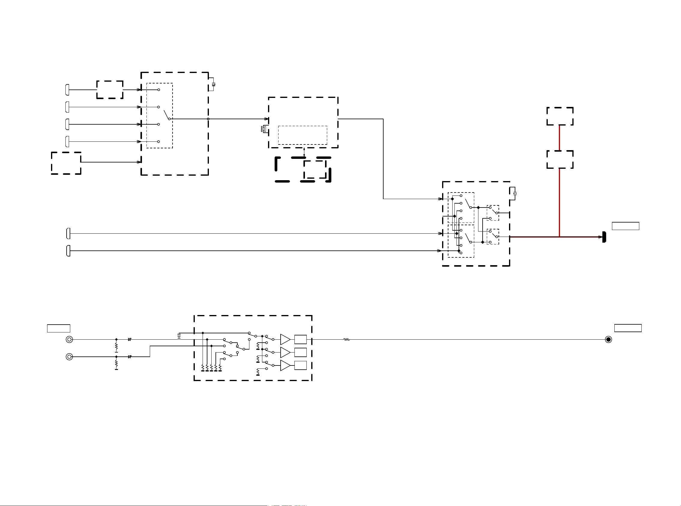
fig.03
F-HDMI IN
(AUX)
AVR-S700W/X1100W VIDEO BLOCK
HDMI RX(MN864778A)
P3 RX
AD8195
Buffer
27.000MHz
HDMI IN1
(CBL/SAT)
HDMI IN2
(DVD)
HDMI IN3
(MEDIA Player)
HDMI IN4
(GAME)
HDMI IN5
(Blu-ray)
CY920
P2 RX
P1 RX
P0 RX
CEA 861(V0~V7, PCLKIN)
P1 RX
P0 RX
P1 TX
X7201
28.6363MHz
ADV7623
TRANSCEIVER
OSD Block
OTHER : 32M
E1 : 64M
S.FLASH
32M/64M
P3 RX
P1 RX
P0 RX
HDMI TX(MN8647781)
MAIN
SUB
27.000MHz
P0 TX
P1 TX
AD8195
Buffer
AD8195
Buffer
HDMI OUT
MONITOR OUT
CVBS IN
Media Player
SAT/CBL
NJM2595
20K
20K
20K
20K
6dB
6dB
6dB
75ohm
Driver
75ohm
Driver
75ohm
Driver
CVBS OUT
MONITOR OUT
29
Page 30
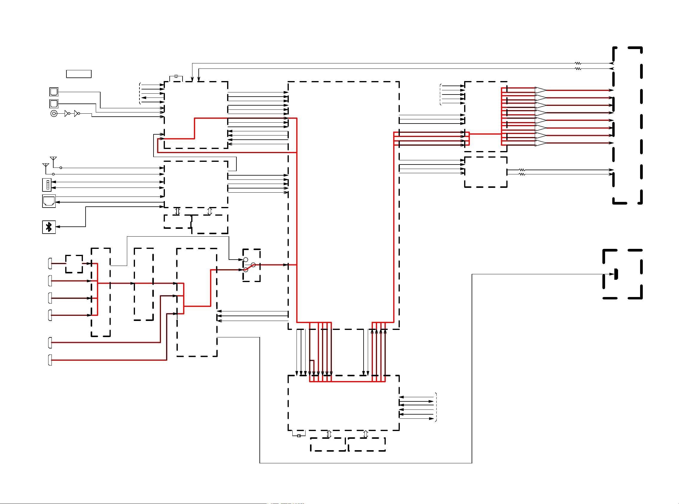
fig.04a
OPT1(TV)
OPT2(CBL/SAT)
COAX1(CBL/SAT)
OTHER : OPT 2 / COAX NONE
E3 : OPT NONE / COAX 1
ANT1
ANT2
USB
ETHERNET
RJ-45 with Transformer
BT MODULE
(ONLY CX870)
DIGTAL IN
USBD-
USBD+
RX+/-
TX+/-
RX/TX/BT_ACTIVE/WLAN_ACTIVE
AVR-S700W/X1100W DIGITAL AUDIO BLOCK
(From/To MCU)
DIR_CE
DIR_CLK
DIR_DIN
DIR_DOUT
DIR_RST
OPT.1
OPT.2
COAX.1
PLD_SPDIF
NET_SPDIF
24.576MHz
CX870(CY920)
NETWORKED MEDIA
IPOD AUTH.
23671011050AS
(MFI337S3959)
ADINL
ADINR
ADC+DIR
PCM9211PTR
MODULE
SERIAL FLASH
256M
MX25L25635FMI-10G
(CY920 ONLY)
NET_SPDIF
MCLK1
256FSDIR1
64FSDIR1
FSDIR1
SBCK
SLRCK
DATADIR1
/AUDIO1
DIR1PERR
RX256FS
RX64FS
RXFS
RXI2SO
PLD_SPDIF
NET_USB_MCK
NET_USB_BCK
NET_USB_LRCK
NET_USBDATAF/FL
NET_USBDATA-/FR
AUDIO PLD
5M80ZT100C5N
DAC256FS
DAC64FS
DACFS
DACDATAF
DACDATAC
DACDATAS
DACDATASB
NET_USB_MCK
NET_USB_BCK
NET_U
NET_USBDATA
(From MCU)
SB_LRCK
DAC_MUTE
DAC_RST
DAC_MS
DAC_DATA
DAC_CLK
DAC
PCM1690
Z2 NETWORK
DAC
PCM5100
ADINL
ADINR
FL
FR
C
SW
SL
SR
SBL
SBR
NET_L
NET_R
ANALOG AUDIO BLOCK
F-HDMI IN
(AUX)
HDMI IN1
(CBL/SAT)
HDMI IN2
(DVD)
HDMI IN3
(MEDIA Player)
HDMI IN4
(GAME)
HDMI IN5
(Blu-ray)
TMDS
TMDS
TMDS
TMDS
TMDS
TMDS
AD8195
Buffer
I2S_DATA/CLK
TMDS TMDS
HDMI RX(MN864778A)
I2S_DATA/CLK
TC74VHC157FT X 2
I2S_DATA/CLK
HDMI OUT
ADV7623
TX64FS
TXFS
TXI2S0
HDMI TX(MN8647781)
TMDS
DATAF
DATAC
DATAS
DSP1INMCK
DSP1IN64FS
DSP1INFS
DSP1INSB/SR
DSP1INF/FL
DSP1INCSW/C
DSP1IN-/FR
DSP1INS/SL
DSP
ADSP21487KSWZ-3B
350MHz
DSP1OUT64FS
DATASB
DSP1OUTFS
DSP_MOSI
DSP_MISO
DSP_CLK
DSP_RST
DSP_CS
DSP_FLAG0
(From / To MCU)
21.875MHz
W9864G6JH-6
30
SERIAL FLASHSDRAM
16M64M
MX25L1606EM2I-12G
Page 31

fig.04b
AVR-S700W/X1100W ANALOG AUDIO BLOCK
ANA01
DA01
ANA02
DA02
ANA01
MAIN
TUNER
FM/AM
32.768kHz
DA03
ANA_FL
DA_FL
ANA_FR
DA_FR
DA_CEN
P-AMP
H/P OUT
H/P L
GND
H/P R
SPK OUT
+
FL
-
+
FR
-
+
CEN
-
AUDIO IN
Media Player
CBL/SAT
AUDYSSEY
MIC(AUTO SETUP)
AVR-X1100W E3 ONLY
TO DIGITAL
AUDIO BLOCK
ZONE2
AD_FL
AD_FR
DA_FL
DA_FR
DA_CEN
DA_SW
DA_SL
DA_SR
DA_SBL
DA_SBR
NETWORK
MUTE
VOL IC
BD3812F
DA01
DA02
DA03
DA04
DA05
DA06
DA07
DA08
DA04
DA05
DA06
DA07
DA08
DA_SW
DA_SL
DA_SR
DA_SBL
DA_SBR
VOL IC
NJU72340A
MUTE
+
SL
-
+
SR
-
+
SBL
-
(FL-H/FL-B/BI-AMP-FL/ZONE-FL)
+
SBR
-
(FR-H/FR-B/BI-AMP-FR/ZONE-FR)
PRE OUT
SW1
SW2
31
Page 32

fig.05
OPT1(TV)
OPT2(CBL/SAT)
COAX1(CBL/SAT)
OTHER : OPT 2 / COAX NONE
E3 : OPT NONE / COAX 1
ANT1
ANT2
USB
ETHERNET
RJ-45 with Transformer
BT MODULE
(ONLY CX870)
DIGTAL IN
USBD-
USBD+
RX+/-
TX+/-
RX/TX/BT_ACTIVE/WLAN_ACTIVE
AVR-S700W/X1100W DIGITAL AUDIO BLOCK
(From/To MCU)
DIR_CE
DIR_CLK
DIR_DIN
DIR_DOUT
DIR_RST
OPT.1
OPT.2
COAX.1
PLD_SPDIF
NET_SPDIF
24.576MHz
CX870(CY920)
NETWORKED MEDIA
IPOD AUTH.
23671011050AS
(MFI337S3959)
ADINL
ADINR
ADC+DIR
PCM9211PTR
MODULE
SERIAL FLASH
256M
MX25L25635FMI-10G
(CY920 ONLY)
NET_SPDIF
MCLK1
256FSDIR1
64FSDIR1
FSDIR1
SBCK
SLRCK
DATADIR1
/AUDIO1
DIR1PERR
RX256FS
RX64FS
RXFS
RXI2SO
PLD_SPDIF
NET_USB_MCK
NET_USB_BCK
NET_USB_LRCK
NET_USBDATAF/FL
NET_USBDATA-/FR
AUDIO PLD
5M80ZT100C5N
DAC256FS
DAC64FS
DACFS
DACDATAF
DACDATAC
DACDATAS
DACDATASB
NET_USB_MCK
NET_USB_BCK
NET_U
NET_USBDATA
(From MCU)
SB_LRCK
DAC_MUTE
DAC_RST
DAC_MS
DAC_DATA
DAC_CLK
DAC
PCM1690
Z2 NETWORK
DAC
PCM5100
ADINL
ADINR
FL
FR
C
SW
SL
SR
SBL
SBR
NET_L
NET_R
ANALOG AUDIO BLOCK
F-HDMI IN
(AUX)
HDMI IN1
(CBL/SAT)
HDMI IN2
(DVD)
HDMI IN3
(MEDIA Player)
HDMI IN4
(GAME)
HDMI IN5
(Blu-ray)
TMDS
TMDS
TMDS
TMDS
TMDS
TMDS
AD8195
Buffer
I2S_DATA/CLK
TMDS TMDS
HDMI RX(MN864778A)
I2S_DATA/CLK
TC74VHC157FT X 2
I2S_DATA/CLK
HDMI OUT
ADV7623
TX64FS
TXFS
TXI2S0
HDMI TX(MN8647781)
TMDS
DATAF
DATAC
DATAS
DSP1INMCK
DSP1IN64FS
DSP1INFS
DSP1INSB/SR
DSP1INF/FL
DSP1INCSW/C
DSP1IN-/FR
DSP1INS/SL
DSP
ADSP21487KSWZ-3B
350MHz
DSP1OUT64FS
DATASB
DSP1OUTFS
DSP_MOSI
DSP_MISO
DSP_CLK
DSP_RST
DSP_CS
DSP_FLAG0
(From / To MCU)
21.875MHz
W9864G6JH-6
32
SERIAL FLASHSDRAM
16M64M
MX25L1606EM2I-12G
Page 33

fig.06
F-HDMI IN
(AUX)
AVR-S700W/X1100W VIDEO BLOCK
HDMI RX(MN864778A)
P3 RX
AD8195
Buffer
27.000MHz
HDMI IN1
(CBL/SAT)
HDMI IN2
(DVD)
HDMI IN3
(MEDIA Player)
HDMI IN4
(GAME)
HDMI IN5
(Blu-ray)
CY920
P2 RX
P1 RX
P0 RX
CEA 861(V0~V7, PCLKIN)
P1 RX
P0 RX
P1 TX
X7201
28.6363MHz
ADV7623
TRANSCEIVER
OSD Block
OTHER : 32M
E1 : 64M
S.FLASH
32M/64M
P3 RX
P1 RX
P0 RX
HDMI TX(MN8647781)
MAIN
SUB
27.000MHz
P0 TX
P1 TX
HDMI OUT
MONITOR OUT
CVBS IN
Media Player
SAT/CBL
NJM2595
20K
20K
20K
20K
6dB
6dB
6dB
75ohm
Driver
75ohm
Driver
75ohm
Driver
CVBS OUT
MONITOR OUT
33
Page 34

fig.07
AVR-S700W/X1100W ANALOG AUDIO BLOCK
ANA01
DA01
ANA02
DA02
ANA01
MAIN
TUNER
FM/AM
32.768kHz
DA03
ANA_FL
DA_FL
ANA_FR
DA_FR
DA_CEN
P-AMP
H/P OUT
H/P L
GND
H/P R
SPK OUT
+
FL
-
+
FR
-
+
CEN
-
AUDIO IN
Media Player
CBL/SAT
AUDYSSEY
MIC(AUTO SETUP)
AVR-X1100W E3 ONLY
TO DIGITAL
AUDIO BLOCK
ZONE2
AD_FL
AD_FR
DA_FL
DA_FR
DA_CEN
DA_SW
DA_SL
DA_SR
DA_SBL
DA_SBR
NETWORK
MUTE
VOL IC
BD3812F
DA01
DA02
DA03
DA04
DA05
DA06
DA07
DA08
DA04
DA05
DA06
DA07
DA08
DA_SW
DA_SL
DA_SR
DA_SBL
DA_SBR
VOL IC
NJU72340A
MUTE
+
SL
-
+
SR
-
+
SBL
-
(FL-H/FL-B/BI-AMP-FL/ZONE-FL)
+
SBR
-
(FR-H/FR-B/BI-AMP-FR/ZONE-FR)
PRE OUT
SW1
SW2
34
Page 35

fig.08a
OPT1(TV)
OPT2(CBL/SAT)
COAX1(CBL/SAT)
OTHER : OPT 2 / COAX NONE
E3 : OPT NONE / COAX 1
ANT1
ANT2
USB
ETHERNET
RJ-45 with Transformer
BT MODULE
(ONLY CX870)
DIGTAL IN
USBD-
USBD+
RX+/-
TX+/-
RX/TX/BT_ACTIVE/WLAN_ACTIVE
AVR-S700W/X1100W DIGITAL AUDIO BLOCK
(From/To MCU)
DIR_CE
DIR_CLK
DIR_DIN
DIR_DOUT
DIR_RST
OPT.1
OPT.2
COAX.1
NET_SPDIF
24.576MHz
PLD_SPDIF
CX870(CY920)
NETWORKED MEDIA
IPOD AUTH.
23671011050AS
(MFI337S3959)
ADINL
ADINR
ADC+DIR
PCM9211PTR
MODULE
SERIAL FLASH
256M
MX25L25635FMI-10G
(CY920 ONLY)
NET_SPDIF
MCLK1
256FSDIR1
64FSDIR1
FSDIR1
SBCK
SLRCK
DATADIR1
/AUDIO1
DIR1PERR
RX256FS
RX64FS
RXFS
RXI2SO
PLD_SPDIF
NET_USB_MCK
NET_USB_BCK
NET_USB_LRCK
NET_USBDATAF/FL
NET_USBDATA-/FR
AUDIO PLD
5M80ZT100C5N
DAC256FS
DAC64FS
DACFS
DACDATAF
DACDATAC
DACDATAS
DACDATASB
NET_USB_MCK
NET_USB_BCK
NET_U
NET_USBDATA
(From MCU)
SB_LRCK
DAC_MUTE
DAC_RST
DAC_MS
DAC_DATA
DAC_CLK
DAC
PCM1690
Z2 NETWORK
DAC
PCM5100
ADINL
ADINR
FL
FR
C
SW
SL
SR
SBL
SBR
NET_L
NET_R
ANALOG AUDIO BLOCK
F-HDMI IN
(AUX)
HDMI IN1
(CBL/SAT)
HDMI IN2
(DVD)
HDMI IN3
(MEDIA Player)
HDMI IN4
(GAME)
HDMI IN5
(Blu-ray)
TMDS
TMDS
TMDS
TMDS
TMDS
TMDS
AD8195
Buffer
I2S_DATA/CLK
TMDS TMDS
HDMI RX(MN864778A)
I2S_DATA/CLK
TC74VHC157FT X 2
I2S_DATA/CLK
HDMI OUT
ADV7623
TX64FS
TXFS
TXI2S0
HDMI TX(MN8647781)
TMDS
DATAF
DATAC
DATAS
DSP1INMCK
DSP1IN64FS
DSP1INFS
DSP1INSB/SR
DSP1INF/FL
DSP1INCSW/C
DSP1IN-/FR
DSP1INS/SL
DSP
ADSP21487KSWZ-3B
350MHz
DSP1OUT64FS
DATASB
DSP1OUTFS
DSP_MOSI
DSP_MISO
DSP_CLK
DSP_RST
DSP_CS
DSP_FLAG0
(From / To MCU)
21.875MHz
W9864G6JH-6
35
SERIAL FLASHSDRAM
16M64M
MX25L1606EM2I-12G
Page 36

fig.08b
AVR-S700W/X1100W ANALOG AUDIO BLOCK
ANA01
DA01
ANA02
DA02
ANA01
MAIN
TUNER
FM/AM
32.768kHz
DA03
ANA_FL
DA_FL
ANA_FR
DA_FR
DA_CEN
P-AMP
H/P OUT
H/P L
GND
H/P R
SPK OUT
+
FL
-
+
FR
-
+
CEN
-
AUDIO IN
Media Player
AUDYSSEY
MIC(AUTO SETUP)
AVR-X1100W E3 ONLY
TO DIGITAL
AUDIO BLOCK
CBL/SAT
ZONE2
NETWORK
AD_FL
AD_FR
DA_FL
DA_FR
DA_CEN
DA_SW
DA_SL
DA_SR
DA_SBL
DA_SBR
MUTE
VOL IC
BD3812F
DA01
DA02
DA03
DA04
DA05
DA06
DA07
DA08
DA04
DA05
DA06
DA07
DA08
DA_SW
DA_SL
DA_SR
DA_SBL
DA_SBR
VOL IC
NJU72340A
MUTE
+
SL
-
+
SR
-
+
SBL
-
(FL-H/FL-B/BI-AMP-FL/ZONE-FL)
+
SBR
-
(FR-H/FR-B/BI-AMP-FR/ZONE-FR)
PRE OUT
SW1
SW2
36
Page 37

fig.09a
OPT1(TV)
OPT2(CBL/SAT)
COAX1(CBL/SAT)
OTHER : OPT 2 / COAX NONE
E3 : OPT NONE / COAX 1
ANT1
ANT2
USB
ETHERNET
RJ-45 with Transformer
BT MODULE
(ONLY CX870)
DIGTAL IN
USBD-
USBD+
RX+/-
TX+/-
RX/TX/BT_ACTIVE/WLAN_ACTIVE
AVR-S700W/X1100W DIGITAL AUDIO BLOCK
(From/To MCU)
DIR_CE
DIR_CLK
DIR_DIN
DIR_DOUT
DIR_RST
OPT.1
OPT.2
COAX.1
NET_SPDIF
24.576MHz
PLD_SPDIF
CX870(CY920)
NETWORKED MEDIA
IPOD AUTH.
23671011050AS
(MFI337S3959)
ADINL
ADINR
ADC+DIR
PCM9211PTR
MODULE
SERIAL FLASH
256M
MX25L25635FMI-10G
(CY920 ONLY)
NET_SPDIF
MCLK1
256FSDIR1
64FSDIR1
FSDIR1
SBCK
SLRCK
DATADIR1
/AUDIO1
DIR1PERR
RX256FS
RX64FS
RXFS
RXI2SO
PLD_SPDIF
NET_USB_MCK
NET_USB_BCK
NET_USB_LRCK
NET_USBDATAF/FL
NET_USBDATA-/FR
AUDIO PLD
5M80ZT100C5N
DAC256FS
DAC64FS
DACFS
DACDATAF
DACDATAC
DACDATAS
DACDATASB
NET_USB_MCK
NET_USB_BCK
NET_U
NET_USBDATA
(From MCU)
SB_LRCK
DAC_MUTE
DAC_RST
DAC_MS
DAC_DATA
DAC_CLK
DAC
PCM1690
Z2 NETWORK
DAC
PCM5100
ADINL
ADINR
FL
FR
C
SW
SL
SR
SBL
SBR
NET_L
NET_R
ANALOG AUDIO BLOCK
F-HDMI IN
(AUX)
HDMI IN1
(CBL/SAT)
HDMI IN2
(DVD)
HDMI IN3
(MEDIA Player)
HDMI IN4
(GAME)
HDMI IN5
(Blu-ray)
TMDS
TMDS
TMDS
TMDS
TMDS
TMDS
AD8195
Buffer
I2S_DATA/CLK
TMDS TMDS
HDMI RX(MN864778A)
I2S_DATA/CLK
TC74VHC157FT X 2
I2S_DATA/CLK
HDMI OUT
ADV7623
TX64FS
TXFS
TXI2S0
HDMI TX(MN8647781)
TMDS
DATAF
DATAC
DATAS
DSP1INMCK
DSP1IN64FS
DSP1INFS
DSP1INSB/SR
DSP1INF/FL
DSP1INCSW/C
DSP1IN-/FR
DSP1INS/SL
DSP
ADSP21487KSWZ-3B
350MHz
DSP1OUT64FS
DATASB
DSP1OUTFS
DSP_MOSI
DSP_MISO
DSP_CLK
DSP_RST
DSP_CS
DSP_FLAG0
(From / To MCU)
21.875MHz
W9864G6JH-6
37
SERIAL FLASHSDRAM
16M64M
MX25L1606EM2I-12G
Page 38

fig.09b
AVR-S700W/X1100W ANALOG AUDIO BLOCK
ANA01
DA01
ANA02
DA02
ANA01
MAIN
TUNER
FM/AM
32.768kHz
DA03
ANA_FL
DA_FL
ANA_FR
DA_FR
DA_CEN
P-AMP
H/P OUT
H/P L
GND
H/P R
SPK OUT
+
FL
-
+
FR
-
+
CEN
-
AUDIO IN
Media Player
CBL/SAT
AUDYSSEY
MIC(AUTO SETUP)
AVR-X1100W E3 ONLY
TO DIGITAL
AUDIO BLOCK
ZONE2
AD_FL
AD_FR
DA_FL
DA_FL
DA_FR
DA_CEN
DA_SW
DA_SL
DA_SR
DA_SBL
DA_SBR
NETWORK
MUTE
VOL IC
BD3812F
DA01
DA02
DA03
DA04
DA05
DA06
DA07
DA08
DA04
DA05
DA06
DA07
DA08
DA_SW
DA_SL
DA_SR
DA_SBL
DA_SBR
VOL IC
NJU72340A
MUTE
+
SL
-
+
SR
-
+
SBL
-
(FL-H/FL-B/BI-AMP-FL/ZONE-FL)
+
SBR
-
(FR-H/FR-B/BI-AMP-FR/ZONE-FR)
PRE OUT
SW1
SW2
38
Page 39

fig.10a
OPT1(TV)
OPT2(CBL/SAT)
COAX1(CBL/SAT)
OTHER : OPT 2 / COAX NONE
E3 : OPT NONE / COAX 1
ANT1
ANT2
USB
ETHERNET
RJ-45 with Transformer
BT MODULE
(ONLY CX870)
DIGTAL IN
USBD-
USBD+
RX+/-
TX+/-
RX/TX/BT_ACTIVE/WLAN_ACTIVE
AVR-S700W/X1100W DIGITAL AUDIO BLOCK
(From/To MCU)
DIR_CE
DIR_CLK
DIR_DIN
DIR_DOUT
DIR_RST
OPT.1
OPT.2
COAX.1
NET_SPDIF
24.576MHz
PLD_SPDIF
CX870(CY920)
NETWORKED MEDIA
IPOD AUTH.
23671011050AS
(MFI337S3959)
ADINL
ADINR
ADC+DIR
PCM9211PTR
MODULE
SERIAL FLASH
256M
MX25L25635FMI-10G
(CY920 ONLY)
NET_SPDIF
MCLK1
256FSDIR1
64FSDIR1
FSDIR1
SBCK
SLRCK
DATADIR1
/AUDIO1
DIR1PERR
RX256FS
RX64FS
RXFS
RXI2SO
PLD_SPDIF
NET_USB_MCK
NET_USB_BCK
NET_USB_LRCK
NET_USBDATAF/FL
NET_USBDATA-/FR
AUDIO PLD
5M80ZT100C5N
DAC256FS
DAC64FS
DACFS
DACDATAF
DACDATAC
DACDATAS
DACDATASB
NET_USB_MCK
NET_USB_BCK
NET_U
NET_USBDATA
(From MCU)
SB_LRCK
DAC_MUTE
DAC_RST
DAC_MS
DAC_DATA
DAC_CLK
DAC
PCM1690
Z2 NETWORK
DAC
PCM5100
ADINL
ADINR
FL
FR
C
SW
SL
SR
SBL
SBR
NET_L
NET_R
ANALOG AUDIO BLOCK
F-HDMI IN
(AUX)
HDMI IN1
(CBL/SAT)
HDMI IN2
(DVD)
HDMI IN3
(MEDIA Player)
HDMI IN4
(GAME)
HDMI IN5
(Blu-ray)
TMDS
TMDS
TMDS
TMDS
TMDS
TMDS
AD8195
Buffer
I2S_DATA/CLK
TMDS TMDS
HDMI RX(MN864778A)
I2S_DATA/CLK
TC74VHC157FT X 2
I2S_DATA/CLK
HDMI OUT
ADV7623
TX64FS
TXFS
TXI2S0
HDMI TX(MN8647781)
TMDS
DATAF
DATAC
DATAS
DSP1INMCK
DSP1IN64FS
DSP1INFS
DSP1INSB/SR
DSP1INF/FL
DSP1INCSW/C
DSP1IN-/FR
DSP1INS/SL
DSP
ADSP21487KSWZ-3B
350MHz
DSP1OUT64FS
DATASB
DSP1OUTFS
DSP_MOSI
DSP_MISO
DSP_CLK
DSP_RST
DSP_CS
DSP_FLAG0
(From / To MCU)
21.875MHz
W9864G6JH-6
39
SERIAL FLASHSDRAM
16M64M
MX25L1606EM2I-12G
Page 40

fig.10b
AVR-S700W/X1100W ANALOG AUDIO BLOCK
ANA01
DA01
ANA02
DA02
ANA01
MAIN
TUNER
FM/AM
32.768kHz
DA03
ANA_FL
DA_FL
ANA_FR
DA_FR
DA_CEN
P-AMP
H/P OUT
H/P L
GND
H/P R
SPK OUT
+
FL
-
+
FR
-
+
CEN
-
AUDIO IN
Media Player
CBL/SAT
AUDYSSEY
MIC(AUTO SETUP)
AVR-X1100W E3 ONLY
TO DIGITAL
AUDIO BLOCK
ZONE2
AD_FL
AD_FR
DA_FL
DA_FR
DA_CEN
DA_SW
DA_SL
DA_SR
DA_SBL
DA_SBR
NETWORK
MUTE
VOL IC
BD3812F
DA01
DA02
DA03
DA04
DA05
DA06
DA07
DA08
DA04
DA05
DA06
DA07
DA08
DA_SW
DA_SL
DA_SR
DA_SBL
DA_SBR
VOL IC
NJU72340A
MUTE
+
SL
-
+
SR
-
+
SBL
-
(FL-H/FL-B/BI-AMP-FL/ZONE-FL)
+
SBR
-
(FR-H/FR-B/BI-AMP-FR/ZONE-FR)
PRE OUT
SW1
SW2
40
Page 41

fig.11
AVR-S700W/X1100W ANALOG AUDIO BLOCK
ANA01
DA01
ANA02
DA02
ANA01
MAIN
TUNER
FM/AM
32.768kHz
DA03
ANA_FL
DA_FL
ANA_FR
DA_FR
DA_CEN
P-AMP
H/P OUT
H/P L
GND
H/P R
SPK OUT
+
FL
-
+
FR
-
+
CEN
-
AUDIO IN
Media Player
CBL/SAT
AUDYSSEY
MIC(AUTO SETUP)
AVR-X1100W E3 ONLY
TO DIGITAL
AUDIO BLOCK
ZONE2
AD_FL
AD_FR
DA_FL
DA_FR
DA_CEN
DA_SW
DA_SL
DA_SR
DA_SBL
DA_SBR
NETWORK
MUTE
VOL IC
BD3812F
DA01
DA02
DA03
DA04
DA05
DA06
DA07
DA08
DA04
DA05
DA06
DA07
DA08
DA_SW
DA_SL
DA_SR
DA_SBL
DA_SBR
VOL IC
NJU72340A
MUTE
+
SL
-
+
SR
-
+
SBL
-
(FL-H/FL-B/BI-AMP-FL/ZONE-FL)
+
SBR
-
(FR-H/FR-B/BI-AMP-FR/ZONE-FR)
PRE OUT
SW1
SW2
41
Page 42

fig.12
AVR-S700W/X1100W ANALOG AUDIO BLOCK
ANA01
DA01
ANA02
DA02
ANA01
MAIN
TUNER
FM/AM
32.768kHz
DA03
ANA_FL
DA_FL
ANA_FR
DA_FR
DA_CEN
P-AMP
H/P OUT
H/P L
GND
H/P R
SPK OUT
+
FL
-
+
FR
-
+
CEN
-
AUDIO IN
Media Player
AUDYSSEY
MIC(AUTO SETUP)
AVR-X1100W E3 ONLY
TO DIGITAL
AUDIO BLOCK
CBL/SAT
ZONE2
NETWORK
AD_FL
AD_FR
DA_FL
DA_FR
DA_CEN
DA_SW
DA_SL
DA_SR
DA_SBL
DA_SBR
MUTE
VOL IC
BD3812F
DA01
DA02
DA03
DA04
DA05
DA06
DA07
DA08
DA04
DA05
DA06
DA07
DA08
DA_SW
DA_SL
DA_SR
DA_SBL
DA_SBR
VOL IC
NJU72340A
MUTE
+
SL
-
+
SR
-
+
SBL
-
(FL-H/FL-B/BI-AMP-FL/ZONE-FL)
+
SBR
-
(FR-H/FR-B/BI-AMP-FR/ZONE-FR)
PRE OUT
SW1
SW2
42
Page 43

fig.13a
OPT1(TV)
OPT2(CBL/SAT)
COAX1(CBL/SAT)
OTHER : OPT 2 / COAX NONE
E3 : OPT NONE / COAX 1
ANT1
ANT2
USB
ETHERNET
RJ-45 with Transformer
BT MODULE
(ONLY CX870)
DIGTAL IN
USBD-
USBD+
RX+/-
TX+/-
RX/TX/BT_ACTIVE/WLAN_ACTIVE
AVR-S700W/X1100W DIGITAL AUDIO BLOCK
(From/To MCU)
DIR_CE
DIR_CLK
DIR_DIN
DIR_DOUT
DIR_RST
OPT.1
OPT.2
COAX.1
NET_SPDIF
24.576MHz
PLD_SPDIF
CX870(CY920)
NETWORKED MEDIA
IPOD AUTH.
23671011050AS
(MFI337S3959)
ADINL
ADINR
ADC+DIR
PCM9211PTR
MODULE
SERIAL FLASH
256M
MX25L25635FMI-10G
(CY920 ONLY)
NET_SPDIF
MCLK1
256FSDIR1
64FSDIR1
FSDIR1
SBCK
SLRCK
DATADIR1
/AUDIO1
DIR1PERR
RX256FS
RX64FS
RXFS
RXI2SO
PLD_SPDIF
NET_USB_MCK
NET_USB_BCK
NET_USB_LRCK
NET_USBDATAF/FL
NET_USBDATA-/FR
AUDIO PLD
5M80ZT100C5N
DAC256FS
DAC64FS
DACFS
DACDATAF
DACDATAC
DACDATAS
DACDATASB
NET_USB_MCK
NET_USB_BCK
NET_U
NET_USBDATA
(From MCU)
SB_LRCK
DAC_MUTE
DAC_RST
DAC_MS
DAC_DATA
DAC_CLK
DAC
PCM1690
Z2 NETWORK
DAC
PCM5100
ADINL
ADINR
FL
FR
C
SW
SL
SR
SBL
SBR
NET_L
NET_R
ANALOG AUDIO BLOCK
F-HDMI IN
(AUX)
HDMI IN1
(CBL/SAT)
HDMI IN2
(DVD)
HDMI IN3
(MEDIA Player)
HDMI IN4
(GAME)
HDMI IN5
(Blu-ray)
TMDS
TMDS
TMDS
TMDS
TMDS
TMDS
AD8195
Buffer
I2S_DATA/CLK
TMDS TMDS
HDMI RX(MN864778A)
I2S_DATA/CLK
TC74VHC157FT X 2
I2S_DATA/CLK
HDMI OUT
ADV7623
TX64FS
TXFS
TXI2S0
HDMI TX(MN8647781)
TMDS
DATAF
DATAC
DATAS
DSP1INMCK
DSP1IN64FS
DSP1INFS
DSP1INSB/SR
DSP1INF/FL
DSP1INCSW/C
DSP1IN-/FR
DSP1INS/SL
DSP
ADSP21487KSWZ-3B
350MHz
DSP1OUT64FS
DATASB
DSP1OUTFS
DSP_MOSI
DSP_MISO
DSP_CLK
DSP_RST
DSP_CS
DSP_FLAG0
(From / To MCU)
21.875MHz
W9864G6JH-6
43
SERIAL FLASHSDRAM
16M64M
MX25L1606EM2I-12G
Page 44

fig.13b
AVR-S700W/X1100W ANALOG AUDIO BLOCK
ANA01
DA01
ANA02
DA02
ANA01
MAIN
TUNER
FM/AM
32.768kHz
DA03
ANA_FL
DA_FL
ANA_FR
DA_FR
DA_CEN
P-AMP
H/P OUT
H/P L
GND
H/P R
SPK OUT
+
FL
-
+
FR
-
+
CEN
-
AUDIO IN
Media Player
AUDYSSEY
MIC(AUTO SETUP)
AVR-X1100W E3 ONLY
TO DIGITAL
AUDIO BLOCK
CBL/SAT
ZONE2
NETWORK
AD_FL
AD_FR
DA_FL
DA_FR
DA_CEN
DA_SW
DA_SL
DA_SR
DA_SBL
DA_SBR
MUTE
VOL IC
BD3812F
DA01
DA02
DA03
DA04
DA05
DA06
DA07
DA08
DA04
DA05
DA06
DA07
DA08
DA_SW
DA_SL
DA_SR
DA_SBL
DA_SBR
VOL IC
NJU72340A
MUTE
+
SL
-
+
SR
-
+
SBL
-
(FL-H/FL-B/BI-AMP-FL/ZONE-FL)
+
SBR
-
(FR-H/FR-B/BI-AMP-FR/ZONE-FR)
PRE OUT
SW1
SW2
44
Page 45

3.5. Protection History Display Mode
3.5.1. Actions
This mode records and displays an event in which the THERMAL, ASO or DC protection was activated.
If protections have been activated multiple times, the latest protection operation is recorded.
3.5.2. Starting up
AVR-X1100W
Hold down buttons "
・
on the power.
AVR-S700W
Hold down buttons "
・
turn on the power.
Select the "
selection.
2. PROTECTION
ZONE2 SOURCE
TUNER PRESET CH+
" using the button "
DIMMER
", "
STATUS
" and "
TUNE -
", "
TUNER PRESET CH+ / -
" and "
PRESET +
" at the same time and press the power button to turn
" at the same time and press the power button to
", and press the button "
STATUS
3.5.3. Protection information and displays
Press the "
・
The protection history can be checked.
・
(1) If no protections have occurred.
FLD
(2) ASO / DC (if the last protection was ASO / DC)
FLD
Cause:
Note:
STATUS
" button in Protection History Display Mode.
N O P R O T E C T
P R T : A S O / D C
A short circuit occurred between the speaker terminals, or speakers with an impedance outside the rating were
connected.
Abnormal DC output from the power amp.
Short circuits in speaker terminals or speakers can be identied.
" to commit the
If the power is turned on during this abnormality, protection is activated after around 6 seconds and the power is turned off.
(4) THERMAL (if the last protection was THERMAL(A) or THERMAL(B))
FLD
P R T : T H E R M A L A
FLD
P R T : T H E R M A L B
Abnormal heat sink temperature.
Cause:
If the power is turned on during this abnormality, protection is activated after around 2 minutes and the power is turned off.
(4) Case of CURRENT (when the last protection incident was CURRENT protection)
FLD
: C U R R E N T
Caution:
around the microcomputer.
After viewing the above protection history, press the button "
These protections may also be activated due to causes such as disconnection of connectors or operations
STATUS
" to return to the normal display.
45
Page 46

3.5.4. Clearing the Protection History
There are two ways to clear the protection history.
(1) Start Protection History Display Mode. Press the button "
button "
FLD
Press and hold the button "
FLD
The above is displayed and the protection history is cleared.
FLD
(2) Initialize this unit. ( "See "
Use the method in
b
DIMMER
" for 3 seconds.
P R T : D C
P R T : C L E A R
N O P R O T E C T
Initializing This Unit
3.5.3.(1)
if you do not want to erase your settings from this unit.
DIMMER
" 11 page )
STATUS
" to display the protection history. Press and hold the
" for 3 seconds.
Warning Displays by POWER LED
If the power is turned off while a protection is detected, the POWER LED (red) ashes in the following ways as a warning
according to the protection status.
(1) ASO/DC protection: Flashes in 0.5-second cycles (0.25 seconds lit, 0.25 seconds unlit)
(2) THERMAL (A/B) protection: Flashes in 2-second cycles (1 second lit, 1 second unlit)
46
Page 47

3.6. Operation Info Mode
3.6.1. Actions
This mode displays the accumulated operating time, power on count and each protection count.
3.6.2. Starting up
AVR-X1100W
Hold down buttons "
・
on the power.
AVR-S700W
Hold down buttons "
・
turn on the power.
Select the "
tion.
4. OP INFO
ZONE2 SOURCE
TUNER PRESET CH+
" using the button "
DIMMER
", "
TUNE -
", "
TUNER PRESET CH+ / -
" and "
" and "
STATUS
" at the same time and press the power button to turn
PRESET +
" at the same time and press the power button to
", and press the button "
STATUS
3.6.3. Operations
Press the "
The following information is displayed in the following order.
(a) Accumulated operating time
FLD
↑Time display
"
STATUS
" button after starting this device in Operation Info mode.
O P T i m e H
STATUS
"
" to commit the selec-
(b) Power on count
FLD
P . O n T i m e
↑Count display
"
(c) DC / ASO Protection count
FLD
D C : / A S O :
"
(d) Thermal Protection count
FLD
T H M A : / B :
"
(e) Thermal Protection count
FLD
C u r r e n t :
"
(Returns to normal display)
STATUS
STATUS
STATUS
STATUS
"
"
"
"
47
Page 48

3.7. TUNER STEP mode (for E2 / E3)
3.3.1. Actions
This is a special mode for enabling reception STEP of the ANALOG TUNER to be changed.
3.7.2. Starting up
AVR-X1100W
Hold down buttons "
・
on the power.
AVR-S700W
Hold down buttons "
・
turn on the power.
Select the "
the selection.
5. TUNER FRQ SER
ZONE2 SOURCE
TUNER PRESET CH+
" using the button "
DIMMER
", "
STATUS
" and "
TUNE -
", "
" and "
TUNER PRESET CH+ / -
" at the same time and press the power button to turn
PRESET +
" at the same time and press the power button to
", and press the button "
3.7.3. Displays
Start this unit in TUNER STEP mode, select using button "
The following information is displayed in the following order.
(a) AM9kHz/FM50kHz selected
FLD
"
< A M 9 / F M 5 0 >
TUNER PRESET CH+
" "
TUNER PRESET CH-
TUNER PRESET CH+/-" and enter using button "
"
STATUS
" to commit
STATUS".
(b) AM10KHz/FM200kHz selected
FLD
"
(C) Press the power button to turn off the power.
(D) Press the power button to turn on the power.
< A M 1 0 / F M 2 0 0 >
STATUS
"
48
Page 49

4. Remote ID Setup Mode
4.1. Actions
This function allows only the desired AV receiver to be operated if multiple DENON AV receivers are used in the same
room.
4.2. Starting up
AVR-X1100W
Hold down buttons "
・
on the power.
AVR-S700W
Hold down buttons "
・
turn on the power.
Select the "
selection.
6. REMOTE ID
ZONE2 SOURCE
TUNER PRESET CH+
" using the button "
4.3. Operations
(1) When Remote ID Setup mode is started, the following is displayed.
FLD
R E M O T E I D ?
DIMMER
", "
" and "
TUNE -
", "
TUNER PRESET CH+ / -
" and "
STATUS
TUNE +
" at the same time and press the power button to turn
" at the same time and press the power button to
", and press the button "
STATUS
" to commit the
(2) Press the "
QUICK SELECT 1
QUICK SELECT 2
QUICK SELECT 3
QUICK SELECT 4
(3) Press the power button to turn off the power.
(4) Press the power button to turn on the power.
Only "
b
The remote ID of the remote control supplied with this unit cannot be changed.
b
NOTE:
If the ID of the unit and remote control do not match, "
trol is used (*: own remote control ID).
QUICK SELECT 1 - 4
Button Display
" button that corresponds to the number you want to set.
R E M O T E I D 1
R E M O T E I D 2
R E M O T E I D 3
R E M O T E I D 4
QUICK SELECT 1 - 4
" and the POWER button on the unit can be used in Remote ID Setup Mode.
AVAMP
" appears on the display of the unit when the remote con-
z
49
Page 50

5. Protection Pass Mode
5.1. Actions
• This mode allows the power to be turned on without activating protections.
• This is the same as normal power-on, except that protections are not activated.
5.2. Operations
AVR-X1100W
Hold down buttons "
・
button to turn on the power.
AVR-S700W
Hold down buttons "
・
button to turn on the power.
The device returns to the normal display after the following is displayed.
FLD
P r o t e c t i o n P a s s
This is displayed for 5 seconds before returning to the normal display.
TUNER PRESET CH +
ZONE2 SOURCE
", "
ZONE2 SOURCE
", "
TUNER PRESET CH +
" and "
" and "
STATUS
TUNE +
6. CX870 / CY920 Reboot mode
6.1. Actions
• The CX870 / CY920 is restarted after CX870 / CY920 hangup.
• The CX870 / CY920 can be restarted even in the network standby setting ("
"
Always On
").
Setup menu
" at the same time and press the power
" at the same time and press the power
" – "
Network
" – "
Network
" –
6.2. Operations
1. Turn on the button "
2. Hold down buttons "
3. FL display during CX870 / CY920 reboot
FLD
N e t w o r k R e s t a r t
4. Returns to the normal display.
NOTE:
• The CX870 / CY920 Reboot operation is not accepted again for one minute after executing the reboot.
• Reception is prohibited during update, save and load.
MAIN ZONE
TUNER PRESET CH +
" and set NETWORK as the input source.
TUNER PRESET CH -
" and "
" for at least 3 seconds while the power is on.
50
Page 51

7. CX870 / CY920 Initialization mode
7.1. Actions
The following items are initialized.
(1) Favorites
(2) Quick Select
(3) Presets
(4) Internet Radio Recently Played
(5) Flickr contacts
(6) User ID
(7) Resume Playback station
7.2. Operations
AVR-X1100W
Hold down buttons "
・
AVR-S700W
Hold down buttons "
・
Initializing Display
FLD
I n i t i a l i z i n g
FLD
I n i t i a l i z i n g .
FLD
I n i t i a l i z i n g . .
ZONE2 SOURCE
TUNER PRESET CH +
" and "
DIMMER
" and "
" for at least 3 seconds while the power is on.
TUNE -
" for at least 3 seconds while the power is on.
FLD
I n i t i a l i z i n g . . .
Complete Display
FLD
This is displayed for 5 seconds before returning to the normal display.
Failed Display
FLD
C o m p l e t e d
F a i l e d
51
Page 52

SERVICE JIGS
The following jigs (extension cable kit) are used when repairing the PCBs.
Order the jigs from your dealer if necessary.
CAUTION : Incorrect connections may cause malfunction.
• Connection of Jig for DIGITAL PCB
-Items to Be Prepared-
8U- 110084S : EXTENSION UNIT KIT : 1 Set
Insulation sheet (Not supplied) : 1sheet
Ground lead (Not supplied) : 2 pc
-Procedures-
(1) Remove the screws.
(2) Remove the connector PCB. Remove the screws.
Front side
CN8221
(3) Remove the DIGITAL PCB from the chassis and turn it over.
Place an insulation sheet larger than the PCB underneath the DIGITAL PCB.
Connect the earth of the PCB to the chassis using an earth wire, etc.
b
PCB DIGITAL
Insulation sheet
CHASSIS-COMPOSIT CONNECTOR CHASSIS-HDMI CONNECTOR
52
Page 53

(4) Connect the expansion cables.
PCB DIGITAL
1
PCB DIFF-AMP
Connection table of Board to Board
No. Pin Ref. No. PCB Ref. No. PCB
q
15pin CN201 DIFF-AMP CN822 DIGITAL
Procedure after Replacing the WLAN MODULE.
When replaced of the WLAN MODULE(CX870-3B-D60), conrm contents of the following.
(1) Part numbers differ depending on the region of the WLAN MODULE.
Be sure to follow the table below when replacing the parts.
MODULE Name Remarks Part No.
CX870 MODULE ASSY (E3) X1100E3 943189100770D
CX870 MODULE ASSY (E2/E1) E2/E1 943189100780D
CX870 MODULE ASSY (E1C) E1C 943189100790D
CX870 MODULE ASSY (JP) K 943189100800D
CX870 MODULE ASSY (S700S) S700W 943189100760D
(2) With DPMS or USB memory, update rmware.
See "
Firmware Update Procedure
"(54 page)"
1.Updating by USB
" or "
2.Updating by DPMS
"
53
Page 54

PROCEDURE AFTER REPLACING THE MICROPROCESSOR, ETC.
The procedure after replacing the u-COM (microprocessor), ash ROM, etc. is as follows.
Procedure
PCB Name Ref. No. Description
DIGITAL IC722 MX25L3206EM2I-12G B SOFTWARE: GUI ROM
DIGITAL IC751 R5F56108VNFP B SOFTWARE: Main
DIGITAL IC773 5M80ZT100C5N B SOFTWARE: AUDIO PLD
DIGITAL IC782 MX25L1606EM2I-12G B SOFTWARE: DSP ROM
Procedure after Replacement
The software has been written. The software is not written at the time of replacement.
A :
The software has been written. The software may need to be rewritten by version updates. Check the version.
B :
The software has not been written. The software needs to be written after replacement.
C :
See "
Firmware Update Procedure
The software has been written. Be sure to rewrite with the latest software for your service region.
D :
See "
Firmware Update Procedure
" for information on writing the software.
" for information on writing the software.
after Replace-
ment
Remark
FIRMWARE UPDATE PROCEDURE
1. Updating by USB
The latest rmware can be downloaded to a USB memory for updates.
1.1. Connecting to the USB Memory
(1) Preparation
• USB format: Prepare a USB memory formatted in FAT16 or FAT32.
• Do not run the USB memory through a hub.
• Do not connect a computer to the USB port of this unit using a USB cable.
• Do not use an extension cable when connecting the USB unit.
1.2. Unzip Download File
Unzip the downloaded le on your computer.
AVR-XXXXXXX USB_AVR-XXXXXXX_XXXXXXXXXXXX-XXXX.zip
copy to USB flash drive
You can nd "
rmwares
" folder after unzipped.
Copy that folder to USB ash drive.
You have to put "
rmwares
" folder on root directly on USB ash drive(memory).
54
Page 55

1.3. File structure on USB Memory
Copy the update les to the USB memory with the following structure:
USB memory root
Model Name Model Area Product ID
AVR-X1100WE3 North America (E3) 000100670100
AVR-X1100WE2/E1 Europe (E2)/Asia (E1) 000100670200
AVR-X1100WE1C China (E1C) 000100670500
AVR-X1100WK Japan (JP) 000100670400
AVR-S700WE3 North America (E3) 000100670700
+ rmwares
+ 000100XXXXXX
+ APLD.bin
+ DSP.bin
+ enc_update.xml
+ GUI.bin
+ IMG.bcd
+ MAIN.bin
1.4. Insert the USB memory in the USB port.
NOTE:Remove the LAN cable from this unit when performing updates.
Download firmware in
USB flash drive.
CBL/SAT
STATUS
DVD/Blu-ray
QUICK SELECT
5V/ 1A
MEDIA
321 4
PLAYER
MASTER VOLUME
ONLINE
SETUP MICAUX - HDMI
55
Page 56

1.5. Start the update.
AVR-X1100W
Hold down buttons "
・
power.
AVR-S700W
Hold down buttons "
・
TUNER PRESET CH +
ZONE2 SOURCE
" and "
" and "
TUNE +
STATUS
" at the same time and press the power button to turn on the
" at the same time and press the power button to turn on the power.
1.6. Display during USB update
The following message appears on the display after around 30 seconds
Display
FLD
U S B U p d a t e S t a r t
1.7. Press the "ENTER" key on the remote control unit or this unit.
Then start Firmware Update.
Display
FLD
U p d a t e F i l e C h e c k
1.8. Thermwareupdatenishes.
The following message appears on the display:
Display
FLD
U p d a t e C o m p l e t e
--- Precautions for Updates ---
• Never remove the USB memory before the update is nished.
• Never turn off the power before an update is completed.
• It takes around 1 hour to complete the update.
Once an update is started, normal operations cannot be performed until it is completed.
The GUI menu settings and image adjustment settings of this unit may be initialized.
Take note of your settings beforehand and recongure them after the update.
1.9 Forced USB All Device Write Mode
1.9.1. Actions
Mode used when this unit cannot be recovered.
Forcibly switches this unit to USB update mode.
1.9.2. Operations
AVR-X1100W
Press the "
on.
AVR-S700W
Press the "
TUNER PRESET CH +
ZONE2 SOURCE
" and "
" and "
TUNE +
STATUS
" buttons simultaneously while inserting the AC plug to turn the power
" buttons simultaneously while inserting the AC plug to turn the power on.
1.9.2.Thermwareupdatenishes.
The update after the restart, all devices will be updated.
56
Page 57

1.10. About the error code
See the table below for error codes and details of faults when the rmware is updated through USB memory.
Error
Code
01 Unable to detect USB.
02 No FirmwareFile in USB.
03
04
05
06
07
08
09
Details of Error code Display Coping strategies
FirmwareFile in USB for unsupported Model name/area.
Failed to obtain individual Firmware information.
TimeOut while obtaining individual Firmware information.
Failed to obtain entire Firmware
information.
TimeOut while obtaining entire
Firmware information.
Error notication received while
requesting FirmwareInfo.
TimeOut while obtaining Firmware information.
C o n n e c t i o n F a i l 0 1
F i l e s N o t F o u n d 0 2
N o t M a t c h F i r m 0 3
C o n n e c t i o n F a i l 0 6
C o n n e c t i o n F a i l 0 7
C o n n e c t i o n F a i l 0 4
C o n n e c t i o n F a i l 0 5
C o n n e c t i o n F a i l 0 8
C o n n e c t i o n F a i l 0 9
Disconnect and connect the USB
memory.
Make sure that the FirmwareFile is in
the USB memory.
Check the supported Model name/area
for the FirmwareFile.
Start the USB Update again.
Start the USB Update again.
Start the USB Update again.
Start the USB Update again.
This unit automatically retries several
times. Wait until the FL display stops.
If the FL display stops at the Error display, press and hold the "Power operation" button for ve seconds.
This unit automatically retries several
times. Wait until the FL display stops.
If the FL display stops at the Error display, press and hold the "Power operation" button for ve seconds.
Unable to detect USB for Firm-
0A
wareDownload.
No FirmwareFile for Firmware-
0B
Download.
Received value with invalid Packa-
0D
geVersion.
No UpdatePacket received from
10
CX870 (TimeOut).
Abnormal data in UpdatePacket
11
received from CX870 (FormatError).
Abnormal data in UpdatePacket
12
received from CX870 (CheckSumError).
C o n n e c t i o n F a i l 0 A
F i l e s N o t F o u n d 0 B
C o n n e c t i o n F a i l 0 D
U p d a t i n g f a i l 1 0
U p d a t i n g f a i l 1 1
U p d a t i n g f a i l 1 2
Disconnect and connect the USB
memory.
Disconnect and connect the USB
memory.
This unit automatically retries several
times. Wait until the FL display stops.
If the FL display stops at the Error display, press and hold the "Power operation" button for ve seconds.
This unit automatically retries several
times. Wait until the FL display stops.
If the FL display stops at the Error display, press and hold the "Power operation" button for ve seconds.
This unit automatically retries several
times. Wait until the FL display stops.
If the FL display stops at the Error display, press and hold the "Power operation" button for ve seconds.
This unit automatically retries several
times. Wait until the FL display stops.
If the FL display stops at the Error display, press and hold the "Power operation" button for ve seconds.
57
Page 58

Error
Code
13
14
15
Details of Error code Display Coping strategies
BlockErase failed before rewriting
Main.
BlockWrite failed while rewriting
Main.
Error in Verify after rewriting Main
(CheckSumError).
E r a s e f a i l 1 3
U p d a t i n g f a i l 1 4
U p d a t e C h e c k N G 1 5
This unit automatically retries several
times. Wait until the FL display stops.
If the FL display stops at the Error display, press and hold the "Power operation" button for ve seconds.
This unit automatically retries several
times. Wait until the FL display stops.
If the FL display stops at the Error display, press and hold the "Power operation" button for ve seconds.
This unit automatically retries several
times. Wait until the FL display stops.
If the FL display stops at the Error display, press and hold the "Power operation" button for ve seconds.
Unable to detect USB after
20
SBLMode.
No FirmwareFile in USB after
21
SBLMode.
FirmwareFile in USB after
22
SBLMode for unsupported Model
name/area.
Failed to obtain entire Firmware
23
information after SBLMode.
TimeOut while obtaining en-
24
tire Firmware information after
SBLMode.
25 Failed to transit to SBLMode.
TimeOut in Download (writing to
26
SDRAM) for FirmwareDownload.
Failed to write to EEPROM after
27
SBLMode.
36 Unable to detect USB.
37 No FirmwareFile in USB.
FirmwareFile in USB for unsup-
38
ported Model name/area.
C o n n e c t i o n F a i l 2 0
F i l e s N o t F o u n d 2 1
N o t M a t c h F i r m 2 2
C o n n e c t i o n F a i l 2 3
C o n n e c t i o n F a i l 2 4
C o n n e c t i o n F a i l 2 5
D o w n l o a d f a i l 2 6
C o n n e c t i o n F a i l 2 7
C o n n e c t i o n F a i l 3 6
F i l e s N o t F o u n d 3 7
N o t M a t c h F i r m 3 8
Disconnect and connect the USB
memory.
Disconnect and connect the USB
memory.
Check the supported Model name/area
for the FirmwareFile.
Disconnect and connect the USB
memory.
This unit automatically retries several
times. Wait until the FL display stops.
If the FL display stops at the Error display, press and hold the "Power operation" button for ve seconds.
This unit automatically retries several
times. Wait until the FL display stops.
If the FL display stops at the Error display, press and hold the "Power operation" button for ve seconds.
This unit automatically retries several
times. Wait until the FL display stops.
If the FL display stops at the Error display, press and hold the "Power operation" button for ve seconds.
This unit automatically retries several
times. Wait until the FL display stops.
If the FL display stops at the Error display, press and hold the "Power operation" button for ve seconds.
This unit automatically retries several
times. Wait until the FL display stops.
If the FL display stops at the Error display, press and hold the "Power operation" button for ve seconds.
This unit automatically retries several
times. Wait until the FL display stops.
If the FL display stops at the Error display, press and hold the "Power operation" button for ve seconds.
This unit automatically retries several
times. Wait until the FL display stops.
If the FL display stops at the Error display, press and hold the "Power operation" button for ve seconds.
58
Page 59

Error
Code
39 TimeOut in USBCheck.
3A
3B
3F Failed to transit to SBLMode.
50 Unable to detect USB.
51 No FirmwareFile in USB.
52
54
55
56
57
5A
5B
5C
Details of Error code Display Coping strategies
Unable to detect USB for FirmwareDownload.
No FirmwareFile for FirmwareDownload.
FirmwareFile in USB for unsupported Model name/area.
Error notication received while
requesting FirmwareInfo.
TimeOut while obtaining Firmware information.
Unable to detect USB for FirmwareDownload.
No FirmwareFile for FirmwareDownload.
Invalid DeviceID in response or no
response from Sub for C command.
NACK received in response or no
response from Sub for L command.
No UpdatePacket received from
CX870 (TimeOut).
C o n n e c t i o n F a i l 3 9
C o n n e c t i o n F a i l 3 A
F i l e s N o t F o u n d 3 B
C o n n e c t i o n F a i l 3 F
C o n n e c t i o n F a i l 5 0
F i l e s N o t F o u n d 5 1
N o t M a t c h F i r m 5 2
U p d a t i n g f a i l 5 4
U p d a t i n g f a i l 5 5
C o n n e c t i o n F a i l 5 6
F i l e s N o t F o u n d 5 7
C o n n e c t i o n F a i l 5 A
U p d a t i n g f a i l 5 B
U p d a t i n g f a i l 5 C
This unit automatically retries several
times. Wait until the FL display stops.
If the FL display stops at the Error display, press and hold the "Power operation" button for ve seconds.
This unit automatically retries several
times. Wait until the FL display stops.
If the FL display stops at the Error display, press and hold the "Power operation" button for ve seconds.
This unit automatically retries several
times. Wait until the FL display stops.
If the FL display stops at the Error display, press and hold the "Power operation" button for ve seconds.
This unit automatically retries several
times. Wait until the FL display stops.
If the FL display stops at the Error display, press and hold the "Power operation" button for ve seconds.
This unit automatically retries several
times. Wait until the FL display stops.
If the FL display stops at the Error display, press and hold the "Power operation" button for ve seconds.
This unit automatically retries several
times. Wait until the FL display stops.
If the FL display stops at the Error display, press and hold the "Power operation" button for ve seconds.
This unit automatically retries several
times. Wait until the FL display stops.
If the FL display stops at the Error display, press and hold the "Power operation" button for ve seconds.
This unit automatically retries several
times. Wait until the FL display stops.
If the FL display stops at the Error display, press and hold the "Power operation" button for ve seconds.
This unit automatically retries several
times. Wait until the FL display stops.
If the FL display stops at the Error display, press and hold the "Power operation" button for ve seconds.
This unit automatically retries several
times. Wait until the FL display stops.
If the FL display stops at the Error display, press and hold the "Power operation" button for ve seconds.
This unit automatically retries several
times. Wait until the FL display stops.
If the FL display stops at the Error display, press and hold the "Power operation" button for ve seconds.
This unit automatically retries several
times. Wait until the FL display stops.
If the FL display stops at the Error display, press and hold the "Power operation" button for ve seconds.
This unit automatically retries several
times. Wait until the FL display stops.
If the FL display stops at the Error display, press and hold the "Power operation" button for ve seconds.
This unit automatically retries several
times. Wait until the FL display stops.
If the FL display stops at the Error display, press and hold the "Power operation" button for ve seconds.
59
Page 60

Error
Code
5D
5E
5F
60
61
62
63
64
80
81
82
83
84
85
Details of Error code Display Coping strategies
Abnormal data in UpdatePacket
received from CX870 (FormatError).
Abnormal data in UpdatePacket
received from CX870 (CheckSumError).
Abnormal data in UpdatePacket
received from CX870 (DataLength/DataNo).
NACK received in response or no
response from Sub for P command.
Mismatched CheckSum in response or no response from Sub
for I command.
Failed to start up Sub in PowerOn
sequence during Update.
Failed to transit to ApplicationMode.
Failed to transit to BootLoaderMode.
WriteEnableLatchBit not set in
Read after issuing WREN command.
BlockErase failed in Read after
issuing BE command.
No UpdatePacket received from
CX870 (TimeOut).
Abnormal data in UpdatePacket
received from CX870 (FormatError).
Abnormal data in UpdatePacket
received from CX870 (CheckSumError).
Abnormal data in UpdatePacket
received from CX870 (DataLength/DataNo).
U p d a t i n g f a i l 5 D
U p d a t i n g f a i l 5 E
U p d a t i n g f a i l 5 F
U p d a t i n g f a i l 6 0
U p d a t e C h e c k N G 6 1
U p d a t i n g f a i l 6 2
U p d a t i n g f a i l 6 3
U p d a t i n g f a i l 6 4
U p d a t i n g f a i l 8 0
U p d a t i n g f a i l 8 1
U p d a t i n g f a i l 8 2
U p d a t i n g f a i l 8 3
U p d a t i n g f a i l 8 4
U p d a t i n g f a i l 8 5
This unit automatically retries several
times. Wait until the FL display stops.
If the FL display stops at the Error display, press and hold the "Power operation" button for ve seconds.
This unit automatically retries several
times. Wait until the FL display stops.
If the FL display stops at the Error display, press and hold the "Power operation" button for ve seconds.
This unit automatically retries several
times. Wait until the FL display stops.
If the FL display stops at the Error display, press and hold the "Power operation" button for ve seconds.
This unit automatically retries several
times. Wait until the FL display stops.
If the FL display stops at the Error display, press and hold the "Power operation" button for ve seconds.
This unit automatically retries several
times. Wait until the FL display stops.
If the FL display stops at the Error display, press and hold the "Power operation" button for ve seconds.
This unit automatically retries several
times. Wait until the FL display stops.
If the FL display stops at the Error display, press and hold the "Power operation" button for ve seconds.
This unit automatically retries several
times. Wait until the FL display stops.
If the FL display stops at the Error display, press and hold the "Power operation" button for ve seconds.
This unit automatically retries several
times. Wait until the FL display stops.
If the FL display stops at the Error display, press and hold the "Power operation" button for ve seconds.
This unit automatically retries several
times. Wait until the FL display stops.
If the FL display stops at the Error display, press and hold the "Power operation" button for ve seconds.
This unit automatically retries several
times. Wait until the FL display stops.
If the FL display stops at the Error display, press and hold the "Power operation" button for ve seconds.
This unit automatically retries several
times. Wait until the FL display stops.
If the FL display stops at the Error display, press and hold the "Power operation" button for ve seconds.
This unit automatically retries several
times. Wait until the FL display stops.
If the FL display stops at the Error display, press and hold the "Power operation" button for ve seconds.
This unit automatically retries several
times. Wait until the FL display stops.
If the FL display stops at the Error display, press and hold the "Power operation" button for ve seconds.
This unit automatically retries several
times. Wait until the FL display stops.
If the FL display stops at the Error display, press and hold the "Power operation" button for ve seconds.
60
Page 61

Error
Code
86
A2 Unable to detect USB.
A3 No FirmwareFile in USB.
A4
A6
A7
AE
AF
B1
B2
B3
B4
B5
Details of Error code Display Coping strategies
Mismatched CheckSum in CheckSum comparison after rewriting.
U p d a t i n g f a i l 8 6
C o n n e c t i o n F a i l A 2
F i l e s N o t F o u n d A 3
FirmwareFile in USB for unsupported Model name/area.
Error notication received while
requesting FirmwareInfo.
TimeOut while obtaining Firmware information.
Unable to detect USB for FirmwareDownload.
No FirmwareFile for FirmwareDownload.
TimeOut in Download (writing to
SDRAM) for FirmwareDownload.
Error notication received after
rewriting CX870 Firm.
Error in FirmwareUpdate (TimeOut).
Failed to transit to BootLoaderMode.
Failed to transit to ApplicationMode.
N o t M a t c h F i r m A 4
U p d a t i n g f a i l A 6
U p d a t i n g f a i l A 7
C o n n e c t i o n F a i l A E
F i l e s N o t F o u n d A F
D o w n l o a d f a i l B 1
U p d a t i n g f a i l B 2
U p d a t i n g f a i l B 3
U p d a t i n g f a i l B 4
U p d a t i n g f a i l B 5
---Check the rmware version after updating.---
After updating the rmware, check the version. See "
1. Version Display Mode
This unit automatically retries several
times. Wait until the FL display stops.
If the FL display stops at the Error display, press and hold the "Power operation" button for ve seconds.
This unit automatically retries several
times. Wait until the FL display stops.
If the FL display stops at the Error display, press and hold the "Power operation" button for ve seconds.
This unit automatically retries several
times. Wait until the FL display stops.
If the FL display stops at the Error display, press and hold the "Power operation" button for ve seconds.
This unit automatically retries several
times. Wait until the FL display stops.
If the FL display stops at the Error display, press and hold the "Power operation" button for ve seconds.
This unit automatically retries several
times. Wait until the FL display stops.
If the FL display stops at the Error display, press and hold the "Power operation" button for ve seconds.
This unit automatically retries several
times. Wait until the FL display stops.
If the FL display stops at the Error display, press and hold the "Power operation" button for ve seconds.
This unit automatically retries several
times. Wait until the FL display stops.
If the FL display stops at the Error display, press and hold the "Power operation" button for ve seconds.
This unit automatically retries several
times. Wait until the FL display stops.
If the FL display stops at the Error display, press and hold the "Power operation" button for ve seconds.
This unit automatically retries several
times. Wait until the FL display stops.
If the FL display stops at the Error display, press and hold the "Power operation" button for ve seconds.
This unit automatically retries several
times. Wait until the FL display stops.
If the FL display stops at the Error display, press and hold the "Power operation" button for ve seconds.
This unit automatically retries several
times. Wait until the FL display stops.
If the FL display stops at the Error display, press and hold the "Power operation" button for ve seconds.
This unit automatically retries several
times. Wait until the FL display stops.
If the FL display stops at the Error display, press and hold the "Power operation" button for ve seconds.
This unit automatically retries several
times. Wait until the FL display stops.
If the FL display stops at the Error display, press and hold the "Power operation" button for ve seconds.
" (18 page ).
61
Page 62

1.11.Devicedisplayduringrmwareupdate
Display of target device during rmware update.
Target device Display Error code when an error occurs
Main CPU
Audio PLD
DSP
GUI Serial Flash
CX870 Boot Loader
CX870 Image
CX870 Image (Emergency
Mode)
M a i n : * * % * * * m i n
A P L D : * * % * * * m i n
D S P : * * % * * * m i n
G U I : * * % * * * m i n
E S B L : * * % * * * m i n
E I M G : * * % * * * m i n
U p d a t e r e t r y
08 - 0B
10 - 15
20 - 27
36 - 3B
3F
50 - 52
54 - 58
5A - 64
50 - 52
54 - 58
5A - 64
50 - 52
54 - 58
5A
62 - 64
80 - 86
A0 - A4
A6 - A7
AE - B5
A0 - A4
A6 - A7
AE - B5
–
Checking the Firmware Version After an Update
After updating the rmware, check the version. See "
1. Version Display Mode
" (18 page ).
62
Page 63

2. Updating by DPMS
MONITOR
OUT
Download the latest rmware from the internet and update the rmware.
2.1. Network Connection
(1) System Requirements
• A broadband internet connection
• Modem
• Router
• Ethernet cable (CAT-5 or greater recommended)
(2) Settings
Internet
Computer
Modem
LAN port / Ethernet connector
IN
DIGITAL AUDIO
PRE OUT
)
E
MEDIA
SUBWOOFER
CBL/SAT
PLAYER
2
FRONT
1
2
COAXIAL
Router
To WAN port
To LAN port
To LAN port
ETHERNET connector
IN
NETWORK
(
)
ASSIGNABLE
MEDIA
TV AUDIO
PLAYER
1 2
OPTICAL
CENTER SURROUNDSURROUND
(
)
ASSIGNABLE
IN
HDMI
MEDIA
DVD/
1 CBL/SAT 4 Blu-ray 5 GAME
SURROUNDSURROUND
3
2
PLAYER
Blu-ray
SURROUND BACK SURROUND BACK
HDMI
ARC(4K)(4K)
2.2. Checkandupdatethermware
Check whether new rmware is available. It is also possible to check approximately how long the update will take.
(1) Press the button "
(2) Press the cursor button to select "
(3) Press the button "
• The latest rmware version uploaded to our website is displayed.
• Proceed to (4) if new rmware is available on our website.
• If the latest rmware is already installed, press the button "
(4) Select "
Start
• The power display lights in red and the GUI screen display disappears during the update.
The remaining time of the update is shown on the display of the unit.
• The normal status resumes after the update is completed.
--- Precautions for Updates ---
• The environment and settings must allow connection to broadband Internet for updates.
• Never turn off the power before an update is completed.
• It takes around 1 hour to complete the update.
Once an update is started, normal operations cannot be performed until it is completed.
The GUI menu settings and image adjustment settings of this unit may be initialized.
Take note of your settings beforehand and recongure them after the update.
SETUP
ENTER
" on the remote control to display the GUI menu.
General
" → "
Firmware
".
" using the cursor buttons and then press "
" → "
SETUP
ENTER
Update
" → "
" to exit the menu.
".
Check Update
".
63
Page 64

2.3. About the error code
See the following table for details on the error code, details of the error code, display and coping strategies when updating
the rmware from DPMS. (DPMS:Denon Product Management Server).
Error
Code
01 Failed to log in to DPMS.
02
03 Connection to DPMS failed.
04
05
06
07
Details of Error code Display Coping strategies
Line etc. is congested when logging in to DPMS.
Firmware le data was requested
but error message was received.
Firmware le data was requested
but it timed out.
Firmware le data was requested
but error message was received.
All rmware le information was
requested but a timeout occurred.
L o g i n f a i l e d 0 1
S e r v e r i s b u s y 0 2
C o n n e c t i o n F a i l 0 3
C o n n e c t i o n F a i l 0 4
C o n n e c t i o n F a i l 0 5
C o n n e c t i o n F a i l 0 6
C o n n e c t i o n F a i l 0 7
Initialize the unit and try updating
again.
Update in an environment where there
is a small network load.
Update in an environment where there
is a small network load.
Check the network connection. Update
in an environment where there is a
small network load.
Check the network connection. Update
in an environment where there is a
small network load.
Check the network connection. Update
in an environment where there is a
small network load.
Check the network connection. Update
in an environment where there is a
small network load.
Check the network connection. Update
in an environment where there is a
small network load.
Main CPU rmware le informa-
08
tion was requested but error message was received.
Main CPU rmware le informa-
09
tion was requested but error message was received.
Error (NG) message was received
0A
when rmware of Main CPU was
downloaded.
Error (line congestion) message
0B
was received when rmware of
Main CPU was downloaded.
Error (connection failure) message
0C
was received when rmware of
Main CPU was downloaded.
Received an invalid pacage ver-
0D
sion.
Connection to DPMS failed.
0E
(Cannot get NTP)
C o n n e c t i o n F a i l 0 8
C o n n e c t i o n F a i l 0 9
D o w n l o a d f a i l 0 A
D o w n l o a d f a i l 0 B
D o w n l o a d f a i l 0 C
D o w n l o a d f a i l 0 D
C o n n e c t i o n F a i l 0 E
Check the network connection. Update
in an environment where there is a
small network load.
Check the network connection. Update
in an environment where there is a
small network load.
Check the network connection. Update
in an environment where there is a
small network load.
Check the network connection. Update
in an environment where there is a
small network load.
Check the network connection. Update
in an environment where there is a
small network load.
Check the network connection. Update
in an environment where there is a
small network load.
Check the network connection. Update
in an environment where there is a
small network load.
Main CPU failed to receive rm-
10
ware for rewriting sent from
CX870 (when timed out).
U p d a t i n g f a i l 1 0
64
Turn on the power again. Update will
start automatically.
Page 65

Error
Code
Details of Error code Display Coping strategies
Main CPU failed to receive rm-
11
ware for rewriting sent from
CX870 (when an error occurred).
Firmware for rewriting sent from
CX870 received by the Main CPU
12
contained corrupt data (Check
Sum error occurred).
The erasing of block data failed
13
before Main CPU was rewritten.
The rewriting of block data failed
14
when Main CPU was rewritten.
Data was found to be corrupt dur-
15
ing verication after the Main CPU
was rewritten.
Failed to acquire the IP address
20
before CX870 rewrite (Boot
Loader Mode). (Auto IP)
Failed to acquire the IP address
21
before CX870 rewrite (Boot
Loader Mode). (when timed out)
U p d a t i n g f a i l 1 1
U p d a t i n g f a i l 1 2
E r a s e f a i l 1 3
U p d a t i n g f a i l 1 4
U p d a t e C h e c k N G 1 5
C o n n e c t i o n F a i l 2 0
C o n n e c t i o n F a i l 2 1
Turn on the power again. Update will
start automatically.
Turn on the power again. Update will
start automatically.
Turn on the power again. Update will
start automatically.
Turn on the power again. Update will
start automatically.
Turn on the power again. Update will
start automatically.
Check the network connection. Update
in an environment where there is a
small network load.
Check the network connection. Update
in an environment where there is a
small network load.
22 Failed to log in to DPMS.
Line etc. is congested when log-
23
ging in to DPMS.
24 Connection to DPMS failed.
25 Failed to change the CX870 mode.
Timeout occurred obtaining data
when downloading the Main CPU
26
rmware.Received an invalid pacage version. Received an invalid
pacage version.
27 Failed to change the CX870 mode.
Log in to DPMS failed when re-
36
writing the Main CPU.
L o g i n f a i l e d 2 2
S e r v e r i s b u s y 2 3
C o n n e c t i o n F a i l 2 4
C o n n e c t i o n F a i l 2 5
D o w n l o a d f a i l 2 6
D o w n l o a d f a i l 2 7
L o g i n f a i l e d 3 6
Initialize the unit and try updating
again.
Update in an environment where there
is a small network load.
Update in an environment where there
is a small network load.
Check the network connection. Update
in an environment where there is a
small network load.
Initialize the unit and try updating
again.
Check the network connection. Update
in an environment where there is a
small network load.
Initialize the unit and try updating
again.
Update in an environment where there
is a small network load.
Unit logs in to DPMS but the line
37
etc. is congested when rewriting
the Main CPU.
Connect to DPMS failed when
38
rewriting the Main CPU.
S e r v e r i s b u s y 3 7
C o n n e c t i o n F a i l 3 8
65
Update in an environment where there
is a small network load.
Check the network connection. Update
in an environment where there is a
small network load.
Page 66

Error
Code
Details of Error code Display Coping strategies
Connection to DPMS has timed
39
out when rewriting the Main CPU.
Error (NG) notication was
3A
received when downloading rmware for rewriting the Main CPU.
Error notication (line congestion)
was received when downloading
3B
rmware for rewriting the Main
CPU.
Error notication (connection
failure) was received when down-
3C
loading rmware for rewriting the
Main CPU.
Failed to acquire the IP address
3D
(Auto IP) before CX870 rewrite
(Boot Loader Mode).
Failed to acquire the IP address
3E
before CX870 rewrite (Boot
Loader Mode) (timed out).
Log in to DPMS failed when
50
rewriting the DSP, PLD etc. rmware.
C o n n e c t i o n F a i l 3 9
D o w n l o a d f a i l 3 A
D o w n l o a d f a i l 3 B
D o w n l o a d f a i l 3 C
C o n n e c t i o n F a i l 3 D
C o n n e c t i o n F a i l 3 E
L o g i n f a i l e d 5 0
Check the network connection. Update
in an environment where there is a
small network load.
Turn on the power again. Update will
start automatically.
Update in an environment where there
is a small network load.
Turn on the power again. Update will
start automatically.
Update in an environment where there
is a small network load.
Turn on the power again. Update will
start automatically.
Update in an environment where there
is a small network load.
Check the network connection. Update
in an environment where there is a
small network load.
Check the network connection. Update
in an environment where there is a
small network load.
Update in an environment where there
is a small network load.
Unit logs in to DPMS to rewrite
51
the DSP, PLD etc. rmware, but
the line etc. is congested.
Connect to DPMS failed when
52
rewriting the DSP, PLD etc. rmware.
Unit logs in to DPMS to rewrite
the DSP, PLD etc. rmware, but
54
error was received as rmware
information.
Unit logs in to DPMS to rewrite
the DSP, PLD etc. rmware, but
55
logged into DPMS and requested
rmware data information but a
timeout occurred.
Unit logs in to DPMS to rewrite
56
the DSP, DLP etc. rmware, but
failed to download the rmware.
Unit logs in to DPMS to rewrite
the DSP, DLP etc. rmware, but
57
download rmware error was
received (line congestion).
Unit logs in to DPMS to rewrite
the DSP, DLP etc. rmware, but
58
download rmware error was
received (connection failure).
S e r v e r i s b u s y 5 1
C o n n e c t i o n F a i l 5 2
U p d a t i n g f a i l 5 4
U p d a t i n g f a i l 5 5
D o w n l o a d f a i l 5 6
D o w n l o a d f a i l 5 7
D o w n l o a d f a i l 5 8
Update in an environment where there
is a small network load.
Check the network connection. Update
in an environment where there is a
small network load.
Turn on the power again. Update will
start automatically.
Update in an environment where there
is a small network load.
Turn on the power again. Update will
start automatically.
Update in an environment where there
is a small network load.
Turn on the power again. Update will
start automatically.
Update in an environment where there
is a small network load.
Turn on the power again. Update will
start automatically.
Update in an environment where there
is a small network load.
Turn on the power again. Update will
start automatically.
Update in an environment where there
is a small network load.
NACK was received when "C"
5A
command was sent to DSP, PLD
etc.
NACK was received when "L"
5B
command was sent to DSP, PLD
etc.
C o n n e c t i o n F a i l 5 A
U p d a t i n g f a i l 5 B
66
Turn on the power again. Update will
start automatically.
Turn on the power again. Update will
start automatically.
Page 67

Error
Code
Details of Error code Display Coping strategies
DSP, PLD etc. failed to receive the
5C
rmware for rewriting sent from
CX870 (when timed out).
DSP, PLD etc. failed to receive the
5D
rmware for rewriting sent from
CX870 (when an error occurred).
DSP, PLD etc. receive the corrupted rmware data for rewriting
5E
sent from CX870 (when the Check
Sum error occurred).
DSP, PLD etc. receive the corrupted rmware data for rewriting
5F
sent from CX870 (invalid data was
received).
NACK was received when "P"
60
command was sent to DSP, PLD
etc.
NACK was received when "I" com-
61
mand was sent to DSP, PLD etc.
Failed to obtain ash information
80
before erasing the ash.
U p d a t i n g f a i l 5 C
U p d a t i n g f a i l 5 D
U p d a t i n g f a i l 5 E
U p d a t i n g f a i l 5 F
U p d a t i n g f a i l 6 0
U p d a t e C h e c k N G 6 1
U p d a t i n g f a i l 8 0
Turn on the power again. Update will
start automatically.
Turn on the power again. Update will
start automatically.
Turn on the power again. Update will
start automatically.
Turn on the power again. Update will
start automatically.
Turn on the power again. Update will
start automatically.
Turn on the power again. Update will
start automatically.
Turn on the power again. Update will
start automatically.
Failed to erase the data before
81
rewriting the ash.
Failed to receive the serial ash
82
rmware for rewriting sent from
CX870 (when timed out).
Failed to receive the serial ash
83
rmware for rewriting sent from
CX870 (when an error occurred).
Failed to receive the serial ash
rmware for rewriting sent from
84
CX870 (when the Check Sum error
occurred).
Failed to receive the the serial
ash rmware for rewriting sent
85
from CX870 (invalid data was
received).
Data was found to be corrupt dur-
86
ing verication after the ash was
rewritten.
Failed to acquire the IP address
A0
(AutoIP) before CX870 rewrite
(Application Mode).
U p d a t i n g f a i l 8 1
U p d a t i n g f a i l 8 2
U p d a t i n g f a i l 8 3
U p d a t i n g f a i l 8 4
U p d a t i n g f a i l 8 5
U p d a t i n g f a i l 8 6
C o n n e c t i o n F a i l A 0
Turn on the power again. Update will
start automatically.
Turn on the power again. Update will
start automatically.
Turn on the power again. Update will
start automatically.
Turn on the power again. Update will
start automatically.
Turn on the power again. Update will
start automatically.
Turn on the power again. Update will
start automatically.
Check the network connection. Update
in an environment where there is a
small network load.
Failed to acquire the IP address
A1
before CX870 rewrite (Application
Mode) (whern timed out).
Unauthorized login DPMS access
notication was received when
A2
rewriting the CX870 related rmware (Application Mode).
C o n n e c t i o n F a i l A 1
L o g i n f a i l e d A 2
67
Check the network connection. Update
in an environment where there is a
small network load.
Check the network connection. Update
in an environment where there is a
small network load.
Page 68

Error
Code
A3
A4
A6
A7
AE
Details of Error code Display Coping strategies
Notied that the access to the
DPMS is congested line, when
rewriting the CX870 system (Application Mode).
Notied that the access to the
DPMS connection is failed, when
rewriting the CX870 system (Application Mode).
Logged into DPMS and error was
received as rmware information,
when rewriting the CX870 system
(Application Mode).
Logged into DPMS and requested
rmware data information but
a timeout occurred when when
rewriting the CX870 system (Application Mode).
Error notication was received
when downloading rmware for
rewriting the CX870 system (when
failed to download).
S e r v e r i s b u s y A 3
C o n n e c t i o n F a i l A 4
U p d a t i n g f a i l A 6
U p d a t i n g f a i l A 7
D o w n l o a d f a i l A E
Check the network connection. Update
in an environment where there is a
small network load.
Check the network connection. Update
in an environment where there is a
small network load.
Turn on the power again. Update will
start automatically.
Update in an environment where there
is a small network load.
Turn on the power again. Update will
start automatically.
Update in an environment where there
is a small network load.
Turn on the power again. Update will
start automatically.
Update in an environment where there
is a small network load.
Error notication was received
when downloading rmware for
AF
rewriting the CX870 system (Boot
Loader Mode) (line congestion).
Error notication was received
when downloading rmware for
B0
rewriting the CX870 system (Boot
Loader Mode) (When a connection failed).
Firmware downloding error no-
B1
tication was received (Timeout
failure).
Error notication was received
B2
when rewriting the CX870 system
rmware.
Notication is failed to rewriting
B3
the rmware (Timeout failure).
Failed to change the CX870 sys-
B4
tem mode.
(Boot Loader Mode)
Failed to change the CX870 sys-
B5
tem mode.
(Application Mode)
D o w n l o a d f a i l A F
D o w n l o a d f a i l B 0
D o w n l o a d f a i l B 1
D o w n l o a d f a i l B 2
U p d a t i n g f a i l B 3
U p d a t i n g f a i l B 4
U p d a t i n g f a i l B 5
Turn on the power again. Update will
start automatically.
Update in an environment where there
is a small network load.
Turn on the power again. Update will
start automatically.
Update in an environment where there
is a small network load.
Turn on the power again. Update will
start automatically.
Update in an environment where there
is a small network load.
Turn on the power again. Update will
start automatically.
Update in an environment where there
is a small network load.
Turn on the power again. Update will
start automatically.
Update in an environment where there
is a small network load.
Initialize the unit and try updating
again.
Initialize the unit and try updating
again.
68
Page 69

Device display during rmware update
Display of target device during rmware update.
Target device Display Error code when an error occurs
Main
Audio PLD
DSP
GUI Serial Flash
CX870 Boot Loader
M a i n : * * % * * * m i n
A P L D : * * % * * * m i n
D S P : * * % * * * m i n
G U I : * * % * * * m i n
E S B L : * * % * * * m i n
08 - 0C
10 - 15
22 - 24
36 - 3E
50 - 52
54 - 58
5A - 61
50 - 52
54 - 58
5A - 61
50 - 52
54 - 58
5A - 61
80 - 86
A0 - A4
A6 - A7
AE - B5
CX870 Image
CX870 Image (Emergency Mode)
E I M G : * * % * * * m i n
U p d a t e r e t r y
Checking the Firmware Version After an Update
After updating the rmware, check the version.
See "
1. Version Display Mode
" ( 18 page ).
A0 - A4
A6 - A7
AE - B5
–
69
Page 70

ADJUSTMENT
Adjusting Idling Current
1. Preparation
(1) Prepare a DV voltmeter.
(2) Place the unit in normal usage conditions, away from highly ventilated areas such as next to an air conditioning ma-
chine or electric fan.
The set requires an ambient temperature of 15℃ to 30℃ and standard humidity.
(3) Settings of This Unit
• POWER (Power source switch) STANDBY
• SPEAKER (Speaker terminal) No load
( Do not connect equipment such as speakers or dummy resistors. )
2. Adjustment Procedure
(1) Remove the top cover and turn VR550, VR540, VR530, VR520, VR510, VR570 and VR560 of the AMP PCB as far
anticlockwise(c) as possible.
(2) Connect the DC Voltmeter test points.
FRONT-Lch
FRONT-Rch
CENTER ch
SURROUND-Lch
SURROUND-Rch
SURROUND-BACK Lch
SURROUND-BACK Rch
(3) Connect the power cord to an outlet. Next, press the power button to turn on the power.
(4) Set this unit as follows.
MASTER VOLUME : "---" anticlockwise (c min.)
SPEAKER (Speaker terminal) : No load
( Do not connect equipment such as speakers or dummy resistors. )
MODE
FUNCTION
(5) Turn VR550 clockwise (x) and adjust the voltage of the test point to "
(6) 10 minutes after the preliminary adjustment, turn VR550 and set the voltage as "
(7) Adjust the variable resistance of each channel using the same method.
CN510
:
CN550
:
CN530
:
CN520
:
CN540
:
CN560
:
CN570
:
MCH STEREO
:
DVD
:
6.0mV ± 0.5mV DC
8.0mV ± 0.5mV DC
" within 2 minutes.
".
DC Voltmeter
MAIN PCB
FR
VR550 VR540 VR530 VR520 VR510 VR570 VR560
CN550 CN540 CN530 CN520 CN510 CN570 CN560
F Rch S Rch C Rch S Lch F Lch S Back Rch S Back Lch
CEN
SL SR
FL
SBRSBL
70
Page 71

SURROUND MODES AND PARAMETERS
Sound modes and channel output
3 Audio is output when “Subwoofer Mode” in the menu is set to “LFE+Main”. (v p. 179)
Contents Connections Playback Settings Tips Appendix
Sound modes and surround parameters
Direct/Pure Direct (2-channel) z5
Direct/Pure Direct (Multi-channel) z5
Contents Connections Playback Settings Tips Appendix
SThis indicates the audio output channels or surround parameters that can be set.
D This indicates the audio output channels. The output channels depend on the settings of “Speaker Config.”. (v p. 174)
Sound mode (v p. 114)
Direct/Pure Direct (2-channel)
Direct/Pure Direct (Multi-channel)
DSD Direct (2-channel)
Stereo
Multi Ch In
Dolby Pro Logic gz S D D D D
Dolby Pro Logic gx S D D D D
Dolby Pro Logic g S D D D
DTS Neo:6
Dolby Digital
Dolby Digital Plus
Dolby TrueHD
DTS Surround
DTS 96/24
DTS-HD
DTS Express
Multi Ch Stereo
Rock Arena
Jazz Club
Mono Movie
Video Game
Matrix
Virtual
A signal for each channel contained in an input signal is output as audio.
z1
z2 Audio is output when the set sound mode name contains “+PLgz”.
z
Front L/R Center Surround L/R Surround back L/R Front height L/R Subwoofer
S
S D D
S
S D
S D D
S D D D D
S D D D
S D D
S D D
S D D D
S D D D
S D D
S D D D
S D D D D D
S D D D D D
S D D D D D
S D D D D D
S D D D D D
S D D D D D
S D
Channel output
z
D
1 Dz1
z
1
D
z
D
1 Dz1
z
D
1 Dz1
z
D
1 Dz1
z
2
D
z
D
2
z
D
2
z
D
2
z
D
3
D
D
D
D
D
D
D
D
D
z
p. 146)
p. 145)
Low Frequency
2
(v
p. 146)
Sound mode (v p. 114)
Stereo
Multi Ch In
Dolby Pro Logic gz S S S S S S
Dolby Pro Logic gx S S S S S
Dolby Pro Logic g S S S S S
DTS Neo:6
Dolby Digital
Dolby Digital Plus
Dolby TrueHD
DTS Surround
DTS 96/24
DTS-HD
DTS Express
Multi Ch Stereo
Rock Arena
Jazz Club
Mono Movie
Video Game
Matrix
Virtual
z
1 - z6 : “Sound modes and surround parameters” (v p. 228)
Dialog Level
(v
Subwoofer Level
p. 144)
(v p. 144)
S S S S
S S S S S
S S S S S
S S S S S S
S S S S S S
S S S S S S S
S S S S S S
S S S S S
S S S S S
S S S S S
S S S S S S
S S S S S S S
S S S S S S S
S S S S S S S
S S S S S S S
S S S S S S
S z6
Cinema EQ
(v p. 145)
S S S S
S S S S
Surr.Parameter (v
Loudness
z
Mngmt
1
p. 145)
(v
S S
Dynamic
Comp.
(v
z
3
(v
Delay
Time
147)
Effect
Room Size
Level
(v p.
147)
(v p.
p.
148)
Height
Gain
(v
148)
z
4
p.
71
Page 72

Sound mode (v p. 114)
Direct/Pure Direct (2-channel) z5
Direct/Pure Direct (Multi-channel)
z
5
Contents Connections Playback Settings Tips Appendix
Contents Connections Playback Settings Tips Appendix
Surr.Parameter (v
Pro Logicg/gx Music mode only
Panorama
(v p. 146)
Dimension
(v p. 147)
p. 145)
Center Width
(v p. 147)
Neo: 6 Music
mode only
Center
Image
(v p. 146)
Tone Control z7
p. 111)
(v
MultEQ® XT
z
8 (v p. 151)
Audyssey (v p. 151)
Dynamic EQ z9
(v p. 152)
Dynamic Volume
z
9 (v p. 153)
Restorer
z
10 (v p. 149)
Stereo
Multi Ch In
Dolby Pro Logic gz S S S S S
Dolby Pro Logic gx S S S S S S S S
Dolby Pro Logic g S S S S S S S S
DTS Neo:6
Dolby Digital
Dolby Digital Plus
Dolby TrueHD
DTS Surround
DTS 96/24
DTS-HD
DTS Express
Multi Ch Stereo
Rock Arena
Jazz Club
Mono Movie
Video Game
Matrix
Virtual
z
5, z7 - z11: “Sound modes and surround parameters” (v p. 228)
This item can be selected when a Dolby TrueHD signal is played.
z1
This item can be selected when Dolby TrueHD, Dolby Digital or DTS signal is played.
z2
This item can be selected when a Dolby Digital or DTS signal or DVD-Audio is played.
z3
S S S S S S
S S S S
S S S S
S S S S
S S S S
S S S S
S S S S
S S S S
S S S S
S S S S S
z
S
11
S S S S S
S S S S S
S S S S S
S S S S S
S S S S S
S S S S
S S S S
z4 This setting is available when the set sound mode name contains “+PLgz”.
During playback in Pure Direct mode, the surround parameters are the same as in Direct mode.
z5
z6 This setting is available when “Subwoofer Mode” in the menu is set to “LFE+Main”. (v
z7 This item cannot be set when “Dynamic EQ” is set to “On”. (v
z8
This item cannot be set when Audyssey
z9
This item cannot be set when “MultEQ
This item can be set when the input signal is analog, PCM 48 kHz or 44.1 kHz.
z10
In this sound mode, bass is +6 dB, and treble is +4 dB. (Default)
z11
®
Setup (Speaker Calibration) has not been performed.
®
XT” is set to “Off”. (v p. 151)
p. 152)
p. 180)
72
Page 73

Types of input signals, and corresponding sound modes
F This indicates the default sound mode.
Contents Connections Playback Settings Tips Appendix
Contents
Connections Playback Settings Tips Appendix
1
This item can be selected when surround back speakers are used.
Contents Connections Playback Settings Tips Appendix
S This indicates the selectable sound mode.
2-channel signal Multi-channel signal
Analog /PCM Dolby Digital
Sound mode (v p. 114)
DTS Surround
DTS-HD Mstr
DTS-HD Hi Res
DTS ES Dscrt6.1
DTS ES Mtrx6.1
DTS Surround
DTS 96/24
DTS (–HD) + PLgx
DTS (–HD) + PLgz
DTS Express
DTS Neo:6
Dolby Surround
Dolby TrueHD
Dolby Digital+
Dolby Digital EX
Dolby (D+) (HD) + EX
Dolby Digital
Dolby (D) (D+) (HD) + PLgx
Dolby (D) (D+) (HD) + PLgz
Dolby Pro Logic g/gx
Dolby Pro Logic gz
z
1 – z8 : “Types of input signals, and corresponding sound modes” (v p. 231)
Sound mode (v p. 114)
Multi Ch In
Multi Ch In
Multi Ch In + Dolby EX
Multi Ch In + PLgx
Multi Ch In + PLgz
Multi Ch In 7.1
Direct
Direct
Pure Direct
Pure Direct
Original sound mode
Multi Ch Stereo
Rock Arena
Jazz Club
Mono Movie
Video Game
Matrix
Virtual
Stereo
Stereo
z
1 – z3, z9, z10 : “Types of input signals, and corresponding sound modes” (v p. 231)
NOTE
z
1
z
1
z1z
2
z
3
z
4
z
1
z
1
z1z
2
z
3
z
5
z
3
Analog /PCM Dolby Digital
NOTE
z
1
z1z
2
z
3
z
1 Fz10
(+/HD)/DTS (-HD)
S S
S S
S S
2-channel signal Multi-channel signal
(+/HD)/DTS (-HD)
z
9
S
S S S S S S S S S S S S
S S S S S S S S S S S S
S S S S S S S S S S S S
S S S S S S S S S S S S
S S S S S S S S S S S S
S S S S S S S S S S S S
S S S S S S S S S S S S
S S S S S S S S S S S S
F S S S S S S S S S S S
PCM
DTS-HD DTS Express DTS
Multi
z
F
6
z
F
7
S S S
S S S S S
F
PCM
DTS-HD DTS Express DTS
Multi
F
S
S
S
S S S S S S S S S S S
ES
DSCRT
6.1
F
ES
DSCRT
6.1
DTS
DTS Dolby TrueHD Dolby Digital Plus Dolby Digital EX Dolby Digital
ES
MTRIX
6.1
F
F
z
8
F
F
S S
S S S S
S S S S
DTS
DTS Dolby TrueHD Dolby Digital Plus Dolby Digital EX Dolby Digital
ES
MTRIX
6.1
F
S S
F F
z
The “Cinema” mode or “Music” mode can be selected. When using a single surround back speaker, the “Music” mode is used.
z2
This item can be selected when front height speakers are used.
z3
The “Cinema” mode or “Music” mode can be selected.
z4
The “Cinema” mode, “Music” mode or “Game” mode can be selected.
z5
This item can be selected when the input signal is DTS-HD Master Audio.
z6
This item can be selected when the input signal is DTS-HD Hi Resolution.
z7
This item can be selected when the input signal is DTS 96/24.
z8
The default sound mode for the AirPlay playback is Direct.
z9
This item can be selected when the input signals contain surround back signals.
z10
73
Page 74

TROUBLE SHOOTING
1. POWER
1.1. The unit does not power on
The unit does not power on
Does the power indicator
on the front panel ash in
green when the power is
turned on?
YES
Does the power display
on the front panel change
to lighting in green after
approximately 10 seconds?
NO
Does the power indicator on the
NO
front panel ash in red when the
power is turned on?
Has a fuse broken?
Is DC5V being supplied from
the SMPS PCB (BN601) to
the DIGITAL PCB?
Check the circuits around
the Microprocessor on the
DIGITAL PCB and replace
any faulty parts.
YES
YES
NO
YES
See "
1.2.Fuse is blown.
NO
Is DC5V output even when
NO NO
the connector (CN741)
supplying power from the
SMPS PCB to the HDMI
PCB is removed?
YES YES
Check for breakages and short
circuits in the circuits and parts
between CN741 on the DIGITAL PCB
and the microprocessor power supply
and replace any faulty parts.
Are any parts not fully
connected in the connectors
that connect the PCBs?
YES
"
TO "
(See 84 page)
NO
TO "
3.5. Protection
History Display Mode
(See 45 page)
6. SMPS
"
"
Has a fuse broken?
NO
Check the voltage of pins 1,
5, 7 of CN761 on the DIGITAL
PCB while the power display
is ashing in green.
3.3V
Disconnect the MAIN PCB connector (BN501).
Check the "
mode
(See 45 page)
3.5. Protection history display
"
YES
See "
1.2.Fuse is blown.
Check the microprocessor ## circuit from
0V
CN741 in the DIGITAL PCB, and replace
any faulty items.
1.2. Fuse is blown
Check for leaks and short
circuits in the parts on the
primary side. Replace any
faulty parts.
Check the rectier diode in
the rectier circuit on the
secondary side, and check
the circuit for short circuits.
Replace any faulty parts.
Broken fuse
"
Connect the connectors correctly.
Check for short circuits between the
regulator output terminal and GND in
the power supply stabilization circuit.
Replace faulty parts if there is a short
circuit.
Replace the fuse after repair.
74
Page 75

2. Analog video
1.MCU_3V3
1.MCU_3V3
C7355
C7349
C7386
R7338
R7337
R7336
R7334
R7333
MONITOR OUT(CVBS) output NG
Is the power supply voltage
being output correctly?
+5VV :C8812 : + side
-5VV :C8813 : - side
YES
Is a signal being output from
the video amplier?
Output V :IC881-1pin
YES
Check the cable between this
unit and the MONITOR or the
MONITOR unit.
VIDEO Test Points
T7324
D7326
D7322
D7325
D7323 D7324
D7327
RN731
RN732
RN733
C8824
C7344
L7302
L7308
T7336
T7334
T7335
R7335
T7333
T7332
T7331
L7307
C7371
D8802
D3.3V
R7441
C7453
R7442
C7400
C7464
R7453
R7452
R7451
C7421
C7432
C7431
R7422
R7421
CX870 : NET1.9V
CY920 : NET2.5V
C7410
C7420
R7412
R7411
T7323
A
DDC_CLK
DDC_DATA
+5V
T7325
JK741
T7322
T7326
D7317
D7318
D7333
C7387
HPD
UTIL/HEAC+
D7315
RN735
D7320
D7319
D7328
R7365
D7316
A
L7305
L7301
D7331
R7363
R7362
R7364
R7361
D7330
RN734
X7301
R7366
C7341
R7367
C7339
C7340
C7358
C7338
T7340
T7339
T7337
TX1SCL
TX1SDARXMCK
IC731
R7350
R7351
R7331
R7332
R7333
R7334
R7336
R7337
R7338
L7304
C7355
R7340
R7339
R7467
R7468
C7482
R7369
C7481
C7349
L7303
Q7407
C7386
Q7408
R7471
Q7411
R7472
C7418
Q7412
C7417
C7419
C7399
D1.8V
C7491
L7428
R7402
C7409
C7474
NET1.2V
C7441
C7430
R7637
CN765
T7205
C7485
HDMIOSD_CS
T7203
HDMIOSD_MI
R7246
R7401
IC748
CN721
C7500
C7519
C7473
C7472
T755
T756
T757
C7496
C7497
T758
C7498
C7499
D7403
D7404
C7440
Q7423
R7486
R7485
R7488
R7487
C7439
Q7419
Q7422
R7563
R7562
R7565
R7564
C7494
R7482
R7481
C7428
C7429
C7493
D7402
R7480
R7479
D7401
IC747
CN752
R7640
C7492
D7602
D7601
R7639
R7638
C7608
T7321
CEC
C8820
C8802
D7321
C8803
JK881
C8806
R8802
C8826
CN754
L7529
L7530
L7528
CN823
A
IN
CN741
C8830
C8831
C7404
C7408
R8803
C8818
C8819
T8017
C7403
C7402
C8809
C8812
C8816
D8801
R8806
R8807
C8829
L7429
CN741
1.MAIN_POWER
2.D_GND
3.D_GND
4.D5.2V
5.D5.2V
C8801
C8804
C8807
C8828
R8804
C8805
C8825
R8801
C8808
C8810
IC881
C8814
C8811
C8813
C8815
C8827
C8822
C8817
C7406
C7462
C7461
C7463
CEC1.1V
C7407
L7403
L7402
L7401
C7405
C7465
C7401
1.MCU_3V3
1.MCU_3V3
2.B/P_IRIN_DE
2.B/P_IRIN_DE
3.DGND
3.DGND
CN823
1.DA+5V
2.RET_GND(DA)
3.+12V
4.RET_GND
5.-12V
6.RLY_GND
7.VGND
DIGITAL (COMPONENT SIDE)
D7312
T7314
D7314
D7313
C7337
T7201
TXDDC_SCL
TXDDC_SDA
T7202
IC722
HDMIOSD_MO
R7245
IC754
Q7421
Q7420
R7561
R7559
R7560
CN753
1.THERMALDET_A
L7604
CN762
4.HI-B_RLY
NO
Power circuit is faulty.
Is a signal being input to the video
NO
amplier?
(SAT/CBL Case of function)
Vin3 : IC881-7pin
Check the pattern from JK881 to
NO
IC881, and check the cable between
this unit and the PLAYER or the
PLAYER unit.
YES
Check the set value of each IC. Are
the voltage values as follows?
SW2 :IC881-10pin :3.3V : OK
NO
CPU (IC701) is faulty.
SW5 :IC881-2pin : 3.3V : OK
YES
The circuit around IC881 is faulty.
C8208
JK821
R8269
R8521
R8525
R8226
R8225
C8515
C8246
C8248
C8250
R8527
R8531
C8266
R8268
C8221
C8223
9.CHGND
8.TUNER_INT
7.TUNER_RST
6.TUNER_CE
5.TUNER_SDIO
4.TUNER_SCLK
3.VCC
2.R-OUT
1.L-OUT
CN821
2.CURRENT_GND
3.-12V
1.CURRENT_DET
Q8504Q8505 Q8507
C8514
C8245C8244
C8247
C8249
C8251
4.MUTE_+B
5.ASO_DET
6.DGND
JK851
C8519
R8530
R8526
R8529
C8517
C8516
R8519
R8522
C8513
C8222
C8226
C8508
8.THERMALDET_B
7.DC_PROT
9.AMPSIG_DET
7.DC_PROT
9.AMPSIG_DET
8.THERMALDET_B
R8270
D8208
D8207
C8207
R8242
R8212
L8201
C8210
C8213
C8518
R8528
C8201
C8203
R8208
R8207
C8202
C8212
R8209
CN821
C8204
C8205
R8518
Q8506
C8206
R8524
R8517
R8204
R8206
R8203
R8201
R8202
R8271
R8205
C8211
R8504
R8211
R8210
C8214
R8221
C8209
C8501
R8503
C8502
IC851
OUT
R8505
C8507
R8506
R8507
R8508
R8510
C8512
R8509
R8512
C8511
R8511
R8514
IC852
R8513
C8509
C8510
C8504
C8503
R8502
D8501
R8501
D8502
C8505
C8506
R8240
D8201
C8235
D8202
R8241
C8236
T7311
DDC_CLK
+5V
JK731
R7318
R7317
R7313
R7314
C7302
D7311
R7311
R7316
R7312
R7315
D7309
D7310
R7204
C7221
R7211
R7213
R7215
R7216
R7217
R7218
R7221
R7220
R7244
R7243
HDMIOSD_CLK
R7574
C7516
R7575
R7576
R7578
C7517
R7577
Q7604
R7620
R7622
R7623
L7603
D7308
D7307
C7220
IC721
C7230
R7236
R7235
INT1
T7209
T7208
T7207
HDMI_SDA
HDMI_SCL
R7544
R7545
R7543
R7546
R7542
R7547
R7548
R7549
R7550
R7552
R7551
R7582
R7581
R7553
R7554
R7555
C7512
C7513
6.FRONT_RLY
1.THERMALDET_A
3.H/P_RLY
2.RLY_GND
4.HI-B_RLY
5.+12V
Q7607
Q7605
R7630
C7603
R7624
L7606
L7605
T7302
DDC_DATA
B
D7302
T7303
T7304
HPD
D7303D7304
D7305
D7306
+5V
+5V
C7170
C7169
B
C7301
R7304
R7303
R7308
R7307
BN701
R7305
D7301
R7302
R7301
R7306
C7271
C7254
C7202
C7270
C7203
L7206
R7228
R7223
R7224
R7225
C7231
T7210
R7237
X7201
ADV7623_RST
C7278
R7541
R7540
R7539
R7501
R7556
R7503
R7502
9.NC
8.SB_RLY
7.C/S_RLY
Q7606
C7605
R7625
R7628
R7626
R7633
C7604
R7629
R7627
L7607
L7602
T7312
DDC_DATA
T7313
HPD
R7203
R7219
T7204
T7206
IC753
D7502
Q7501
R7612
R7619
R7621
R7618
T7301
DDC_CLK
B
+5V
Q7302
C7180
C7138
X7101
C7168
R7154
R7148
R7149
C7201
R7151
R7201
R7150
C7279
R7537
R7538
R7506
X7501
Q7608 Q7609
R7632
R7631
CN764
JK721
D7128
D7129D7130
C7181
R7142
C7139
R7143
C7135
TX1SDA
T742
T741
TX1SCL
T7212
TX1SCL
T7211
TX1SDA
R7256
C7213
C7212
R7229
R7231
R7230
R7536
IC751
R7507
C7503
C7606
R7636
D7124
D7127
D7125
D7126
R7131
IC701
C7484
C7209
L7204
C7241
D7201
D7501
R7566
R7531
C7504
C7454
C7607
R7635
R7634
T722
DDC_DATA
D7122
T723
HPD
T724
D7123
R7127
D7121
L7108
Q7410
C7490
Q7416
C7478
C7251
Q7404
IC723
R7253
R7252
X1100W E3
X1100W E1C
R7528
X1110W E1C
X1100W JP
R7527
R7526
R7525
R7524
R7516
R7514
IC ICT ADJ1 ADJ2 RP
R7511
R7512
D1.1V
C7443
C7442
R7432
MP_CUP12617Z_A
R7431
CEC
T721
DDC_CLK
+5V
JK711 JK701JK751
D7119
D7116D7115
D7120
D7117
D7118
R7123
R7128
C7103
R7124
R7122
R7121
R7125
R7126
L7104
RN711
RN712
L7101
L7102
R7469
R7470
C7483
R7475
R8073
R7476
R8072
C7489
R8071
R8070
R7463
R8069
R8068
R8067
R8066
R7464
R8065
C7477
VER.
OPEN
X1100W E1
10K
3K3
10K
S700W E3
18K
C7452
C7451
C7450
BAR CODE LABEL
BAR CODE LABEL
T712
T711
DDC_DATA
DDC_CLK
DDC_CLK
T701
DDC_DATA
T702
+5V
D7105D7106
T704
HPD
D7103
Q7101
T8016
L8010
C8024
R8042
T8013
BK801
R8043
C8023
R8045
C7727
IC775
BK803
MAC ADDRESS LABEL
L7109
T731
RXA_5V
T738
CEC3.3V
CEC5V
T732
C7141
C7142
C7140
18.RC_IN
19.FL_RST
18.RC_IN
19.FL_RST
21.FL_CLK
21.FL_CLK
20.FL_CE
20.FL_CE
22.FL_DATA
23.CPU_POWER
24.MCU+5V
25.MCU_3V3
26.DGND
22.FL_DATA
23.CPU_POWER
24.MCU+5V
25.MCU_3V3
26.DGND
27.DGND
27.DGND
T703
T8015
HPD
L8005
RN804
R8044
C8025
16.RED_LED
17.GRN_LED
16.RED_LED
17.GRN_LED
R7107
R7781
R7780
R7779
15.KEY_1
15.KEY_1
R7103
R7104
D7101
Q7102
C8026
14.KEY_2
14.KEY_2
R7108
R7102
R7101
C7475
12.VSEL_B
13.KEY_3
12.VSEL_B
13.KEY_3
BK802
IC774
R7462
R7609
R7106
11.VSEL_A
11.VSEL_A
CN763
R7105
T8014
CN804
C7726
R7775
Q7402
C7476
R7461
Q7401
Pb
9.B/P_IRIN_DE
9.B/P_IRIN_DE
10.H/P_DET
10.H/P_DET
CN801
R7778
R7776
Q7406
R7466
C7479
Q7405
7.MIC_SIGNAL
8.MIC_GND
6.-12V
7.MIC_SIGNAL
8.MIC_GND
6.-12V
T8018
R8050
C8012
R7777
C7480
Q7414
R7465
Q7413
L7503
C7521
L7501
L7502
C7520
L7504
3.MIC_DET
3.MIC_DET
4.POWER_KEY
5.+12V
4.POWER_KEY
5.+12V
R8041
2.ISEL_B
2.ISEL_B
C7488
1.ISEL_A
1.ISEL_A
JK772
JK773
R7701
JK801
L8008
L8007
D8004
D8002
D8001
D8003
C8017
C8016
T776
T775
T774
T773
T772
T771
CN771
C7725
R7720
C7715
RN762
R7722
IC772
R7829
R7726
R7727
R7724
R7723
C7713
R7725
T782
T783
FLAG2
FLAG0
T781
R7828
R7830
R7831
R7832
C7837
C7883
C7861
C7836
C7839
C7887
C7872
C7858
C7838
R7846
R7847
R7850
R7833
CN781
C7843
C7848
RN789
RN790
C7840
C7862
C7842
R7834
C7841
C7873
IC781
CN783
R7473
R7474
C7487
CN782
\CS
T786
L7512
L7511
L7510
L7509
L7508
L7507
L7506
L7505
CN751
JK771
R7708
C7701
C7704
D7701
R7706
R7707
R7705
C7702
R7703
R7702
R7709
R7710
R8515
Q8502
Q8501
IC771
Q8202
Q8201
T778
IC773
R7751
RN765
R7753
RN767
RN766
R7752
C7712
RN761
R7715
C7717
C7723
X7701
R7728
C7716
FLAG3
RN781
RN784
R7805
RN782
R7806
R7801
RN783
C7804
X7801
C7820
C7805
R7859
R7856
R7858
R7857
SCK
MISO
MOSI
T784
T785
T787
L7521
C7523
L7523
L7518
L7517
L7516
L7515
L7514
L7513
L7519
L7524
JK822
C8261
C8260
C7703
R8516
C7705
T780
DATADIR1
64FSDIR1
R7767
R7768
R7766
C7721
L7526
L7525
R8267
C8265
R7704
R8265
R8266
C8263
R8257
D8503
D8504
C8520
Q8503
R8259
R8262
Q8203
C8262
R8263
R8260
T779
FSDIR1
Q8204
D8206
T777
R8261
256FSDIR1
R8264
R7756
R7774
R7773
C8259
C8228
R7772
R7771
RN769
C8227
C7708
R8246
R8245
R7713
C8240
RN768
R7714
C8239
R7755
R7821
R7820
R7851
R7852
R7853
R7854
R7855
L7527
C7709
C7710
IC806
C8057
C8063
R8061
R8062
C8064
IC805
R8056
R8055
R8057
R8059
C8061
D8052
C8062
C8060
D8051
C7999
R7818
BN703
C7995
C7909
R7911
R7906
R7912
R7922
R7921
DAC_Fs
C7906
T792
T793
IC791
R7931
DAC_64Fs
R7932
T794
DATAF
R7942
R7941
T795
C7901
DAC_256Fs
R7815
T791
R7901
R7951
R7903
R7952
R7962
R7904
DAC_MUTE
C7905
C8000
R7961
C7904
R7958
R7955
R7966
C7844
R7809
R7808
R7807
R7810
R7965
C7902
R7905
C7908
C7991
C8258
C8257
C7522
L7520
L7522
C8253
C8252
C8255
R8236
14.AGND
15.+12V
C7910
C7992
L8202
C8225
R8214
R8213
R8216
C8218
C8217
R8217
R8215
C8219
R8218
R8219
R8220
C8220
C8216
C8215
C8224
C8264
Q8205
C8243
R8064
C8059
R8063
C7942 C7932 C7922 C7912
C7916
12.AGND
13.SBL
R8520
R8230
R8231
R8523
R8228
R8227
R8224
R8223
R8222
C7707
IC821
C8229
C8230
C8058
R7918
C7915
R7915
IC792
R7926
R7925
R7919
R7929
C7923
C7945
C7955
IC793
R7938
R7939
R7949
R7935
R7946
C7943
C7965
R7945
IC794
C7975
R7959
R7969
C7985
C7962 C7952
C7963
IC795
R7979
R7989
C7925
R7971
R7972
C7935
R7978
R7982
R7975
R7986
R7981
C7982 C7972
R7985
C7983
C7926
1.FR
2.AGND
3.SR
4.AGND
9.FL
5.CEN
6.AGND
7.SL
8.AGND
10.AGND
11.SBR
CN822
5.ASO_DET
L7611
L7614
CN761
1.CURRENT_DET
+5V
T713
T714
HPD
R7115
R7112
R7111
D7111
R7116
D7110
D7109
D7113
D7114
D7108D7107 D7104
R7118
C7102
R7113
R7117
R7114
D7112
CW821
L8009
T8011
T8012
T8010
CN805
SW801
T8002
T8003
CN803
T8004
T8001
T8009
T8008
T8007
T8006
CN802
R7582R7581
0
OPEN
0
10K
18K
22K
3K3
Q7601
R8048
C8027
R7604
R7607
R7606
R7605
R7608
IC761
R7601
R7603 R7602
C7602
C7601
C8028
R8049
CN701
T733
DDCA_SDA
BN702
T735
HPD_A
TXEN
DDCA_SCL
T736
T734
CEC
T737
D7131
C7144
C7143
C7146
C7145
2.B/P_IRIN_DE
2.B/P_IRIN_DE
C8806
3.DGND
3.DGND
R8802
C8826
L7529
L7530
L7528
CN754
CN823
C8830
C8831
R8803
C8818
C8819
C8829
D8801
R8806
R8807
C8816
C8809
C8812
R8804
C8807
C8814
C8805
R8801
C8822
C8810
C8813
C8827
C8815
C8804
C8828
C8811
C8808
IC881
C8825
C8824
D8802
T7335
T7333
T7331
C7344
L7302
L7308
L7307
C7371
T7336
T7334
R7335
T7332
R7331
R7332
Vin3
+5VV
SW2
SW5
OutputV
-5VV
75
Page 76

3. HDMI/DVI
3.1. No picture or sound is output (HDMI to HDMI)
No picture or sound is output.
Check the connection of the HDMI/DVI cable.
(1) Is the HDMI/DVI cable correctly inserted?
YES
(2) Is an HDMI/DVI selector, repeater or image quality improvement
device being used?
NO
(3) Is a certied HDMI cable (with the HDMI mark) being used?
YES
(4) Is the HDMI/DVI cable shorter than 5m?
YES
(5) Are a picture and sound output when a different HDMI/DVI cable is
used?
NO
NO
Check the connection of the HDMI/DVI
cable.
YES
Remove all of these and connect only the
HDMI/DVI cable.
NO
Use a certied HDMI cable (with the HDMI
mark).
Replace the HDMI/DVI cable with one
NO
shorter than 5m (2m is recommended) and
check again.
YES
The HDMI/DVI cable is faulty.
Check the Blu-ray/DVD player.
(6) Are the HDMI output settings of the Blu-ray/DVD player correct?
YES
(7) If using a DENON Blu-ray/DVD player, is the "HDMI" indicator of
the uorescent display lit?
Proceed to YES if using a Blu-ray/DVD player from another
company.
YES
NO
(9) Is sound output from the speaker terminal of this unit when the
power of the TV is turned off or the cable connecting the TV to this
unit is removed?
(8) Are a picture and sound output
when the resolution of the Bluray/DVD player is changed?
NO
NO
(10) Are a picture and sound
output when a different Bluray/DVD player is used?
NO
Check the instruction manual of the Bluray/DVD player and set the HDMI output
correctly.
YES
Set the output resolution of the Blu-ray/DVD
player to a resolution supported by the TV.
YES
The Blu-ray/DVD player may not support the
HDCP repeater function.
Check with the manufacturer of the Blu-ray/
DVD player.
YES
The Blu-ray/DVD player is faulty.
NO
76
Page 77

Check the TV.
(11) Does the TV support HDCP?
YES
(12) Does the TV support 1080P?
YES
(13) Is HDMI input set on the TV?
YES
(14) Are a picture and sound output when a different TV is used?
YES
Check the unit.
See "AVR-X1100W/S700W_HDMI Rx-Tx Failure Detection Procedure
Manual ver_1.00" of SDI.
NO
Use a TV that supports HDCP. Computer
monitors cannot be used.
If the TV does not support 1080P, a picture
NO
cannot be output even if the Blu-ray/DVD
player is set to 1080P.
NO
Check the instruction manual of the TV and
check the input setting.
NO
The TV is faulty.
77
Page 78

4. AUDIO
4.1. AUDIO CHECK
No audio output
CHECK1 INPUT
Audio output OK?
ANALOG
2CH
SURROND
MODE
DIRECT ANALOG g.7
YES
CHECK2 INPUT
SURROND
MODE
Audio output OK? COAX or OPT Don't care
YES
CHECK3 INPUT
Audio output OK?
ANALOG
2CH
SURROND
MODE
MULTICH
STEREO
YES
CHECK4 INPUT
SURROND
MODE
Audio output OK? HDMI Don't care
YES
SOURCE
SOURCE
Legacy
(PCM or DolbyDigital or dts…)
SOURCE
ANALOG g.10
SOURCE
Legacy
(PCM2ch or DolbyDigital or dts…)
DIAGNOSTIC
PATH DIAGRAM
DIAGNOSTIC
PATH DIAGRAM
g.8
DIAGNOSTIC
PATH DIAGRAM
DIAGNOSTIC
PATH DIAGRAM
g.4
NO
Check the ANALOG
AUDIO BLOCK
NO
Check the DIGITAL
AUDIO BLOCK
NO
Check the ADC
BLOCK
NO
Check the HDMI
BLOCK
CHECK5 INPUT
SURROND
MODE
Audio output OK? HDMI Don't care
YES (DIGITAL AUDIO BLOCK OK)
Check for other causes
CHECK6 INPUT Connect
HDMI This unit's HDMI OUT → Other AVR's HDMI IN
AVR's (connected in HDMI) audio
output OK?
CEC STANDBY Don't care HBR audio (DolbyTrueHD or dtsHD MA)
YES
Check the DIGITAL AUDIO BLOCK
SOURCE
HBR audio
(DolbyTrueHD or dtsHD MA)
NO
NO
Check the HDMI BLOCK
DIAGNOSTIC
PATH DIAGRAM
g.4
DIAGNOSTIC
PATH DIAGRAM
g.5Setting SURROND MODE SOURCE
78
Page 79

4.2. Power AMP (AMP PCB)
No audio output.
Protection is activated.
YES
Is the power transistor open or short
circuited?
2SB1560/2SD2390
NO
Is the emitter resistor of the power transistor
open?
0.47Ω
NO
Is the base resistor of the power transistor
open?
22Ω
NO
Is the trimmer potentiometer between the
base of the power transistor open?
1kΩ
NO
Are any other transistors faulty?
NO
Are any other resistors faulty?
YES
Replace the power transistor.
YES
Replace the emitter resistor.
YES
Replace the base resistor.
YES
Replace the trimmer potentiometers.
YES
Replace the transistor.
YES
Replace the resistor.
NO
Turn on the power and check that the voltage of each part is correct and that there is an idling
current.
79
Page 80

4.3. Analog audio
No audio output.
Is a voltage of ±12V supplied to
DIGITAL PCB CN823?
YES
Is there an audio signal in DIGITAL
PCB CN822?
NO
Is electron volume serial data being
sent to DIGITAL PCB IC821?
YES
Once more, connect the connectors correctly.
If the malfunctioning channel and function can be identied, check the corresponding
signal path.
NO
Repair the ±12V power supply.
YES
Repair the power amplier.
NO
Check the CPU.
80
Page 81

5. Network/Bluetooth/USB
5.1. Cannot connect to the network
Is the LAN cable correctly inserted?
YES
YES
Are the network settings of this unit correct?
YES
Check the connection environment
NO
Insert the LAN cable correctly and then turn
on the power again.
Check the connection environment
Set the IP address, etc. correctly.
NO
If the IP settings are xed, check that no
other devices have the same IP address and
that the subnet mask settings are correct.
Are peripheral devices such as the router and hub connected
correctly?
YES
Are the router settings correct?
YES
Checking the unit
Can a voltage (5V) be conrmed between pin 1 and pin 5 of CN741?
YES
Can an output voltage (3.3V) to IC741 be conrmed?
YES
Can an output voltage (1.2V) to IC743 be conrmed?
NO
Connect the peripheral devices correctly.
Check the instruction manual of the router
NO
and congure the settings correctly.
Check that there are no connection
restrictions by MAC addresses, etc.
NO
Check the SMPS PCB.
NO
The circuit around IC741 or the circuit of the
3.3V devices is faulty.
NO
The circuit around IC743 or CX870 is faulty.
YES
Are the versions of the Ethernet SBL and IMG displayed in Version
Check Mode?
YES
The circuit around CX870 is faulty.
NO
The Ethernet software is faulty.
81
Page 82

5.2. Cannot connect to the Bluetooth
Can a voltage (5V) be conrmed between pin 1 and pin 4 of CN471
on DIGITAL PCB?
YES
Can a voltage (3.6V) be conrmed to BN921 on Bluetooth PCB?
YES
Can a voltage (3.3V) be conrmed to pin 4 of BN921 on Bluetooth
PCB?
YES
Can a voltage (3.6V) be conrmed to pin 10 of BN921 on Bluetooth
PCB?
YES
Can a waveform (32.768kHz) be conrmed to pin 4 of IC922 on
Bluetooth PCB?
YES
NO
The circuit between the AC inlet and BN601 is faulty.
Check the SMPS PCB.
The circuit between CN741 of the DIGITAL PCB and
NO
BN921 of the Bluetooth PCB are faulty of wire or
board.
The circuit around Q7404 or IC741 of the DIGITAL
NO
PCB is faulty.
The circuit around IC912 of the ADAPTER PCB is
NO
faulty.
NO
The oscillation circuit including IC922 is faulty.
Is 4pin(LDO_ON) of Bluetooth PCB BN921 "Hi"?
YES
The circuit around Bluetooth Module (iBT-06-02S) or CX870 is faulty.
Bluetooth Test Points
LDO_ON
3.3V
3.6V
BN921
C9204
L9202
C9203
C9202
C9201
L9201
IC921
R9203
R9204
Pb
R9202
Pb
Pb
X9201
R9207
R9206
C9207
C9205
C9206
IC922
R9205
+3.3V
R9201
32.768KHz
+3.6V
(A SIDE) (B SIDE)
The circuit between CX870 and BN921 of the LDO_
NO
ON are faulty.
82
Page 83

5.3. A connected USB device is not recognized.
Check the USB device being used
Is a USB hub being used?
NO
Is the USB device supported by this unit?
YES
Checking the unit
Are N2801 of the ADAPTER PCB and CN914 of the USB PCB
correctly connected?
YES
Can a voltage (5V) be conrmed between pin 1 and pin 4 of JK101
(USB Connector) on USB PCB?
YES
The circuit between IC853 of the DIGITAL PCB and JK101 of the
USB PCB are faulty.
YES
Do not use a USB hub.
This unit supports devices in the FAT16 and
NO
FAT32-formatted mass storage class, MTP-
compatible devices and iPods (with the
exception of some models).
NO
Connect the connectors correctly.
NO
The circuit around IC854 is faulty.
83
Page 84

6. SMPS
DC 5V is not output.
Is IC601 (TOP258MG) damaged?
NO
YES
Replace the IC601 (TOP258MG) and
D6001 - D6004.
Has a fuse (F6001) broken?
NO
Are there any short circuits caused by
the soldering of the PCB?
NO
Are any parts damaged?
YES
Is there the damage in D6001 - D6004?
YES
Repair the short circuited area(s) by the
soldering of the PCB.
YES
Check the damage of each part.
YES
Replace the damaged part.
YES
Replace the damaged part(s).
84
Page 85

OPEN(1608)
R6021
OPEN(0.2W)
C6010
OPEN
ZD619
6.8V
BN601
WIRE/5P/2.5mm
Operation waveform for each part
After primary side rectification
(Caution: High voltage, electric shock)
C6002 0.01uF 250V
D6001 1N4007
D6002 1N4007
OPEN
0.01uF(1608)
C6006
J6002
JUMPER
C6003
0.01uF 250V
*OPTION
0.1uF
0.1uF
C6007
C6009
D6003 1N4007
D6004 1N4007
D6005 1N4007
D6006 1N4007
JUMPER
ZD621
7.5V
J6003
R6006
CX602
H
R6031
1M(2125)
R6032
1M(2125)
1M(2125)
R6033
0.047uF(1608)
C6005
R6004 330K
Q6002
INK0010AC1
D
G
S
1M(1608)
OPTION
C6004
400V/100uF
E3,JP:100UF/200V
*OPTION
E1C,E1 :100UF/400V
R6012
*OPTION
IC601
TOP258MG
6 7 8 109
SMPS
(Caution: High voltage, electric shock)
Primary drain
22V
ZD611
39V
R6008
ZD608
39V
ZD609
R6009
39V
ZD610
R6010
270K
1235
2.2M(0.2W)
2.2M(0.2W)
1M(0.2W)
D6007
1N4007
22V
ZD612
22V
ZD613
C6011
1000P/1KV
22V
ZD614
22V
ZD615
22V
ZD616
22V
ZD617
R6011
10(1608)
C6026
D6012
47pF(3216)
1N4007ST
ZD618
22V
R6015
R6013
6.8(0.2W)
15K(1608)
C6013
R6014
1K(1608)
C6012
47/25V(NXA)
D6008
1N4007
C6008
50V/10UF(NXA)
0.1uF(1608)
T6001
CLT9Z093ZE
4
1
2
3
6
5
43
39V
ZD620
C6023
2200P 250V
2 1
IC602
10
8
11
7
BK603
CMD1A629
D6013
RBQ30T65A
1
2
3
After secondary rectifications
D6011
OPEN
1
2
3
4.7uF(1608)
C6014 0.1uF(1608)
C6015
C6017 OPEN
C6018 5600uF/6.3V(NXA)
C6019 5600uF/6.3V(NXA)
C6024 0.1uF(1608)
R6026
OPEN(1608)
C6025 OPEN(1608)
R6016
R6017
3.3K(0.2W)
56(0.2W)
R6018
5.6K(0.2W)
D6010 OPEN
IC603 KIA2431AP
REF
CATHODE
ANODE
R6019
C6020
0.1uF(1608)
123
R6023
R6020
22K-F(1608)
OPEN
6.8K-F
R6022
R6025
4.7K(1608)
SMPS unit
(Unloaded)
Set
A B C
A B C
85
Page 86

CLOCK FLOW & WAVE FORM IN DIGITAL BLOCK
(3)-(8)
(2)DIROUT I2S
PCM1690
IC805
IC ICT ADJ1 ADJ2 RP
MP_CUP12617Z_A
8.TUNER_INT
7.TUNER_RST
6.TUNER_CE
5.TUNER_SDIO
4.TUNER_SCLK
3.VCC
2.R-OUT
1.L-OUT
5.D5.2V
4.D5.2V
3.D_GND
2.D_GND
1.MAIN_POWER
7.MIC_SIGNAL
8.MIC_GND
3.MIC_DET
4.POWER_KEY
5.+12V
6.-12V
9.B/P_IRIN_DE
10.H/P_DET
11.VSEL_A
12.VSEL_B
13.KEY_3
14.KEY_2
15.KEY_1
16.RED_LED
17.GRN_LED
18.RC_IN
19.FL_RST
20.FL_CE
21.FL_CLK
22.FL_DATA
23.CPU_POWER
24.MCU+5V
25.MCU_3V3
26.DGND
27.DGND
1.DA+5V
2.RET_GND(DA)
3.+12V
4.RET_GND
5.-12V
6.RLY_GND
7.VGND
OUT
MAC ADDRESS LABEL
DDC_DATA
DDC_CLK
HDMI_SDA
HDMI_SCL
ADV7623_RST
DAC_Fs
DAC_64Fs
DAC_256Fs
DATAF
1.ISEL_A
2.ISEL_B
1.MCU_3V3
2.B/P_IRIN_DE
3.DGND
INT1
+5V
HPD
+5V
BAR CODE LABEL
A
B
B
3.-12V
1.THERMALDET_A
2.CURRENT_GND
1.CURRENT_DET
3.H/P_RLY
7.C/S_RLY
6.FRONT_RLY
7.MIC_SIGNAL
8.MIC_GND
3.MIC_DET
4.POWER_KEY
5.+12V
6.-12V
9.B/P_IRIN_DE
10.H/P_DET
11.VSEL_A
12.VSEL_B
13.KEY_3
14.KEY_2
15.KEY_1
16.RED_LED
17.GRN_LED
18.RC_IN
19.FL_RST
20.FL_CE
21.FL_CLK
22.FL_DATA
23.CPU_POWER
24.MCU+5V
25.MCU_3V3
26.DGND
27.DGND
1.FR
D3.3V
IN
1.ISEL_A
2.ISEL_B
1.MCU_3V3
2.B/P_IRIN_DE
3.DGND
HPD
+5V
HPD
BAR CODE LABEL
B
UTIL/HEAC+
CEC
A
TX1SCL
TX1SDARXMCK
+5V
DDC_CLK
DDC_DATA
HPD
DDC_DATA
DDC_CLK
+5V
DDC_DATA
DDC_CLK
+5V
HPD
CEC
DDC_DATA
DDC_CLK
+5V
HPD
DDC_CLK
DDC_DATA
+5V
HPD
CY920 : NET2.5V
NET1.2V
D1.1V
CEC1.1V
D1.8V
HDMIOSD_CLK
HDMIOSD_MO
HDMIOSD_CS
HDMIOSD_MI
2.AGND
3.SR
4.AGND
5.CEN
6.AGND
7.SL
8.AGND
9.FL
10.AGND
11.SBR
12.AGND
13.SBL
14.AGND
15.+12V
2.RLY_GND
4.HI-B_RLY
5.+12V
8.SB_RLY
9.NC
4.MUTE_+B
5.ASO_DET
6.DGND
7.DC_PROT
8.THERMALDET_B
9.AMPSIG_DET
CN823
CN741
CEC3.3V
RXA_5V
DDCA_SCL
DDCA_SDA
HPD_A
TXEN
TX1SCL
TX1SDA
CEC5V
CEC
TXDDC_SCL
TXDDC_SDA
DATADIR1
FSDIR1
64FSDIR1
256FSDIR1
FLAG0
FLAG2
FLAG3
SCK
MOSI
MISO
\CS
DAC_MUTE
TX1SCL
TX1SDA
9.CHGND
CN821
CX870 : NET1.9V
BN701
BN702
BN703
1.CURRENT_DET
5.ASO_DET
9.AMPSIG_DET
8.THERMALDET_B
7.DC_PROT
1.THERMALDET_A
4.HI-B_RLY
VER.
18K
18K
22K
3K3
3K3
10K
10K
10K
0
0
OPEN
OPEN
R7582R7581
S700W E3
X1100W JP
X1110W E1C
X1100W E1C
X1100W E1
X1100W E3
Pb
RN790
RN789
RN735
RN733
RN732
RN804
RN731
RN769
RN766
RN761
RN711
RN762
RN768
RN767
RN783
RN782
RN765
RN784
RN781
RN712
D7333
C7387
IC775
IC774
R7154
R7781
R7780
R7779
R7778
R7777
R7776
R7775
C7727
C7726
CN762
JK822
R7751
R7755
L7109
L7530
L7529
L7528
L8202
L8010
L8009
L7614
L7611
L7607
L7606
L7605
L7604
L7603
IC723
D8502
D8501
D8802
D8801
D7602
JK851
C7400
C7399
JK821
JK771
C7906
C7209
C7725
C7926
C7916
IC754
IC753
CN802
CN801
C7717
C7338
C7337
C7139
C7138
RN734
JK741
JK731
JK721
JK711 JK701JK751
IC701
IC731
R8502
R8501
JK881
CN764
R7369
IC747
C7708
C7707
C8806
C8805
C8512
C8511
C8519
C8518
C8265
C7983
C7923
C7504
C7503
C8064
C8063
C8220
C8219
C8218
C8217
C8807
C7963
C7805
C7804
C7943
C7279
C7278
C7716
C8831
C8830
C8829
C8828
C8827
C8826
C8825
C8824
C8822
C8820
C8819
C8818
C8815
C8814
C8811
C8810
C8804
C8803
C8802
C8801
C8520
C8504
C8503
C8266
C8261
C8260
C8258
C8257
C8255
C8253
C8252
C8243
C8216
C8215
C8214
C8213
C8212
C8211
C8210
C8209
C8208
C8206
C8203
C8028
C8027
C8026
C8025
C8024
C8023
C7992
C7991
C7985
C7975
C7965
C7955
C7945
C7935
C7925
C7915
C7910
C7909
C7908
C7472
C7465
C7461
C7454
C7450
C7443
C7439
C7432
C7428
C7421
C7417
C7410
C7231
C7230
C7221
C7523
C7522
C7521
C7520
C8205
C8204
C8202
C8201
C7905
C7901
C7497
C7493
C7341
C7340
C7339
C7371
C7358
C7355
C7349
C7344
C7181
C7180
C7170
C7169
C7516
C8017
C8016
C8000
C7999
C7995
C7887
C7883
C7873
C7872
C7862
C7861
C7848
C7144
C7143
C8012
C7477
C7475
C7492
C7704
C7607
C7606
C7605
C7604
C7603
C7271
C7270
C7254
C8061
C8059
C8057
C7858
C7844
C7843
C7842
C7841
C7840
C7839
C7838
C7837
C7836
C7820
C7713
C7705
C7703
C7702
C7701
C7602
C7601
C7519
C7517
C7513
C7512
C7494
C7491
C7490
C7489
C7488
C7487
C7485
C7484
C7483
C7482
C7481
C7480
C7479
C7478
C7476
C7473
C7464
C7462
C7453
C7451
C7442
C7440
C7431
C7429
C7420
C7418
C7409
C7408
C7407
C7405
C7404
C7403
C7402
C7302
C7301
C7251
C7212
C7203
C7202
C7201
C7168
C7146
C7145
C7142
C7141
C7140
C7135
C7103
C7102
C8062
C8060
C7499
C7498
C7474
C7463
C7452
C7441
C7430
C7419
C7213
R7829
BK802
R8050
CW821
BK803
BK801
R8049
R8048
R8045
R8044
R8043
R8042
R8073
R8072
R8071
R8070
R8069
R8068
R8067
R8066
R8065
C7386
SW801
CN821
CN822
CN761
CN765
CN754
C7241
C7220
C8506
C8505
C8251
C8250
C7608
C8225
C8224
C8507
C8510
C8509
C8508
C8501
C8502
IC821
R7332
D7321
D7322
D7327
D7328
D7330
D7331
D7323 D7324
D7325
D7326
D7320
D7319
D7318
D7317
D7316
D7315
D7101
D7128
D7129D7130
D7301
D7302
D7303D7304
D7305
D7314
D7312
D7313
D7311
D7310
D7308
D7309
D7307
D7127
D7126
D7125
D7124
D7123
D7122
D7121
D7120
D7117
D7116D7115
D7114
D7113
D7112
D7111
D7110
D7103
D7306
D7119
D7118
D7109
D7108D7107 D7104
D7105D7106
R7774
R7773
R7772
R7771
T791
T742
T741
T737
T7325
T732
T7212
T7211
R7338
R7337
R7336
R7335
R7334
R7333
R7221
R7220
R7219
R7218
R7217
R7216
R7215
R7201
L8005
L7308
L7307
T8017
T787
T786
T784
T785
T777
T780
T779
T778
T795
T793
T792
T794
T755
T756
T757
T758
T8009
T8008
T8007
T8006
R8230
R8231
R7632
R7635
R7821
R7752
R7633
R7636
R7637
R7639
R7638
Q7608 Q7609
D7601
R7640
R7631
R7634
CN782
T7304
T7303
T7302
T736
T721
T724
T723
T722
T711
T714
T713
T712
T704
T703
T702
T8013
T8012
T8011
T8010
T7331
T7332
T7335
T7311
T7314
T7313
T7312
T7301
Q7404
Q7408
Q7406
Q7416
Q7407
Q7405
Q7101
Q7102
Q7302
IC852
IC795
IC851
D8052
D8051
R8507
R8508
R8227
R8228
R7986
R7985
R7975
R7978
R8509
R8510
R7422
R8504
R8503
R7412
R7989
R7979
R8505
R8506
R7367
R7366
R7331
R7131
R7304
R7303
R7124
R7123
R7114
R7113
R7104
R7314
R7313
R7421
R7809
R7808
R7807
R7536
R7537
R7550
R7549
R7547
R7511
R7853
R7810
R7411
R7363
R7364
R7142
R7350
R7302
R7122
R7112
R7102
R7339
R7463
R7464
R7525
R7524
R7476
R7475
R7340
R7468
R7467
R7466
R7852
R7465
R7857
R7851
R7855
R7312
R7311
R7301
R7121
R7111
R7101
R7316
R7306
R7362
R7361
R7365
R7143
R7128
R7127
R7118
R7117
R7108
R7107
R7126
R7116
R7106
R7834
R7148
R7149
R7856
R7854
R7351
R7318
R7317
R7308
R7307
R7982
R7981
R7972
R7971
X7301
X7101
L7108
L7301
L7302
L7303
L7304
L7305
L7101
L7102
L7104
L7602
CN783
CN805
C7982 C7972
IC773
IC781
R7151
R7150
R7806
R7805
R7850
R7847
R7833
R7801
R8512
R8511
R7528
X7801
L8008
L8007
L8201
L7527
L7526
L7519
L7525
L7524
L7523
L7522
L7521
L7520
L7518
L7517
L7516
L7515
L7514
L7513
L7512
L7511
L7510
L7509
L7508
L7507
L7506
L7505
L7504
L7503
L7502
L7501
L7428
L7429
L7403
L7402
L7401
L7206
L7204
R7539
C7902
C8813
C8812
C7962 C7952
C7942 C7932 C7922 C7912
T7202
T7201
IC794
IC793
IC792
R7962
R7961
R7952
R7951
R7942
R7941
R7932
R7931
R7922
R7921
R7912
R7911
C7904
R7479
D7401
R7946
R7945
R7815
D8202
D8201
JK801
JK772
JK773
R8807
R8806
CN751
CN823
C8228
C8221
C8817
C8816
C7710
C7709
C7723
C7721
C7715
C7712
R7966
R7965
R7958
R7955
R7938
R7935
R7926
R7925
R7918
R7915
R8208
T7210
T7321
T7322
T7323
T7339
T7206
T7205
T7204
T7203
T7209
T7208
T7207
T7340
T7336
T7337
X7201
R7105
R7103
R7315
R7125
R7578
R7575
R7213
R7211
R7231
R7230
R7236
R7305
R7237
R7235
R7246
R7245
R7244
R7243
R7115
R7576
R7577
R7574
R7471
R7469
R7472
R7470
R7229
R7225
T7324
T7326
Q7501
T738
Q7411
R7203
R7223
R7224
R7228
R7204
R7256
Q7412
Q7410
IC722
CN721
IC721
D7502
X7701
X7501
R7903
R7904
R7901
R7442
R7728
R7726
R7727
R7724
R7723
R7720
R7820
R7818
IC772
IC791
R8206
R8204
R7714
R7713
R7453
R7432
R7402
R7725
CN763
CN741
Q7422
Q7420
D7131
R8241
R8240
C8248
C8249
C8247
C8246
C8245C8244
C8058
C7500
R8268
R8269
R8064
R8063
R7452
D7201
R7451
R7431
R7401
R7441
R8056
R8057
R8059
R7252
R7832
R7831
R8061
R7488
R7487
R8062
R7620
R7630
R7627
R7623
R8041
R7612
R7538
R7622
R7621
R7546
R7545
R7544
R7526
R7828
R7846
R7565
R7564
R7563
R7562
R7561
R7559
R7552
R7551
R7708
R7482
R7706
R7707
R7481
R7705
R7486
R7722
R7701
R7702
R7710
R7756
R7603 R7602
R7601
R7609
R7753
R7548
R7543
R7542
R7541
R7540
R7531
R7527
R7516
R7514
R7512
R7503
R7502
R7501
R7704
R7703
R7553
R7554
R7555
R7624
R7628
R7625
R8055
R7619
R7618
R7253
R7767
R7768
R7766
R7560
R7830
R7859
R7858
R7556
R7474
R7461
R7480
R7485
R7473
R7462
R7506
IC751
T734
T735
T733
T7333
T7334
T731
C7406
C7401
C8236
C8235
C8226
C8259
C8240
C8513
C8239
C8262
C8809
C8808
C8229
C8230
C8227
C8223
C8222
C8207
C8264
C8516
C8517
C8263
C8514
C8515
D7404
D7403
CN804
Q7606
Q7607
R7709
Q8202
Q8201
Q8502
Q8501
Q7423
IC806
IC805
R8220
R8219
R8216
R8215
T776
T8004
T8003
T8002
D8503
D8208
D8504
D8206
D8207
D7701
D7501
Q7413
Q7401
D8004
D8002
D8001
D8003
R8245
R8246
R8515
R8209
R8207
R8221
R8271
R8211
R8212
R7906
R7905
R8210
R8517
R8260
R8223
R8226
R8525
R8524
R8523
R8522
R8263
R8264
R8222
R8225
R8224
R8205
R8203
R8202
R8201
R8267
R8530
R8531
R8803
R8265
R8527
R8526
R8266
R8529
R8528
R8262
R8261
R8521
R8520
R8519
R8518
R8257
R8516
R8259
R8513
R8514
R8217
R8218
R8214
R8213
R8236
R8270
R8242
R8804
R7566
R7582
R7581
R7715
R7608
R7629
R7626
R7507
R7969
R7959
R7949
R7939
R7929
R7919
R7607
R7606
R7605
R7604
R8802
R8801
T701
Q7604
T8018
T8016
T8014
T8015
T8001
Q8203
Q8503
Q8506
Q8205
Q8504Q8505 Q8507
Q8204
IC881
CN701
CN803
IC748
Q7414
Q7402
Q7605
Q7419
Q7601
Q7421
IC761
T771
T772
T773
T774
T775
T783
T781
T782
CN753
CN781
CN752
C7496
IC771
D7402
CN771
A
B
C8261
C8260
R7906
WAVE FORM
(1)DIRIN SPDIF
(1) SPDIF input
CH1:SPDIF
CH1:RXIN0
(2) DIR output
DSPIN/OUT I2S
CH1:fs
CH1:FSDIR1
CH2:64fs
CH2:64FSDIR1
CH3:DATA
HDMI1-3,6
HDMI4-5
(1)
OPTICAL
COAXIAL
ANALOG Lch
ANALOG Rch
IC701 MN864778
HDMI Tx
IC731
MN864778
HDMI Rx
30
RXIN5
31
RXIN4
33
RXIN2
37
RXIN0
IC772
PCM9211
DIR/ADC
47
VINL
48
VINR
CX870
Network
Module
CH1ABCLK
CH1ALRCLK
CH1ASD0
CH0ASD0
CH0ASD1
CH0ASD2
CH0ASD3
CH0ALRCLK
CH0ABCLK
CH0AMCLK
SLRCK
RxDATA
RxLRCK
RxBCK
RxSCK
DATA/DSDL
SBCK
DATA
LRCK
BCK
MCK
DSDR
LRCK
AVR-S700/X1100W
CLOCK FLOW & WAVEFORM IN DIGITAL BLOCK
123
122
121
36
35
34
33
32
31
136
87
88
80
81
82
79
77
78
RXFS
RXMCLK
4
3
17
18
19
20
10
9
8
7
54
55
47
44
43
42
48
49
50
51
SLRCK
SBCK
DATADIR1
FSDIR1
64FSDIR1
256FSDIR1
RxI2SO
Rxfs
Rx64fs
Rx256fs
RX64FS
RXI2S3
RXI2S2
5M80ZT100C5N
83
RXI2S0
RXI2S1
IC783
Audio PLD
(2)
62
64
66
BCK
MCK
67
68
92
TXFS
TX64FS
TXI2S0
26
DAC256fs
33
DAC64fs
34
DACfs
27
DACDATASB
28
DACDATAS
29
DACDATAC
30
DACDATAF
NET_USBDACMCK
NET_USBDACBCK
NET_USBDACLRCK
NET_USBDACDATA
36
37
38
39
(3)
14
MCLK
7
BICK
6
LRCK
11
DIN4
10
DIN3
9
DIN2
8
DIN1
BICK
12
SCK
LRCK
13
BCK
SDTI1
15
LRCK
SDTI2
14
DIN
SDTI3
IC791
MAIN DAC
PCM5100
Network DAC
CH3:DATADIR1
DSP1INMCK
DSP1IN64FS
69
62
DSP1INFS
61
DSP1INSB/SR
DSP1INS/SL
696261
DSP1INCSW/C
DSP1INF/FL
DSP1IN -/FR
DSP1OUT64FS
62
61
61
DATAC
DATAS
DSP1OUTFS
61
DATASB
DATAF
62
61
62
61
Detail A
132
175
175
132
175
176
176
132
175
DSP1INFS
DSP1IS/SL
DSP1IN64FS
DSP1INF/FL
DSP1INCSW/C
DSP1INSB/SR
ADSP21487KSWZ-3B (350MHz)
IC781
(3) DAC input
(9)DACIN I2S
CH1:fs
CH1:LRCK
DSP1INMCK
Test point
CH2:64fs
CH2:BCK
CH3:DATA
86
CH3:DIN1
CH4:256fs
CH4:MCLK
DIGITAL (COMPONENT SIDE)
175
DSP1OUTFS
DSP1IN -/FR
DSP1OUT64FS
132
175
175
176
DATAS
DATAF
DATAC
DATASB
JK772
R7708
IC771
C7702
R7709
R8515
Q8502
Q8501
Q8202
Q8201
R7706
R7707
T778
JK771
C7704
D7701
R7705
C7705
T780
DATADIR1
64FSDIR1
R7703
R7704
Q8503
Q8203
T779
FSDIR1
D8206
T777
256FSDIR1
R7756
R7774
RXINO
C7703
R8516
DATADIR1
R8257
R8259
FSDIR1
R8260
64FSDIR1
Detail B
LRCK
DAC_Fs
C7906
T792
T793
DAC_64Fs
T794
DATAF
T795
DAC_256Fs
R7815
T791
DAC_MUTE
C7901
R7901
R7903
R7904
C8000
IC791
C7905
BCK
DIN1
MCK
Page 87

LEVEL DIAGRAM
AVR-S700W/X1100W
LEVEL DIAGRAM
FRONT ch
LINE IN
MIC IN
+20dB
+10dB
ANALO
G
+
GAIN
+
+
PCM9211
A/D
PLD
PCM1690
D/A
+
-
+
-
ADJ.
H/POUT
SPEAKER
OUT
ZONE2 SEL.
DSP
REC INH.
AZ4580 MAX.OUTPUT 7.78Vrms
PCM9211
SINGLE INPUT
0dBFS=3Vpp
=1.06Vrms
0dBFS
PCM1690
DIFF.OUT
0dBFS=±4.0Vpp
=2.83Vrms
0dBFS
-10dBFS
FULL SCALE LEVEL=2.0Vrms
NJU72340 MAX.OUTPUT 3.8Vrms
POWERAMP GAIN
+29dB
+30dB
SPK OUT
4.27Vrms/8Ω
+20dB
+10dB
LINE IN
200mV
0dB
-10dB
-20dB
MIC IN
11.48mVrms
-30dB
-40dB
NJU72430 ATT:0dB at AUTOSETUP
LINE IN
28.31dB
ACM2 (DM-A409)Sensitivity:
-38.8dBV/Pa = 11.48mV/Pa at 94dBSPL @Operation Voltage 5.0V (94dBSPL is expected to -
11.0dBFS)
-9dB
-10dBFS
-20dBFS
-26.5dBFS
-30dBFS
-40dBFS
-20dBFS(DIG.IN)
-23.5dBFS(A/D IN)
SW:NO
-32dBFS(DIG.IN)
-35.5dBFS(A/D IN)
-20dBFS
-30dBFS
-40dBFS
-3.01dB
+9.5dB
+13d
-2.5dB
+1dB
GAIN setting of MASTER VOL 00dB
・SW:YES (DIGITAL) -2.5dB = - 2.5dB
・SW:YES (ANALOG) -2.5dB +3.5dB = + 1.0dB
・SW:NONE (DIGITAL) -2.5dB +12dB = + 9.5dB
・SW:NONE (ANALOG) -2.5dB +12dB +3.5dB = +13.0dB
(1):Basic OFFSET of VOL=0dB (PREAMPGAIN:+15.5dB)
(2):OFFSET of SW NON
(3):OFFSET of the AD input
(1) (2) (3)
H/POUT
277mVrms/33Ω
200mVrms
PRE OUT
150mVrm
-10dB
-20dB
-30dB
-40dB
87
Page 88

AVR-S700W/X1100Q
LEVEL DIAGRAM
CENTER ch
200mV
+20dB
+10dB
0dB
-10dB
-20dB
DD INPUT:-20dBFS CNT 1kHz
DSP OUTOPUT:-20dBFS
ANA INPUT:200mVrms L+R 1kHz
(MODE:MULTI CH STEREO)
DSP OUTOPUT:-23.5dBFS
PLD
DSP
PCM1690
D/A
PCM1690
DIFF.OUT
0dBFS=±4.0Vpp
=2.83Vrms
0dBFS
-10dBFS
-20dBFS
-30dBFS
-40dBFS
+
GAIN
+
-
+
-
AZ4580 MAX.OUTPUT 7.78Vrms
FULL SCALE LEVEL=2.0Vrms
-3.01dB
-3.01dB
R2A15218 MAX.OUTPUT 3.8Vrms
-2.5dB
+1.0dB
GAIN setting of MASTER VOL 00dB
・DIGITAL IN -2.5dB =-2.5dB
・ANALOG IN -2.5dB +3.5dB =+1.0dB
(1):Basic OFFSET of VOL=0dB ( PREAMPGAIN:+15.5dB at VOLMAX)
(2):OFFSET of the AD input ATT
ADJ.
(1) (2)
POWERAMP GAIN
+29dB
SPEAKER
OUT
+30dB
SPK OUT
4.27Vrms/8Ω
+20dB
+10dB
200mVrms
PRE OUT
150mVrm
-10dB
-20dB
-30dB
-40dB
-30dB
-40dB
88
Page 89

AVRXS700W/X1100W
LEVEL DIAGRAM
SURROUND ch
200mV
+20dB
+10dB
0dB
-10dB
-20dB
DD INPUT:-20dBFS SURR 1kHz
DSP OUTOPUT:-23dBFS
ANA INPUT:200mVrms L+R 1kHz
(MODE:MULTI CH STEREO)
DSP OUTOPUT:-26.5dBFS
PLD
DSP
PCM1690
D/A
PCM1690
DIFF.OUT
0dBFS=±4.0Vpp
=2.83Vrms
0dBFS
-10dBFS
-20dBFS
-30dBFS
-40dBFS
+
GAIN
+
-
+
-
AZ4580 MAX.OUTPUT 7.78Vrms
FULL SCALE LEVEL=2.0Vrms
+0.01dB
-
NJU72340 MAX.OUTPUT 3.8Vrms
-2.5dB
+1.0dB
GAIN setting of MASTER VOL 00dB
・DOLBY DIGITAL IN -2.5dB =-2.5dB
・ANALOG IN -2.5dB +3.5dB =+1.0dB
(1):Basic OFFSET of VOL=0dB ( PREAMPGAIN:+15.5dB at VOLMAX)
(2):OFFSET of the AD input ATT
ADJ.
(1) (2)
POWERAMP GAIN
+29dB
SPEAKER
OUT
+30dB
SPK OUT
4.27Vrms/8Ω
+20dB
+10dB
200mVrms
PRE OUT
150mVrm
-10dB
-20dB
-30dB
-40dB
-30dB
-40dB
89
Page 90

AVR-S700W/X1100W
LEVEL DIAGRAM
SUBWOOFER ch
200mV
+20dB
+10dB
0dB
-10dB
-20dB
-30dB
PCM INPUT:-20dBFS L+R 30Hz
(MODE:MULTI CH STEREO)
DSP OUTOPUT:-34dBFS
(-20-20+6=-34dB)
ANA INPUT:200mVrms L+R 20Hz
(MODE:MULTI CH STEREO)
DSP OUTOPUT:-37.5dBFS
(-20-3.5-20+6=-37.5dB)
DD INPUT:-20dBFS LFE 30Hz
DSP OUTPUT:-40dBFS
PLD
DSP
PCM1690
D/A
PCM1690
0dBFS=±4.0Vpp
= 2.83Vrms
-20dBFS
-30dBFS
35.32mV
23.60mV
-40dBFS
11.83mV
+30dB
PRE OUT
+20dB
+10dB
PRE OUT
PRE OUT
300mVrm
0dB
PRE OUT
150mVrm
-10dB
-20dB
-30dB
PRE
OUT
MUTE
GAIN
+
-
+
-
AZ4580 MAX.OUTPUT 7.78Vrms
FULL SCALE LEVEL=4.0Vrms
+5.01d
+5.01dB
+5.01d
R2A15218 MAX.OUTPUT 3.8Vrms
+9.5d
+13d
GAIN setting of MASTER VOL 00dB
・DIGITAL IN -2.5dB +12dB = +9.5dB
・ANALOG IN -2.5dB +12dB +3.5dB = +13dB
(1):Basic OFFSET of VOL=0dB
(2):SW-ch revision
(1) (2) (3)
ADJ.
200mVrms
+9.5dB
-40dB
-40dB
90
Page 91

AVR-S700W/X1100W
LEVEL DIAGRAM
SURROUNDBACK ch
200mV
+20dB
+10dB
0dB
-10dB
-20dB
DD INPUT:-20dBFS CNT 1kHz
DSP OUTOPUT:-20dBFS
ANA INPUT:200mVrms L+R 1kHz
(MODE:MULTI CH STEREO)
DSP OUTOPUT:-23.5dBFS
PLD
DSP
PCM1690
D/A
PCM1690
DIFF.OUT
0dBFS=±4.0Vpp
=2.83Vrms
0dBFS
-10dBFS
-20dBFS
-30dBFS
-40dBFS
+
GAIN
+
-
+
-
AZ4580 MAX.OUTPUT 7.78Vrms
FULL SCALE LEVEL=2.0Vrms
-3.01dB
-3.01dB
R2A15218 MAX.OUTPUT 3.8Vrms
-2.5dB
+1.0dB
GAIN setting of MASTER VOL 00dB
・DIGITAL -2.5dB =-2.5dB
・ANALOG -2.5dB +3.5dB =+1.0dB
(1):Basic OFFSET of VOL=0dB ( PREAMPGAIN:+15.5dB at VOLMAX)
(2):OFFSET of the AD input ATT
(1) (2)
ADJ.
POWERAMP GAIN
+29dB
SPEAKER
OUT
+30dB
SPK OUT
4.27Vrms/8Ω
+20dB
+10dB
200mVrms
PRE OUT
150mVrm
-10dB
-20dB
-30dB
-40dB
-30dB
-40dB
91
Page 92

AVR-S700W/X1100W
LEVEL DIAGRAM
ZONE2
LINE IN
+20dB
+10dB
ZONE2 SEL.
REC INH.
ANALO
G
+
GAIN
+
BD3812F
+
-
AZ4580 MAX.OUTPUT 7.78Vrms
NJU72340 MAX.OUTPUT 3.8Vrms
ADJ.
POWERAMP GAIN
+29dB
H/POUT
SPEAKER
OUT
ZONE2
OUT
+30dB
SPK OUT
4.27Vrms/8Ω
+20dB
+10dB
LINE IN
200mV
0dB
-10dB
-20dB
-30dB
-40dB
LINE IN
-18dB
+15.5dB
H/POUT
277mVrms/33Ω
200mVrms
PRE OUT
150mVrm
-10dB
-20dB
-30dB
-40dB
92
Page 93

BLOCK DIAGRAM
AVR-S700W/X1100W GND DIAGRAM
AC CORD
+5V
TRANS
VIDEO
INPUT/OUT
HDMI
IN/OUT
ETHERNET
OPTICAL
COAXIAL
ZONE2 OUT
PRE OUT
ANALOG
INPUT
TUNER
SPEAKER OUT
SW GND
V GND
SR GND
SL GND
C GND
FR GND
SBL GND
SBR GND
+B
S1
BRIDGE B'D
S1
-B
FL GND
HDMI 2.0
MN864778
MN864778A
HDMI
TRANSCEIVER
ADV7623
NETWORK
CY920
DIR/ADC
PCM9211
OPEN
DAC
PCM5100
DAC
PCM1690
PLD
DSP
CPU
ZONE2 GND
AGND
TUNER
ZONE2
VOLUME
BD3812F
OPEN
NJU72340AFH3
DGND
SMPS B'D
REGULATOR B'D
DA+5V
+5V
VKK
DIGITAL B'D
VGND
RLY_GND
AGND
VGND(RET_GND)
DA_GND
AGND
DA_GND
RLY_GND
VGND(RET_GND)
OPEN
OPEN
+12V
S2
-12V
+12V
-12V
VKK GND
H/P GND
A GND / PRE RETURN GND
A GND
H/P GND
SBR GND
SBL GND
DGND
PRE SR GND
PRE FR GND
PRE SBL GND
PRE SBR GND
FR GND
DGND
AGND
DAGND
PRE C GND
PRE FL GND
PRE SL GND
SR GND
OPEN
OPEN
PRE GND
DGND
A GND / PRE RETURN GND
AGND(MIC)
DGND
DGND(USB)
DGND(HDMI)
RLY_ S/W GND
CURRENT DET GND
DIFF-AMP B'D
DGND
DGND(USB)
DGND(HDMI)
C GND
SL GND
FL GND
MAIN B'D
AGND(MIC)
H/P B'D
H/P GND
H/P GND
DGND
VKK GND
FRONT B'D
DGND
DGND(HDMI)
DGND(USB)
DGND
AGND(MIC)
D GND
DGND
DGND
HDMI B'D
USB B'D
AGND
MIC B'D
FUNCTION KEY
MASTER
VOLUME
ENCODER
FUCTION
ENCODER B'D
93
Page 94

POWER DIAGRAM
!
AC CORD
RELAY
!
!
S1(AMP+B,-B)
S2(+12V,-12V)
MAIN TRANS
S3(FL+Vdisp)
AVR-S700W/X1100W VCC DIAGRAM
HI+B
LOW+B
2
4
1
HI-B
LOW-B
3
KIA7812BPI
KIA7912PI
KIA7805BPI
MM1Z7V5
MM1Z7V5
MM1Z6V8
MM1Z6V8
MM1Z5V1
MM1Z5V1
NJM2845DL133
25mA
264.66mA
45mA
122mA
50mA
34mA
22mA
68mA
MAIN+B
MAIN-B
VOLUME IC
(NJU72340A)
A+12V
(NJM8080,SPK/H-P/HI-LOW RELAY)
DA+3.3V (PCM5100)
DA+5V
(PCM9211PTR,PCM1690DCAR)
TUNER+5V
A-12V
VOLUME IC
(NJU72340A)
ZONE VOLUME IC
(BD3812F)
ZONE VOLUME IC
(BD3812F)
AVR-X1100W E3 ONLY
V+5V
(NJM2595)
V-5V
(NJM2595)
Vdisp(+37V)
S2 TOTAL : 562.66mA
!
S4(FILAMENT)
INPUT CURRENT (Ref Volage:5.2V)
SMPS Total Current : About 4174mA
D
G
S
12
3 4
*DC-DC Effieciency:85%
+5.2V
MAIN PWR ON
1864.45mA
(5.2V)
101.18mA
(5.2V)
79.62mA
(5.2V)
490.43mA
(5.2V)
218.94mA
(5.2V)
BD00HA3WEFJ
EN5339QI(+3.3V)
EN5339QI(+2.5V)
EN5339QI(+1.2V)
EN5339QI(+1.8V)
EN5339QI(+1.1V)
2554.72mA
1232mA
70mA
0.02mA
30mA
20.4mA
1000mA
571.72mA
604mA
1040mA
339mA
183mA
300mA
982mA
40mA
210mA
724mA
(BT MODULE:CNVIBT-06-02)+3.6V
(74VHC4051AFT)SWM5V
MCU+5V (CVDBLBJEGJ204L)FRONT LED
CEC5V
(AD8195)
D5V/VBUS
DV5V/HDMI
DA3.3V/DIR,DSP
(ADSP21487,W9864G6JH,5M80ZT100C5N,TC74VHCU04,MX25L1606EM2I-12G,PCM9211,PCM1690)
NET3.3V/NETWORK
(CX870/CY920 , MX25L25635FM, IPOD AUTH)
CEC3V3/HDMI
(AD8195,MN864778,MN864778A
DV3V3
(ADV7623,MX25L3206E/MX25L6406EM2I-12G)
NET2.5V/NETWORK
(CY920)
NET1.2V/NETWORK
(CY920)
D1V8H/HDMI
(ADV7623)
PLD1.8V/PLD
(5M80ZT100C5N)
NET1.8V/NETWORK
(CY920)
DA1.1V/DSP
(ADSP21487)
)
* TOTAL (5V): 1120.42mA
163mA
FILAMENT AC
FILAMENT AC
510.87mA
(5.2V)
110.06mA
(5.2V)
EN5339QI(+1.1V)
NJM2845DL133
94
110.06mA
900mA
1200mA
0.06mA
110mA
CECRX-1V1/HDMI RX
(MN864778A)
CECTX-1V1/HDMI TX
(MN864778)
SWM3.3V/LEVEL_CHG
(SN74LVC244APWR,TC74VHC08)
MCU_3V3/MI COM
(R5F56108VNFP,R1EX24256BSAS0A,VFD)
Page 95

WIRING DIAGRAM
AVR-S700W/X1100W WIRING DIAGRAM
AC CORD
SMPS->DIGITAL
SMPS PCB
SMPS<-AC IN
CN602
2P
CN601
2P
TRANS -> SMPS
7P
BN201
3P
REG. PCB
5P
5P
BN601
CN302
REGUL.->DIGITAL
REGUL.->DIGITAL
5P
CN503
7P
CN741
7P
CN823
8P
BN501
CN754
3P
DIGITAL PCB
CN762
8P
CN811
23P
4P
CN914
CN915
5P
CX870
CN851
ADAPTER PCB
ANT1 ANT2
120P
CN916
CN751
27P
11P
64P
4P
CW821
CN892
15P
B'D TO B'D
64P
MAIN PCB
9P
BN501
CN761
9P
B'D TO B'D
CN821
9P
9P
CN508
TRANS
TRANS -> FRONT
ENCODER
&
POWER
PCB
BN101
CN201
TRANS -> REGUL.
B'D TO B'D
15P
DIFF-AMP PCB
USB -> DIGITAL
7P
B'D TO B'D
3P
BN52B
3P
BN51A
BN12B1
5P
BN104
FRONT<->DIGITAL
27P
7P 7P
B'D TO B'D
CN52B CN53B
CN53A
B'D TO B'D B'D TO B'D B'D TO B'D
MIC-FRONT
BN54B
3P
3P
BN51A
BN53B
3P
3P
BN51A
BN12A
5P
5P
BN12B
iPODUSB_MIC PCB
3P
CN55B
BN55B
3P
BN51A
7P
7P
CN54A CN55A
CN54B
B/T
MODULE
11P
B/T PCB
BN921
3P
BN56B
3P
BN705
7P
CN56A
B'D TO B'D
CN56B
BN57B BN51B
3P
7P
CN57A CN51A CN52A
B'D TO B'D
CN57B CN51B
3P
TRANS->MAIN
BN51A
BN51A
3P
CN102
7P
3P
BN51A
FRONT PCB
BN101_1
9P
9P
CN103
3P
H/P-FRONT
3P
BN131
PHONE PCB
H/P <- MAIN
3P
CN104
3P
HDMI -> DIGITAL
23P
CN871
FRONT
HDMI
PCB
95
Page 96

1 2 3 4 5 6 7 8 9 10 11 12 13 14 15 16
PRINTED WIRING BOARDS
Lead-free Solder
When soldering, use the Lead-free Solder (Sn-Ag-Cu).
A
A
B
C
D
E
F
G
H
J
K
L
M
JK881
1.MCU_3V3
1.MCU_3V3
2.B/P_IRIN_DE
2.B/P_IRIN_DE
C8806
3.DGND
3.DGND
R8802
C8826
L7529
L7530
L7528
IN
CN741
CN823
1.DA+5V
2.RET_GND(DA)
3.+12V
4.RET_GND
5.-12V
6.RLY_GND
7.VGND
CN754
CN823
R8803
C8818
C8819
C8830
C8831
C7404
C7408
L7429
T8017
CN741
1.MAIN_POWER
C7403
C7402
2.D_GND
3.D_GND
4.D5.2V
5.D5.2V
DIGITAL (A SIDE) FRONT HDMI (B SIDE)
C8208
C8519
R8526
R8529
C8517
C8516
Q8504Q8505 Q8507
C8514
C8245C8244
C8247
C8249
C8251
4.MUTE_+B
5.ASO_DET
6.DGND
7.DC_PROT
8.THERMALDET_B
R8270
D8208
D8207
R8212
JK851
C8213
C8518
R8528
C8212
R8530
R8518
R8519
C8206
R8522
R8524
R8517
C8513
R8271
C8222
C8226
C8508
R8507
R8509
C8511
R8511
R8513
D8501
C8505
C8235
C8236
8.THERMALDET_B
9.AMPSIG_DET
7.DC_PROT
9.AMPSIG_DET
C8207
R8242
L8201
C8210
C8201
C8203
R8208
R8207
C8202
R8209
CN821
C8204
C8205
Q8506
R8204
R8206
R8203
R8201
R8202
R8205
C8211
R8504
R8211
R8210
C8214
R8221
C8209
C8501
R8503
C8502
IC851
OUT
R8505
C8507
R8506
R8508
R8510
C8512
R8512
R8514
IC852
C8509
C8510
C8504
C8503
R8502
R8501
D8502
C8506
R8240
D8201
D8202
R8241
T722
T7324
D7328
RN734
C7387
R7331
R7332
R7333
R7334
C7418
C7417
C7419
C7399
D1.8V
C7430
C7491
L7428
DDC_DATA
T7325
T7322
D7333
UTIL/HEAC+
L7301
C7358
IC731
R7336
R7337
R7338
L7304
C7355
C7349
L7303
C7386
R7402
C7409
C7472
C7474
NET1.2V
C7441
D7601
R7637
CN765
TX1SCL
C7428
T7340
C7439
RN735
A
L7305
C7473
C7496
C7429
IC747
A
DDC_CLK
D7331
C7340
R7339
R7481
D7402
T7323
+5V
JK741
T7326
HPD
D7320
R7365
R7363
R7362
R7364
R7361
D7330
R7366
C7341
R7367
C7339
T7339
T7337
TX1SDARXMCK
R7340
C7482
R7369
Q7408
Q7412
R7401
IC748
C7497
C7440
Q7419
C7494
R7482
C7493
R7479
D7401
D7602
D7317
D7318
D7319
D7316
X7301
C7338
R7351
R7467
R7468
C7481
Q7407
R7471
Q7411
R7472
C7485
C7500
C7498
C7499
D7404
R7486
R7485
R7488
R7487
Q7422
R7562
R7480
R7640
C7492
R7639
R7638
T7321
CEC
C8820
C8802
C8807
R8804
C8805
C8809
R8801
C8812
C8810
C8814
C8816
D8801
C8813
R8806
R8807
C8827
C8822
C8829
C7406
CEC1.1V
L7403
L7401
C7401
D7321
C8803
C8801
C8804
C8828
C8825
C8808
IC881
C8811
C8815
C8817
C7462
C7461
C7463
C7407
L7402
C7405
C7465
D7326
D7322
D7325
D7327
D7323 D7324
RN731
RN732
RN733
C8824
C7344
L7302
L7308
T7336
T7334
T7335
R7335
T7333
T7332
T7331
L7307
C7371
D8802
D3.3V
R7441
C7453
R7442
C7400
C7464
R7453
R7452
R7451
C7421
C7432
C7431
R7422
R7421
CX870 : NET1.9V
CY920 : NET2.5V
C7410
C7420
R7412
R7411
D7315
R7350
T7205
HDMIOSD_CS
T7203
HDMIOSD_MI
C7519
T755
T756
T757
T758
D7403
Q7423
R7563
R7564
C7608
D7312
T7314
D7314
D7313
C7337
T7201
TXDDC_SCL
TXDDC_SDA
T7202
IC722
HDMIOSD_MO
R7246
R7245
CN721
IC754
Q7421
Q7420
R7561
R7559
R7560
R7565
CN753
CN752
1.THERMALDET_A
L7604
CN762
4.HI-B_RLY
T7312
DDC_DATA
T7313
HPD
T7204
IC753
Q7501
R7619
R7621
R7618
T7311
DDC_CLK
+5V
JK731
R7318
R7317
R7313
R7314
C7302
D7311
R7311
R7316
R7312
R7315
D7309
D7310
R7203
R7204
C7221
R7211
R7213
R7215
R7216
R7217
R7218
R7221
R7220
R7219
T7206
R7244
R7243
HDMIOSD_CLK
R7574
C7516
R7575
D7502
R7576
R7578
C7517
R7577
R7612
1.THERMALDET_A
Q7604
R7620
R7622
R7623
L7603
C7230
R7235
L7605
IC721
T7207
R7550
R7552
2.RLY_GND
Q7605
C7603
D7308
T7208
HDMI_SDA
R7582
R7581
R7553
R7554
R7555
C7512
C7513
3.H/P_RLY
R7624
D7307
C7220
R7236
T7209
HDMI_SCL
R7544
R7545
R7543
R7546
R7542
R7547
R7548
R7549
4.HI-B_RLY
5.+12V
Q7607
L7606
T7302
T7301
DDC_CLK
B
DDC_DATA
B
D7302
T7303
+5V
T7304
JK721
HPD
D7128
D7127
D7303D7304
D7305
Q7302
D7306
D7129D7130
D7126
+5V
+5V
C7181
C7180
C7170
C7169
B
C7138
C7301
R7304
R7303
R7308
R7307
D7301
R7301
R7225
ADV7623_RST
R7501
9.NC
Q7606
R7626
L7607
R7541
R7302
C7270
T7210
R7502
R7305
R7306
C7271
C7203
R7228
C7278
R7540
R7556
R7503
R7625
L7602
X7101
C7168
R7154
R7148
R7149
C7201
C7254
C7202
X7201
R7538
R7539
X7501
Q7608 Q7609
R7633
C7604
R7142
C7139
R7143
C7135
R7151
TX1SDA
T742
R7201
R7150
T741
IC701
TX1SCL
T7212
TX1SCL
T7211
TX1SDA
L7204
R7256
C7213
C7212
R7229
R7231
R7230
C7241
C7279
R7536
R7537
R7531
IC751
R7506
R7507
C7503
C7606
R7632
R7634
R7636
R7631
CN764
BN701
L7206
R7223
R7224
C7231
R7237
INT1
R7551
6.FRONT_RLY
8.SB_RLY
7.C/S_RLY
C7605
R7628
R7630
R7629
R7627
DDC_DATA
D7122
T723
HPD
D7124
T724
D7123
D7125
R7123
R7124
R7127
D7121
R7122
R7121
R7131
L7108
C7484
R7469
Q7410
C7209
C7490
Q7416
C7478
C7251
Q7404
R7464
C7477
D7201
IC723
D7501
R7253
R7252
R7566
VER.
X1100W E3
X1100W E1
X1100W E1C
R7528
X1110W E1C
X1100W JP
R7527
S700W E3
R7526
R7525
R7524
R7516
R7514
IC ICT ADJ1 ADJ2 RP
R7511
R7512
C7504
D1.1V
C7443
C7454
C7607
C7442
R7635
R7432
MP_CUP12617Z_A
R7431
CEC
T721
DDC_CLK
+5V
JK711 JK701JK751
D7119
D7120
D7118
R7128
C7103
R7125
R7126
RN711
RN712
L7101
R7470
C7483
R7475
R7476
C7489
R8071
R8070
R7463
R8069
R8068
R8067
R8066
R8065
C7452
C7450
BAR CODE LABEL
BAR CODE LABEL
R8073
R8072
D7116D7115
D7117
L7104
L7102
OPEN
0
10K
3K3
10K
18K
R7603 R7602
C7451
T712
T711
DDC_DATA
DDC_CLK
+5V
T713
T714
HPD
R7115
D7111
R7112
R7111
R7116
D7110
D7109
D7113
D7114
SW801
T8003
R7582R7581
0
OPEN
10K
18K
22K
3K3
R7607
R7606
R7605
R7601
T8001
BN702
D7108D7107 D7104
R7118
C7102
R7113
R7117
R7114
D7112
CW821
L8009
T8011
T8012
T8010
CN805
T8002
CN803
T8004
T8009
T8008
T8007
T8006
CN802
Q7601
R8048
C8027
R7604
R7608
IC761
C7602
C7601
C8028
R8049
CN701
T733
DDCA_SDA
T735
HPD_A
TXEN
DDCA_SCL
T736
T734
CEC
T737
D7131
C7144
C7143
C7146
C7145
DDC_CLK
DDC_DATA
T702
+5V
D7105D7106
T704
HPD
D7103
Q7101
T8016
HPD
L8010
C8024
R8042
T8013
BK801
R8043
C8023
R8044
R8045
C7727
IC775
BK803
MAC ADDRESS LABEL
L7109
T731
RXA_5V
T738
CEC3.3V
CEC5V
T732
C7141
C7142
C7140
17.GRN_LED
18.RC_IN
19.FL_RST
17.GRN_LED
18.RC_IN
19.FL_RST
21.FL_CLK
21.FL_CLK
20.FL_CE
20.FL_CE
22.FL_DATA
23.CPU_POWER
24.MCU+5V
25.MCU_3V3
26.DGND
22.FL_DATA
23.CPU_POWER
24.MCU+5V
25.MCU_3V3
26.DGND
27.DGND
27.DGND
T701
R7103
R7108
R7104
R7107
T703
R7101
D7101
Q7102
T8015
RN804
L8005
C8025
C8026
R7781
R7780
R7779
C7475
16.RED_LED
16.RED_LED
13.KEY_3
14.KEY_2
15.KEY_1
13.KEY_3
14.KEY_2
15.KEY_1
CN763
R7609
R7102
R7105
R7106
T8014
CN804
BK802
C7726
IC774
C7476
R7462
R7461
Q7401
9.B/P_IRIN_DE
9.B/P_IRIN_DE
11.VSEL_A
11.VSEL_A
10.H/P_DET
12.VSEL_B
10.H/P_DET
12.VSEL_B
T8018
CN801
R7778
R7776
R7775
Q7402
Q7406
C7479
R7466
Q7405
Pb
7.MIC_SIGNAL
8.MIC_GND
5.+12V
6.-12V
7.MIC_SIGNAL
8.MIC_GND
5.+12V
6.-12V
R8050
C8012
R8041
R7777
C7488
C7480
Q7414
R7465
Q7413
L7503
C7521
L7501
L7502
C7520
L7504
1.ISEL_A
1.ISEL_A
2.ISEL_B
2.ISEL_B
3.MIC_DET
3.MIC_DET
4.POWER_KEY
4.POWER_KEY
JK773
JK801
L8008
L8007
D8004
D8001
D8003
C8017
C8016
T776
T775
T774
T773
T772
T771
CN771
C7725
C7715
R7722
R7724
R7723
T783
FLAG0
R7830
R7831
R7832
C7837
C7883
C7861
C7836
C7839
C7887
C7872
C7858
C7838
R7846
R7847
R7850
R7833
CN781
C7843
C7848
RN789
C7840
C7862
C7842
R7834
C7841
C7873
R7473
R7474
C7487
CN782
L7509
L7508
L7507
L7506
L7505
CN751
JK772
C7701
R7701
R7702
R7710
D8002
IC773
R7751
RN765
RN766
C7712
RN761
R7715
R7720
RN762
IC772
R7829
C7713
R7726
R7727
R7725
T782
FLAG3
FLAG2
T781
R7828
RN790
RN781
IC781
RN782
R7801
RN783
CN783
SCK
\CS
MISO
T786
MOSI
T784
T785
T787
L7517
L7516
L7515
L7514
L7513
L7512
L7511
L7510
JK771
R7708
C7704
D7701
R7706
R7707
R7705
C7702
R7703
R7709
C7705
R7704
R8515
Q8503
Q8502
Q8501
IC771
RN767
R7752
C7717
R7728
C7716
R7805
R7806
C7804
X7801
L7521
L7518
L7519
R8259
Q8202
Q8201
Q8203
T780
DATADIR1
R8260
T779
FSDIR1
D8206
T777
T778
256FSDIR1
64FSDIR1
R7756
R7774
R7773
R7772
R7771
RN769
R8246
C8240
RN768
R7755
R7767
R7768
R7766
R7753
C8064
C7723
X7701
C7721
R7821
R7820
R7818
DAC_256Fs
RN784
R7809
R7808
R7807
R7851
R7852
R7853
R7854
C7820
C7805
R7855
R7859
R7856
R7858
R7857
C7523
L7523
C7522
L7524
L7527
L7526
L7525
L7520
L7522
R7810
C7703
R8061
R8062
DAC_64Fs
T795
R7815
T791
C7844
R8257
C8063
IC805
R8055
T792
T793
T794
DATAF
DAC_MUTE
C7902
C8261
C8260
R8516
DAC_Fs
C7901
R7901
R7903
R7904
JK822
R8267
C8265
R8265
R8266
R8217
R8218
C8219
R8219
R8220
C8220
C8216
C8215
C8263
D8503
D8504
C8520
R8262
C8262
R8263
Q8204
R8261
R8264
C8259
C8227
R8245
R7714
C8239
C7710
IC806
C8057
R8056
R8057
R8059
D8052
C8062
D8051
C7999
C7995
BN703
C7909
R7906
C7906
IC791
C7905
C8000
R7905
C7908
C7991
C8258
C8257
C8253
C8252
C8255
R8236
C7910
C7992
L8202
C8224
C8264
R8231
Q8205
C8228
C7708
C7707
R7713
C7709
C8243
C8058
R8064
C8059
C8061
C8060
R8063
R7918
C7915
R7915
R7926
R7925
R7911
R7912
R7922
R7921
C7955
R7938
R7931
R7932
R7935
R7942
R7941
C7942 C7932 C7922 C7912
R7946
R7945
C7975
R7951
R7952
R7962
R7961
C7904
C7962 C7952
R7958
R7955
R7966
R7965
R7971
R7972
C7935
R7978
R7982
R7975
R7986
R7981
C7982 C7972
R7985
C7983
C7916
4.AGND
9.FL
5.CEN
6.AGND
7.SL
8.AGND
10.AGND
11.SBR
12.AGND
13.SBL
14.AGND
15.+12V
CN822
R8213
C8217
R8215
R8230
IC821
C8229
C8230
IC792
R7919
R7929
C7923
C7945
IC793
R7939
R7949
C7943
C7965
IC794
C7985
C7963
IC795
R7979
R7989
C7925
1.FR
2.AGND
3.SR
5.ASO_DET
L7611
L7614
1.CURRENT_DET
JK821
C8225
R8527
R8531
R8214
R8216
C8218
C8266
R8268
R8269
R8521
R8525
R8520
R8523
R8228
R8227
R8226
R8225
C8515
R8224
R8223
R8222
C8221
C8223
9.CHGND
8.TUNER_INT
7.TUNER_RST
6.TUNER_CE
5.TUNER_SDIO
4.TUNER_SCLK
3.VCC
2.R-OUT
1.L-OUT
CN821
C8246
R7959
R7969
C8248
C8250
C7926
2.CURRENT_GND
3.-12V
1.CURRENT_DET
CN761
DIGITAL (B SIDE)
C7380
C8821
C7360
R7444
C7460
C7456
C7459
C7458
R7446
R7445
C7457
R7443
L7404
L7405
CEC1.1V
C7466
L7425
L7424
D1.8V
R7454
C7433
L7413
L7412
R7423
NET1.2V
C7422
L7408
L7409
IC742
R7413
R8808
C8823
MCU_3.3V
R8805
DA+5V
+12V
-12V
L7423
L7422
IC745
C7455
L7421
L7420
D5.2V
D5.2V
D7329
D7102
D8204
R8255
R8256
D8203
C7706
R8232
R8233
R8234
C8241
R8244
R8235
L7613 L7612
-12V
L7616
C8242
C7974 C7973
R8243
R8229
R8250
C8231
R7908
R7907
C7914 C7913
C7924
C7934
C7944
C7954
C7964
C7984
L7601
L7610
R8248
R8247
R8254
C8232
R8251
R8249
R8253
R8252
R7917
R7916
R7927
R7928
C7911
C7921
R7937
C7933
R7936
C7931
R7948
R7947
C7941
C7953
C7951
R7957
R7956
R7968
R7967
C7961
C7971
R7976
R7977 R7974
R7988
R7987
C7981
C8056
C8055
C8054
C8053
C8052
C8051
R8052
R8051
R8054
R8053
R8058
R7914
R7913
R7924
R7923
R7933
R7934
C7997
R7943
C7907
C7996
R7944
C7994
C7993
R7954
R7953
R7963
R7964
R7973
R7984
R7983
R7902
C7903
C7998
+12V
+5V
C8256
C8254
R8237
R8239
R8238
C8238
C8237
L7617
C8234 C8233
L7615
D8205
R8258
C7756
C7755
R7760
C7754
R7732
R7759
R7758
R7757
C7753
R7754
R7733
R7765
R7769
R7770
D7704
R7730
D7702
R8060
R7819
C7866
C7900
C7882
R7817
R7816
C7811
C7845
D7703
R7729
C7718
C7719
R7823
R7825
R7824
C7853
C7888
C7826
C7852
R7822
C7874
C7823
C7819
C7865
C7822
C7875
C7896
C7895
C7827
C7871
C7800
C7868
C7825
R7826
C7824
C7818
C7889
C7817
C7816
C7799
C7815
C7870
C7864
C7814
C7879
C7884
C7885
C7813
C7821
C7869
C7808
C7807
RN786RN785
C7806
C7803
C7828
C7878
C7798
C7812
C7886
C7859
C7809
R7812
C7863
C7810
R7811
IC782
R7762
C7757
R7763
R7761
R7764
C7758
C7751
C7752
D7705
R7731
R7718
R7717
R7716
C7722
R7719
C7720
C7711
C7724
R7711
R7721
C7714
R7712
C7833
C7850
C7835
C7899
C7898
C7891
C7847
C7832
C7830
C7881
C7897
C7834
IC783
C7829
R7827
C7831
C7860
C7846
C7890
C7876
RN787
C7849
C7892
RN788
C7851
C7893
RN791
R7848
R7814
R7813
R7803
R7802
R7804
C7867
C7801
C7802
C7877
C7854
C7894
C7880
R7842
R7845
R7844R7843
+12V
C8011
T8022
R8027
T8024
R8005
R8004
R8003
R8002
R8021
R8022
L8002
C8004
C8002
L8003
C7855
C7856
C7857
R7849
R7838
R7835
R7837
R7840
R7839
R7836
R7841
+3.3V
C7101
C8007
C8008
IC801
L8006
C8010
C8009
R8040
R8013
R8012
C8022
R8011
R8075
R8034
IC803
T8020
IC802
R8010
R8009
R8046
R8007
R8047
R8006
T8019
R8014
C8021
T8021
R8026
T8023
T8025
R8001
R8035
RN801
R8023
R8024
R8025
T8005
C8005
C8003
L8001
C8001
L8004
L7430
Q7112
R8030
R8029
R8017
R8016
R8039
C8006
C8019
IC807
R8031
R8033
R8028
RN803
RN802
PbPb
+5V
-12V
C7158
C7157
Q7111
L7103
R8036
R8037
R8015
R8032
R8020
R8019
R8018
Q7122 Q7121
C7175
C7123
C7151
C7122
C7121
C7176
C7120
C7159
C7119
C7189
C7118
C7183
C7117
C7185
C7116
C7187
C7115
C7160
R8038
C7114
C7165
C7113
C7149
C7191
R7133
C7164
R7132
C7163
C7148
C7153
C7147
RN805
C7154
C8018
R8074
Q8001
IC804
R8076
D1.1V
L7419
C7448
C7449
C7447
IC744
R7436
R7434
C7445
C7162
C7186
C7161
C7126
C7125
C7124
C7188
C7184
C7182
C7129
C7128
C7127
R7153
C7152
C7111
C7193
C7155
C7112
C7156
C7107
C7110
C7108
C7106
C7109
C7177
C7190
C7105
C7194
C7178
C7192
C7195
R8077
Q7409
RN806
Q7415
Q7403
C7509
R7530
R7529
C7508
R7523
R7521
R7520
R7519
R7515
R7513
C7507
C7444
L7417
L7416
L7418
R7433
C7446
R7435
Q7301
L7106
L7107
R7134
R7135
R7141
C7130
R7136
C7174
R7140
R7137
C7132
C7150
C7131
R7138
R7139
R7144
C7133
C7173
R7145
R7147
R7146
C7166
C7167
C7134
C7172
L7105
C7171
C7136
C7137
C7257
C7266
C7255
C7206
C7205
R7152
C7256
C7243
R7232
C7204
C7104
C7179
C7249
C7273
L7203
C7215
C7238
C7214
C7248
C7239
C7253
C7268
C7260
C7247
C7246
C7228
R7233
C7216
C7267
L7202
L7201
C7227
R7255
C7245
C7269
C7242
C7244
C7259
C7240
R7258
R7257
R7234
C7265
C7264
C7235
C7237
C7236
C7234
R7227
R7226
Q7312
Q7311
R7348
R7347
R7345
R7344
R7353
R7355
R7352
C7363
C7332
C7330
C7331
C7365
C7364
C7333
C7351
C7328
C7372
C7327
C7373
C7326
C7325
C7374
C7324
C7375
C7208
C7272
C7207
C7252
R7202
L7207
C7217
R7222
C7258
C7233
C7262
C7232
C7323
C7277
C7210
C7366
C7322
C7353
R7341
C7321
C7218
C7274
C7219
R7248
C7211
R7206
R7205
L7205
L7208
C7225
C7226
C7224
R7210
R7207
R7209
R7208
R7212
R7254
R7214
C7263
C7229
C7377
C7317
C7376
C7350
C7319
C7318
C7367
R7247
C7320
C7222
C7276
C7223
C7275
C7261
R7241
R7242
R7239
C7250
C7486
R7240
R7238
D3.3V
R7568
R7535
R7567
C7510
R7533
R7534
R7585
R7532
C7514
IC752
R7510
R7522
R7518
R7509
R7517
C7501
R7558
R7505
R7504
C7502
R7557
C7505
R7584
R7508
C7506
L7608
L7609
R7249
R7251
R7250
C7511
Q7203
Q7202
R7571
R7572
R7583
+12V
C7518
Q7503
Q7201
Q7418
Q7417
R7478
R7573
Q7502
R7570
C7515
R7569
Q7602
Q7603
R7611
R7616
R7610
R7615
R7613
R7617
R7614
C7342
D7332
R7368
C7357
R7342
C7343
R7356
R7354
R7360
R7359
R7358
R7357
C7334
C7359
R7349
R7343
R7346
C7335
C7329
C7336
C7362
C7369
C7303
C7382
C7305
C7304
C7306
C7346
C7345
C7368
C7308
C7307
C7384
C7383
C7309
C7381
C7347
C7310
C7311
C7379
C7378
C7352
C7316
C7315
C7314
C7385
L7306
C7356
C7313
C7361
C7370
C7312
C7354C7348
C7416
C7415
R7404
C7414
C7412
L7406
R7406
L7407
R7405
IC741
C7411
C7413
R7403
L7427
L7426
C7471
C7470
C7469
IC746
R7455
C7467
R7456
R7457
R7477
C7495
R7484
C7468
L7414
L7415
C7436
C7437
C7438
C7434
R7424
R7483
R7425
C7435
L7411
L7410
C7425
C7426
C7427
IC743
R7415
R7416
C7424
R7414
C7423
NET2.5V
FRONT HDMI (A SIDE)
T8109
T8107
D8101
R8128
T8104
T8103
C8103
BLUETOOTH (A SIDE)
R8122
T8113
T8114
T8112
L8102
T8110
T8111
T8108
L8101
R8127
R8126
T8102
R8118
R8125
T8105
T8106
T8101
R8106
R8107
JK811
C8102
C8106
CN811
R8123
C8129
C8112
C8134
R8124
C8109
IC811
R8117
R8119 R8116
C8128
C8101
R8120
R8121
R8104
R8111
C8105
C8104
BK871BK871
C8107
BN921
IC921
C9201
L9201
C9203
C9204
C9202
L9202
Pb
R9203
R9204
ADAPTER (A SIDE)
CN915
C9106
L9113
L9110
L9111
L9114
L9112
CN914
CN911
CN917
T9104
T9103
T9102
T9101
ADJ1 ADJ2 RPICTIC
ADJ1 ADJ2 RPICTIC
Pb
MP_CUP12648Z_A
R9130
BAR CODE LABEL
BAR CODE LABEL
C9117
BK912
R9131
C9116
ADAPTER (B SIDE)
R9114
R9113
R9132
R9133
R9106
C9108
R9103
R9102
C9110
CN912
RN915
CN913
C8136
R8108
C8135
C8131
C8130
RN812
RN813
C8126
RN814
C8133
RN811
C8117
C8132
D8102
R8105
C8110
C8108
C8127
C8115
C8116
C8114
R8112
Q8102
C8123
C8111
C8124
C8122
Q8101
C8125
C8113
C8121
R8109
R8103
C8120
C8118
C8119
R8102
R8115
R8113
R8114
BLUETOOTH (B SIDE)
+3.3V
C9206
C9207
RN914
RN913
RN916
RN912
R9116
RN917
X9201
R9202
R9207
R9206
Pb
Pb
R9128
C9115
C9114
R9129
BK911
R9134
R9135
C9119
C9118
SW911
R9118
R9117
C9103
C9104
R9101
C9101
C9111
R9120
C9112
R9205
IC922
C9205
RN911
R9110
R9109
R9108
R9107
C9109
R9105
R9104
C9107
11.DGND
10.+3.6V
9.TXD0
8.DGND
7.RXD0
6.3.3V
5.BT_PRIORITY
4.BT_LDO_ON
3.WLAN_ACTIVE
2.BT_EINT
1.BT_ACTIVE
C9113
L9107
L9106
L9105
L9104
L9103
R9119
IC911
C9105
C9102
R9127
IC912
R9122
R9121
PbPb
R9201
+3.6V
R9112
R9111
L9109
L9102
L9108
L9101
CN916
R9123
R9125
R9124
R9126
B
C
D
E
F
G
H
J
K
L
M
1
2 3 4 5 6 7 8 9 10 11 12 13 14 15 16
96
Page 97

1
2 3 4 5 6 7 8 9 10 11 12 13 14 15 16
A
B
BK202
CN56A
SBL
J2605
J2604
CN57A
J2704
CN51ACN52A
J2104
J2204
CN53A
J2304
CN54A
J2404
CN55A
BK204
CMD1A387
CMD1A387
1.FB_SBL
2.FB_SBL
3.PRE_AGND
4.PRE_AGND
5.SBL
6.SBL
7.AGND
1.FB_SBR
2.FB_SBR
3.PRE_-B
4.PRE_-B
5.SBR
6.SBR
7.AGND
SBR
1.FB_FL
2.FB_FL
3.PRE_-B
4.PRE_-B
5.FL
6.FL
7.AGND
1.FB_SL
2.FB_SL
3.PRE_-B
4.PRE_-B
5.SL
6.SL
7.AGND
SL FL
1.FB_CEN
2.FB_CEN
3.PRE_-B
4.PRE_-B
5.CEN
6.CEN
7.AGND
CEN
1.FB_SR
2.FB_SR
3.PRE_-B
4.PRE_-B
5.SR
6.SR
7.AGND
1.FB_FR
2.FB_FR
3.PRE_-B
4.PRE_-B
5.FR
6.FR
7.AGND
FR SR
CMD1A387
1.FB_FL
2.FB_FL
3.PRE_-B
4.PRE_-B
5.FL
6.FL
7.AGND
1.FB_SL
2.FB_SL
3.PRE_-B
4.PRE_-B
5.SL
6.SL
7.AGND
1.FB_CEN
2.FB_CEN
3.PRE_-B
4.PRE_-B
5.CEN
6.CEN
7.AGND
1.FB_SR
2.FB_SR
3.PRE_-B
4.PRE_-B
5.SR
6.SR
7.AGND
1.FB_FR
2.FB_FR
3.PRE_-B
4.PRE_-B
5.FR
6.FR
7.AGND
1.FB_SBL
2.FB_SBL
3.PRE_AGND
4.PRE_AGND
5.SBL
6.SBL
7.AGND
1.FB_SBR
2.FB_SBR
3.PRE_-B
4.PRE_-B
5.SBR
6.SBR
7.AGND
CMD1A387
J2705
J2102
J2602
J2703
J2702
J2103
J2203
J2202
LABEL
J2303
J2302
J2403
CN201_15 PIN
(+12V TP)
J2503
J2502
CMD1A569
J2801
BAR CODE
J2402
CMD1A569
Pb
J2902
C2603
C2602
C2703
C2702
C2103
C2102
C2203
C2202
C2302
C2403
C2402
C2503
C2502
ADJ1IC ICT RPADJ2
C2705
C2604
R2607
R2606
C2704
R2707R2711
R2706
C2104
R2107
R2106
C2204
R2207
R2206
C2304
R2307
R2306
C2404
R2407
R2406
C2504
R2507
R2506
J2705
C2605
C2105
C2205
R2211
J2201
C2305
R2311
J2301
C2405
R2410
Q2403
R2411
J2401
C2505
R2510
Q2503
R2511
J2501
J2904
J2903
C2907
C2906
J2901
C2903
C2902
R2710
Q2703
J2701
R2110
Q2103
R2111
J2101
R2210
Q2203
R2310
Q2303
R2611
D2601
R2608
R2609
C2606
R2610
Q2603
J2601
D2701
R2708
R2709
C2706
D2101
R2108
R2109
C2106
D2201
R2208
R2209
C2206
D2401
R2408
R2409
C2406
D2301
R2308
R2309
C2306
D2501
R2508
R2509
C2506
J2504
J2606
C2901
C2900
BK201
CMD1A569
Q2602
J2801
J2103J2203
R2104
R2105
R2102
R2101
J2602
R2604
R2605
R2602
R2601
J2702
R2704
R2705
R2702
R2701
R2603
R2703
R2103
Q2601
Q2702
Q2701
Q2102
Q2101
J2102
C2800
Q2202
Q2201
C2601
C2701
C2101
C
D
E
F
G
R2203
J2202
R2204
R2205
R2202
R2201
C2201
H
15.+12V
14.AGND
13.SBL
12.AGND
11.SBR
10.AGND
9.FL
8.AGND
7.SL
6.AGND
5.CEN
4.AGND
3.SR
CN201
2.AGND
1.FR
J
K
L
MP_STAGE
CUP12618Z
DIFF-AMP PART
BK203
M
Pb
CMD1A569
J2303
J2403 J2703
J2503
J2502
J2302
R2304
R2305
R2302
R2301
J2402
R2404
R2405
R2402
R2401
R2504
R2505
R2502
R2501
C2905
C2904
R2303
R2403
R2503
Q2302
Q2301
Q2402
Q2401
Q2502
Q2501
C2303
C2301
C2401
C2501
BIAS-TR (A SIDE)
15.+12V
14.AGND
13.SBL
12.AGND
11.SBR
10.AGND
9.FL
8.AGND
7.SL
6.AGND
5.CEN
4.AGND
3.SR
2.AGND
1.FR
Q2104
KTC3114
BN51A
FRONT CABLE GUIDE (A SIDE)
Pb
BT WIRE GUIDE (A SIDE)
CUP12616Z-7 MP 2014.03.17
Pb
HDMI CABLE GUIDE (A SIDE)
Pb
BK303
1A387
BIAS-TR (B SIDE)DIFF-AMP (A SIDE) DIFF-AMP (B SIDE)
F3003
B E
KTC3114
CUP12616Z-5 MP 2014.03.17
CUP12616Z-4 MP 2014.03.17
1 5
CN302
1.AC_S2
2.NC
3.RTN_GND
4.NC
5.AC_S2
T 1.25A L 250V
T 1.25A L 250V
T 1.25A L 250V
F3001
F3002
C3003
D3003
D3004
C3005
J3004
J3006
PHONE WIRE GUIDE (A SIDE) TEMP_DETECT (A SIDE)
PHONE WIRE GUIDE (B SIDE) TEMP_DETECT (B SIDE)
CUP12616Z-3 MP 2014.03.17
Pb
FRONT CABLE GUIDE (B SIDE)
Pb
BT WIRE GUIDE (B SIDE)
Pb
Pb
TUNER (A SIDE)
Pb
TU500
E3 CNVYST990-A9U1
E1/E2 CNVYST990-D8E1
E1C/K CNVYST990-A2J1
CN508
9.L_OUT
8.R_OUT
7.VCC
6.SCLK
5.SDIO
1.CH_GND
2.INT
3./RST
4./CE
HEADPHONE (A SIDE)
2.A GND
1.H/P R
2.A GND
1.H/P R
CN104
C1067
LUG13
MP STAGE
JK104
3.H/P L
3.H/P L
C1065
CUP12616Z-2 TUNER
MP 2014.03.17
CUP12619Z-4
1.D GND
2.D GND
1.D GND
2.D GND
3.H/P DET
3.H/P DET
CUP12619Z-4
Pb
Pb
BN131
HDMI CABLE GUIDE (B SIDE)
Pb
HDMI_FFC_CABLE (A SIDE)
-12V TP
BK103
C3015
C3011
REGULATOR (A SIDE)
CUP12615Z-2
REGULATOR PART
MP_STAGE
AVR-S700W/X1100W
F3001/F3002 USE
AVR-S500BT/X510BT
F3003/F3004 USE
F3004
T 1.25A L 250V
C3004
D3001
D3002
Pb
C3006
C3007
3 .-12V
2 .IN
J3007
7.VGND
7
BN301
AVR-S700W
AVR-X1100W
J3002
J3023
J3025
BONDING
C3012
J3021
J3035
D3104
C3013
J3028
J3027
J3026
1 .GND
OG I
KIA7912 KIA7812
IC302
6.RLY_GND
5.-12V
3.+12V
4.RET_GND
J3003
2.RET_GND(DA)
1.DA+5V
J3024
J3005
J3016
D3103
J3030
J3029
J3031
I G O
BN302
J3015
C3008
2 .GND
3 .+12V
IC301
2.B/P_IRIN_DE
3.DGND
1 .IN
1.MCU_3V3
D3108
J3013
J3032
C3024
D3101
2 .GND
3 .+5VV
J3033
1 .IN
J3034
ADJ1 ADJ2 RPICTIC
I OG
J3001
C3001
IC305
KIA7805BPI
BK301
1A569
JK301
BK302
1A569
OPTION OPEN
629
REGULATOR (B SIDE)
C3010
DA+5V TP
C3014
+12V TP
C3100
C3002
D3201
R3002
R3001
MCU_3V3 TP
R3003
Q3002 Q3001
R3004
C3009
C3026
C3025
132
D3200
CUP12616Z-6BN791
BK502
Pb
Pb
TUNER (B SIDE)
Pb
6.SCLK
5.SDIO
4./CE
3./RST
2.INT
1.CH_GND
HEADPHONE (B SIDE)
Pb
C1071
C1083
R1057
HDMI_FFC_CABLE (B SIDE)
FOR HDMI FFC CABLE
Pb
Pb
MP STAGE
Pb
AC_S2 TP
Pb
L1012
C1069
L1013
AC_S2 TP
C1424
FOR HDMI FFC CABLE
L1011
C1084
8.R_OUT
7.VCC
3.H/P L
3.H/P L
C1072
3.H/P DET
3.H/P DET
9.L_OUT
2.A GND
2.A GND
2.D GND
2.D GND
R2801
R2802
R2803
1.H/P R
1.H/P R
L1010
C1068
1.D GND
1.D GND
C1066
BAR CODE
A
B
C
D
E
F
G
H
J
K
L
M
BOTTOM SIDE BOTTOM SIDE BOTTOM SIDE
1
2 3 4 5 6 7 8 9 10 11 12 13 14 15 16
97
Page 98

1 2 3 4 5 6 7 8 9 10 11 12 13 14 15 16
A
A
MAIM (A SIDE) MAIM (B SIDE)
R5804 R5806
C5825
R5819
C5808
BN59A
C5816
RY586
R5820
F5801
F5802
C5820
D5815
C5803
C5801
C5819
R5805
R5803
D5816
C5826
BN58A
ET502
J5804
J5805
D5807
R5827
R5826
J5801
C5807
CUP12616Z-1 MAIN PART
T8A L 250V
1.AC_L
2.NC
3.AC_H
4.CEN
5.AC_H
6.NC
7.AC_L
T8A L 250V
9.AMPSIG_DET
8.THERMAL DET_B
7.DC_PROT
6.DGND
5.ASO_DET
4.MUTE_+B
3.-12V
2.CURRENT_GND
1.CURRENT_DET
BN501
Pb
ADJ1 ADJ2 RPICTIC
ADJ1 ADJ2 RPICTIC
C5810
BN502
D5809
R5813
R5531
R5532
L5401 L5501
R5431
D5812
R5816
R5332
L5301
R5808
L5201
R5814
D5810
R5812
R5132
L5101
R5130
R5129
D5814
R5818
R5732
L5701
R5817
L5601
CN502
R5530
R5529
R5329
R5330
R5807
8.SB_RLY
7.C/S_RLY
6.FRONT_RLY
5.+12V
4.HI-B_RLY
3.H/P_RLY
2.RLY_GND
1.THERMAL DET_A
R5430
R5429
D5808
D5801
R5231
D5813
R5230
R5730
R5729
R5632
R5432
R5331
R5232
R5731
(OPTION)
R5630
R5629
D5811
R5815
R5229
R5131
R5631
RY581
CN57B
7.AGND
5-6.SBR
3-4.PRE_-B
1-2.FB_SBR
BN59B
R5802
R5801
CN55B
7.AGND
5-6.FR
3-4.PRE_-B
1-2.FB_FR
CN54B
7.AGND
5-6.SR
3-4.PRE_-B
1-2.FB_SR
CN53B
7.AGND
5-6.CEN
3-4.PRE_-B
1-2.FB_CEN
CN52B
7.AGND
5-6.SL
3-4.PRE_-B
1-2.FB_SL
CN51B
7.AGND
5-6.FL
3-4.PRE_-B
1-2.FB_FL
BN58B
CN56B
7.AGND
5-6.SBL
3-4.PRE_-B
1-2.FB_SBL
R5524
R5424
R5224 R5324
R5223 R5323 R5423 R5523
R5124
R5123
R5724
R5723
R5623
R5527
R5425
R5125 R5225 R5325
R5727
R5725
R5627
R5624
R5525
R5427
R5327
R5227
R5127
R5625
R5228 R5328 R5428 R5528
R5128
R5628 R5728
R5522
R5521
C5509
R5422
R5421
C5409
R5322
R5321
C5309
R5222
R5221
C5209
R5122
R5121
C5109
R5722R5720
R5721
C5709
R5622R5620
R5621
C5609
CUP12616Z-1 MP 2014.03.17
R5520
C5508
R5420
C5408
R5320
C5308
R5220
C5208
R5120
R5119
C5108
C5708
BN503
R5519
R5419
R5319
R5219
R5719
R5619
C5608
D5503
D5403
D5306 D5406 D5506
D5303
D5206
D5203
D5106
D5103
D5703
D5606 D5706
D5603
3.HP_LCH
2.AGND
1.HP_RCH
D5504
D5404
D5304
D5204
D5104
D5704
D5604
BAR CODE
CN550
R5514
D5502
R5512
C5507
R5516
CN540
R5414
D5405
D5402
R5412
C5407
R5416
CN530
R5314
D5305
D5302
R5312
C5307
R5316
CN520
R5214
D5205
D5202
R5212
C5207
R5216
CN510
R5114
D5105
D5102
R5112
C5107
R5116
CN570
R5714
D5705
D5702
R5712
C5707
R5716
CN560
R5614
D5605
D5602
R5612
C5607
R5616
R5513 D5505
R5517
R5515
R5413
R5417
R5415
R5313
R5317
R5315
R5213
R5217
R5215
R5113
R5117
R5115
R5713
R5717
R5715
R5518
R5613
R5617
R5615
VR550
R5418
VR540
VR530
R5218
VR520
R5118
VR510
VR570
VR560
R5318
Q5206
Q5205
Q5106
Q5105
R5718
Q5706
Q5705
R5618
Q5606
Q5605
Q5506
2SB1560
Q5504
KTC3114
BN55A
Q5505
Q5406
2SB1560
Q5404
KTC3114
BN54A
BN54B BN55BBN56B
Q5405
Q5306Q5305
2SB1560
Q5304
KTC3114
BN53A
BN53B
2SD2390
2SB1560
Q5204
KTC3114
BN52A
2SD2390
2SB1560
Q5104
KTC3114
BN51A
BN51B BN52B
2SD2390
2SB1560
Q5704
KTC3114
BN57A
BN57B
2SD2390
2SB1560
Q5604
KTC3114
BN56A
2SD2390
E C B
FR
2SD2390
E C B
E C B
2SD2390
E C B
CEN
E C B E C B
E C B
SL SR
E C B
B
C
E
FL
E C B
E C B
SBRSBL
E C B
E C B
E C B
R5726 R5626R5526 R5426 R5326 R5226 R5126
Q5507 Q5307 Q5207 Q5107Q5407
Q5707
Q5607
Q5508
Q5408
Q5308
Q5208
Q5108
Q5708
Q5608
R5810
Pb
Q5810
Q5813
C5806
R5811
R5830R5831
Q5806
Q5801
Q5812
Q5809
R5834
R5837
R5835
C5823
R5836
R5832
Q5811
Q5808
C5817
IC501
R5840
R5839
C5818
R5833
C5821
Q5814
C5824
R5838
Q5805
Q5802Q5804Q5803
C5512
C5112
C5312
C5412
C5212
C5712
C5612
B
C
D
E
F
G
H
J
K
L
M
B
C5805
C5809
D5818 D5817
C5510
C5310
SR
SL
R5809
R5842
R5841
C5827
D5802
D5804
CEN
D5803
D5805
C5804
C5802
RY582
RY584
RY583
Q5807
RY585
R5825
FR
R5824
C5313
C5113 C5513
JK501 JK502
JK505
FL
C5110
R5823
R5821
R5533
R5133
C
C5511
D
C5111
E
C5311
F
R5333
C5413
G
C5211
H
C5711
R5233
C5411
C5213
JK507
R5433
R5733
JK504
C5410
C5120
JK503
C5710
C5610
R5633
J
SBR
C5713
C5611
J5802
BK505
C5615
C5813
JK506
C5613
SBL
R5829
C5812
D5819
D5819
R5828
C5814
C5815
C5811
D5806
K
L
M
1
2 3 4 5 6 7 8 9 10 11 12 13 14 15 16
98
Page 99

1
2 3 4 5 6 7 8 9 10 11 12 13 14 15 16
A
FRONT (A SIDE) FRONT (B SIDE)
D1016
D1015
R1058
C1073
R1024
-12V
C1039
C1076
C1077
Q1002
R1053
GND
GND
R1069
R1418
C1020
+5V
GND
GND
R1022
D1408
R1420
R1419
6.NC
7.FL AC
R1061
R1060
R1059
Q1006
R1020
Q1005
R1017
R1019
Q1004
R1026
R1018
R1016
Q1003
R1025
R1068
R1009
R1006
4.NC
5.FL AC
R1021
R1023
Q1007
2.NC
3.GND
1.VDISP
R1011
R1010
C1009
C1430
R1421
C1074
+12V
R1015
R1014
R1013
R1012
Pb
Pb
JK101
1.ISEL_A
2.ISEL_B
3.MIC_DET
4.POWER_KEY
5. +12V
6. -12V
7.MIC_SIGNAL
8.A_GND
9.B/P_IRIN_DE
10.H/P_DET
11.VSEL_A
12.VSEL_B
13.KEY_3
13.KEY_3
14.KEY_2
14.KEY_2
15.KEY_1
15.KEY_1
16.RED_LED
16.RED_LED
17.GRN_LED
17.GRN_LED
18.RC_IN
18.RC_IN
19.FL_RST
19.FL_RST
20.FL_CE
20.FL_CE
21.FL_CLK
21.FL_CLK
22.FL_DATA
22.FL_DATA
23.CPU_POWER
23.CPU_POWER
24.MCU_5V
24.MCU_5V
25.MCU_3V3
25.MCU_3V3
26.D_GND
26.D_GND
27.D_GND
27.D_GND
+3V3
L1001
C1052
C1041
BAR CODE
LABEL
C1422
C1419
C1421
C1420
C1418
F6001
(100V~120V AREA)
(220V~240V AREA)
T2A L 250V
T1.6A L 250V
D6001
D6006
CX601
D6003
C1011
C1013
C1014
C1015
C1016
C1012
C1423
C6002
J6005
BONDING
J6002 J6003
CUP12619Z-1/FRONT PART/MP STAGE
ZD621
R6008R6009
ZD608
ZD609
ZD610
J6004
SMPS PART
CUP12615Z-1
C B A
1.A GND
2.MIC SIGNAL
3.-12V
4.+12V
5.MIC DET
S500BT/S700W : STATUS
X510BT/X1100W : Q/S_4
S500BT/S700W : DIMMER
X510BT/X1100W : Q/S_3
X510BT/X1100W : Q/S_2
S500BT/S700W : MODE
R1083
C B A
C1409
R1410
C1082
R1046
R1079
R1078
X510BT/X1100W : Q/S_1
S500BT/S700W : BAND
X510BT/X1100W : STATUS
S500BT/S700W : TUNE+
LUG11
B
C
D
C1075
1.ISEL_A
1.ISEL_A
2.ISEL_B
2.ISEL_B
3.MIC_DET
3.MIC_DET
4.POWER_KEY
4.POWER_KEY
5. +12V
5. +12V
6. -12V
6. -12V
7.MIC_SIGNAL
7.MIC_SIGNAL
8.A_GND
8.A_GND
9.B/P_IRIN_DE
9.B/P_IRIN_DE
10.H/P_DET
10.H/P_DET
11.VSEL_A
11.VSEL_A
12.VSEL_B
12.VSEL_B
13.KEY_3
13.KEY_3
14.KEY_2
14.KEY_2
15.KEY_1
15.KEY_1
16.RED_LED
16.RED_LED
17.GRN_LED
17.GRN_LED
18.RC_IN
18.RC_IN
19.FL_RST
19.FL_RST
20.FL_CE
20.FL_CE
21.FL_CLK
21.FL_CLK
22.FL_DATA
22.FL_DATA
23.CPU_POWER
23.CPU_POWER
24.MCU_5V
24.MCU_5V
25.MCU_3V3
25.MCU_3V3
26.D_GND
26.D_GND
27.D_GND
27.D_GND
J1050
J1042
J1002
J1043
J1001
J1044
J1003
J1010
J1004
J1036
E
BN12B1
C1017
FL101
J1033
C1019
J1031
C1018
F
J1030
J1029
VR101
J1011
J1016
J1066
J1023
J1047
S500BT/S700W : BAND
X510BT/X1100W : Q/S_1
J1035
BK102
BK102
J1041
C
C
B
B
A
A
IC RPADJ2ADJ1ICT
D1402
D1403
BN12A
J1053
SW111
S500BT/S700W : STATUS
X510BT/X1100W : Q/S_4
SW118
S500BT/S700W : DIMMER
X510BT/X1100W : Q/S_3
SW110
S500BT/S700W : MODE
X510BT/X1100W : Q/S_2
SW117
S500BT/S700W : BAND
X510BT/X1100W : Q/S_1
1. A GND
2. MIC SIGNAL
3. -12V
4. +12V
5. MIC DET
J1032
J1037
J1038
J1045
J1046
J1048
GND
GND
R1084
R1085
R1080
SW112
J1028
S500BT/S700W : TUNE+
X510BT/X1100W : STATUS
SW104
G
S500BT : NIGHT
J1027
J1026
J1025
J1049
C1010
H
J1039
J1054
J1040
J1018
J1022
J1051
J1021
J1020
J1019
J1017
J
J1007
572 572
572 572
J1015
K
C1007
C1004
C1008
R1030
LD101
R1067
J1024
J1052
J1067
J1008
BK101
BK101
S500BT/X51OBT : PRESET- S500BT/X51OBT : PRESET+
C1038
RC101
Q1001
R1062D1005
R1007
L
T 100mA L 250V
M
OPEN
OPEN
D1001
F1001
C1080
OPEN
OPEN
D1004
C1006
C1079
CN102
J1005
R1029
C1005
R1001
1.VDISP
2.NC
R1417
R1002
3.GND
J1006
C1003
D1003
C1002
R1003
R1004
C1001
4.NC
5.FL AC
6.NC
7.FL AC
SW116
S700W : PRESET+
X510BT/X1100W : DIMMER
S500BT/S700W : TUNE-
J1056
SW109
S700W : PRESET+
X1100W : ZONE2 SEL
SW105
S700W : PRESET-
X1100W : ZONE2 ON/OFF
J1064
SW115
J1071
S700W : ZONE2 SEL
X1100W : PRESET+
S500BT/X51OBT : SOUND+
J1070
J1069
J1072
SW106
X1100W : PRESET-
S700W : ZONE2 ON/OFF
S500BT/X51OBT : SOUND-
J1034
J1012
J1009
J1065
9.POWER_KEY
8.MCU+5
7.RED_LED
6.GRN_LED
5.DGND
4.DGND
3.ISEL_B
2.ISEL_A
1.+3v3
S500BT/S700W : Q/S_3 S500BT/S700W : Q/S_4
J1074
SW119
J1057
SW113
S500BT/S700W : Q/S_2
J1059
J1058
SW107
S500BT/S700W : Q/S_1
J1068
3.H/P DET
J1014
2.D GND
1.D GND
CN103
BN101_1
S700W : PURE
S500BT : NIGHT
Pb
Pb
S500BT : TONE
S700W : GAME
MP STAGE
FRONT PART
CUP12619Z-1
J1061
S500BT : EQ
S700W : MUSIC
SW108
S500BT/S700W : RESTORE
SW102
SW103
SW114
S700W : PURE
R1071
S500BT : TONE
S700W : GAME
S700W : MUSIC
S500BT : EQ
R1081
S500BT/S700W : RESTORE
R1076
S500BT/S700W : Q/S_2
Pb
S500BT/S700W : Q/S_1
R1075
GND
GND
C1091
C1090
C1089
C1088
C1087
C1086
C1085
S500BT/S700W : Q/S_3S500BT/S700W : Q/S_4
R1082
R1077
C1081
2.D GND
1.D GND
+3V3
X510BT/X1100W : DIMMER
S500BT/S700W : TUNE-
S500BT/X51OBT : PRESET+
S700W : PRESET+
S500BT/X51OBT : PRESET-
X1100W : ZONE2 ON/OFFX1100W : ZONE2 SEL
R1073
S700W : PRESET-
S500BT/X51OBT : SOUND+
S700W : ZONE2 SEL
X1100W : PRESET+
R1074
S500BT/X51OBT : SOUND-
S700W : ZONE2 ON/OFF
X1100W : PRESET-
3.H/P DET
9.POWER_KEY
8.MCU+5
7.RED_LED
6.GRN_LED
5.DGND
4.DGND
3.ISEL_B
2.ISEL_A
1.+3v3
R1072
R1008
R1005
iPODUSB_MIC (A SIDE)
BN104
JK105
4.DGND
5.DGND
4.DGND
5.DGND
1.VBUS
1.VBUS
3.USBD-
3.USBD-
2.USBD+
C1078
J1055
2.USBD+
J1073
LPP STAGE
CUP12619Z-5
C1412
3.-12V
4.+12V
5.MIC DET
2.MIC SIGNAL
C1402
1.AGND
D1401
C1407
ENCODER&POWER (A SIDE)
BN101
2.ISEL_A
1.+3v3
2.ISEL_A
1.+3v3
3.ISEL_B
3.ISEL_B
6.GRN_LED
6.GRN_LED
4.DGND
5.DGND
4.DGND
5.DGND
7.RED_LED
7.RED_LED
8.MCU+5
9.POWER_KEY
8.MCU+5
9.POWER_KEY
VR102
CUP12619Z-3
MP STAGE
B C
B C
A
A
LUG14
D1012
C1429
D1002
ミ�?
SMPS (A SIDE)
CN602
ZD612
ZD613
CN601
D6007
ZD614
ZD617
LN
J6009
C6013C6008
ADJ1 ADJ2 RPICTIC
C6001
BONDING
F6002
ZD615
ZD616
AVR-S700W/X1100W
Pri.
Sec.
ZD620
D6008
ZD618
(100V~120V AREA)
AVR-S500BT/X510BT
T 6.3A L 250V
T 3.15A L 250V (220V~240V AREA)
Sec.
Pri.
1
2
D6005
BAR CODE
MP_STAGE
CY602
IC601
C6004
6
10
BK601
C6003
1A834
J6011
LF602
4
3
LF602
CX602
CLZ9Z126Z:E3,K
D6002
D6004
BONDING
R6004
J6007
Sec.
CY601
CLZ9Z133Z:E2,E1,E1C
ZD611
C6011
J6010
1
D6012
5
J6006
6
R6010
R6015
Pri.
C1405
CUP12619Z-2
MP STAGE
J1063
AVR-X1100BKE3
CIP12619C
ア簀ク
BK602
1A834
Sec.
Pri.
2
(220V~240V AREA)
(100V~120V AREA)
C6017C6018
T 2.5A L 250V
T 4A L 250V
T6001
12 7
BONDING
IC603
J6012
R6016
R6018
IC602
D6010
J6013
R6017
C6023
BN12B
C1410
SW101
1
4 3
J6015
J6014
OPEN
D6011
D6013
R6021
J1062
J1013
C1411
Pb
POWER
POWER
RY601
D6009
C6017 OPEN
BN601
ZD619
5
C6010
Pb
Pb
Pb
1.MAIN_POWER
2.D_GND
3.D_GND
4.D5.2V
5.D5.2V
C6019
1A629
BK603
L1403
-12V
Pb
4.DGND
5.DGND
6.GRN_LED
7.RED_LED
8.MCU+5
9.POWER_KEY
Pb
R6025
MAIN_POWER TP
iPODUSB_MIC (B SIDE)
1.AGND
2.MIC SIGNAL
3.-12V
4.+12V
5.MIC DET
1.AGND
2.MIC SIGNAL
3.-12V
4.+12V
5.MIC DET
R1412
R1411
L1401
R1054
R1402
R1401
L1402
+12V
R1408
R1409
C1417
IC101
C1408
C1406
R1406
R1027
R1407
R1404
C1404
C1403
C1401
C1416
R1405
C1415
C1414
R1403
C1413
D1405
D1404
429
ENCODER&POWER (B SIDE)
1.+3v3
2.ISEL_A
3.ISEL_B
+12V
C1425
R1413
Pb
R1416
C1428
C1427
R1414
R1415
C1426
Q1009
Q1012
C1055
R1045
R1041
R1042
+5V
Q1008
C1054
R1044
R1043
Q1011
SMPS (B SIDE)
Sec.
Q6003
R6024
R6020
R6019
C6022
C6021
D5.2V TP
C6014
C6020
R6026
C6015
R6023
C6025
Pri.
R6022
C6024
Sec.
L N
Pri.
Sec.
R6012
Pri.
C6026
Pri.
L1404
D1019
D1020
ABC
ABC
Q6002
Sec.
L1009
D1406
D1407
R6011
R6014
L1004
L1005
C6012
R6013
L1008
C1053
C1048
430
430
+5V
R6006
C6005
C6006
C6007
C6009
D1008
R6030
R6028
1.VBUS
2.USBD+
3.USBD-
4.DGND
5.DGND
1.VBUS
2.USBD+
3.USBD-
4.DGND
5.DGND
Pb
L1003
C1049
C1051
C1050
R1040
D1010D1009
D1011
R6029
R6027
R6033R6032R6031
A
B
C
D
E
F
G
H
J
K
L
M
1
2 3 4 5 6 7 8 9 10 11 12 13 14 15 16
99
Page 100

1 2 3 4 5 6 7 8 9 10 11 12 13 14 15 16
A0
TO 0A
CEC5V
CEC3
A
B
C
D
E
F
G
H
J
K
L
HDMI_RX PART
HDMI_INPUT-1
HDMI_INPUT-3
HDMI_INPUT-2
19.HP DET
18.+5V
17.GND
16.DDC DATA
15.DDC CLK
14.NC
13.CEC
12.CK-
11.D1 SHIELD
10.CK+
9.D0-
8.D1 SHIELD
7.D0+
6.D1-
5.D2 SHIELD
4.D1+
3.D2-
2.D2 SHIELD
CBL/SAT
1.D2+
19.HP DET
18.+5V
17.GND
16.DDC DATA
15.DDC CLK
14.NC
13.CEC
12.CK-
11.D1 SHIELD
10.CK+
9.D0-
8.D1 SHIELD
7.D0+
6.D1-
5.D2 SHIELD
4.D1+
3.D2-
2.D2 SHIELD
1.D2+
DVD/Blue-ray
19.HP DET
18.+5V
17.GND
16.DDC DATA
15.DDC CLK
14.NC
13.CEC
12.CK-
11.D1 SHIELD
10.CK+
9.D0-
8.D1 SHIELD
7.D0+
6.D1-
5.D2 SHIELD
4.D1+
3.D2-
2.D2 SHIELD
MEDIA PLAYER
1.D2+
JK701
CJJ9H021Z
JK711
CJJ9H021Z
JK721
CJJ9H021Z
1K
R7101
CVTRT1N141C
19
18
17
16
15
14
13
12
11
10
9
8
7
6
5
4
3
2
1
T703
T704
T702
T701
1K
R7111
CVTRT1N141C
19
18
17
16
15
14
13
12
11
10
9
8
7
6
5
4
3
2
1
T712
T713
T714
T711
1K
R7121
CVTRT1N141C
19
18
17
16
15
14
13
12
11
10
9
8
7
6
5
4
3
2
1
T722
T723
T724
T721
D7121AAD7122AAD7123
10K
R7102
Q7101
Q7102
CVTRT1N141C
AA
AA
AA
AA
AA
D7102
D7104
Q7111
AA
Q7121
D7103
D7113
R7112
CVTRT
AA
AA
D7114
R7122
CVTRT1N141C
AA
D7124
D7106
D7105
10K
Q7112
1N141C
AA
D7116
D7115
10K
Q7122
AA
D7125
D7126
D7101
AA
D7112
D7111
AA
47K
R7103
AA
AA
D7107
D7108
47K
R7113
AA
AA
D7118
D7117
47K
R7123
AA
AA
D7127AAD7128AAD7129AAD7130
AA
D7109AAD7110
AA
D7119AAD7120
47K
R7104
0.1uF
C7101
R7106 0
R7107 0
R7108 0
AA
ESD suppressor
ASQS12U020R2
47K
R7114
0.1uF
C7102
R7116 0
AA
ESD suppressor
ASQS12U020R2
OPEN
47K
R7124
0.1uF
C7103
R7126 0
ESD suppressor
ASQS12U020R2
OPEN
R7105
OPEN
R7115
R7117 0
R7118 0
R7125
R7127 0
R7128 0
CN701
TO CN811
_1-
RXA_1+
DGND
RXA_2-
RXA_2+
DGND
60616263646566676869707172
P2RX0P
CH1ABCLK
121
122
0
C7139
C7118 0.1uF
AVDD11
P2RX0M
IC701
VSS
VDD11
123
C7134 0.1uF
12P
20
21232219
P3RX2P
P2RXCP
P2RXCM
VSS
SCLK/LPSA1
MOSI/LPSA0
124
125
126
127
7144
10K
R
OPEN
R7145
CN701
CJP23GA193ZY
10022H-23C
47K
C7122 0.1uF
C7121 0.1uF
C7120 0.1uF
C7119 0.1uF
737475767778798081828384858687888990919293949596979899100101102103104105106107108
RX3SCL
RX3SDA
RX2SDA
VDD33
VDD11
P2RX1P
P2RX2P
AVDD11
P2RX1M
72.RX0P5V
104.P0RX2P
105.AVDDH33
106.VSS
107.VDD11
108.TX1ARCIN
HSDA0
VDD33
112
113
C7132 0.1uF
R713847R7135
C7138
P2RX2M
AVDDH33
69.VSS
70.RX2P5V
71.RX1P5V
CVIMN8647781A
SYSCLK/XI
NC/XO
VSS
RX3P5V
VDD11
CH1ASD0
CH1ALRCLK
8
119
115
R7142
15P
116
117
X7101
27MHz
120
11
C7133 0.1uF
1M
R7143
114
47K
R7153 10K
C7123 0.1uF
C7124 0.1uF
C7125 0.1uF
C7126 0.1uF
C7127 0.1uF
C7128 0.1uF
C7129 0.1uF
C7130 0.1uF
R7134
47K
47K
R7139 10K
R7140 10K
R7141 10K
C7131 1000P
RX2SCL
RX1SDA
RX1SCL
RX0SDA
RX0SCL
CEC0
VDD11
VSS
AVDDH33
P1RXCM
P1RXCP
AVDD11
P1RX0M
P1RX0P
AVDD11
P1RX1M
P1RX1P
P1RX2M
P1RX2P
P0RXCM
P0RXCP
AVDD11
P0RX0M
P0RX0P
AVDD11
P0RX1M
P0RX1P
P0RX2M
NIRQ1
109
47
47
R7136
HSCL0
NRESET
110
111
1K
R7137
DGND
RXA_0-
RXA_0+
DGND
RXA
18 16
17 151413121110987654321
C7116 0.1uF
C7117 0.1uF
P3RX0P
P3RX1P
AVDD11
AVDD11
P3RX0M
P3RX1M
P3RX2M
4.VDD11
3.P1TX2P
2.VSS
1.VDD11
VDD33IO
MISO
NCSD7D6D5D4D3D2D1D0
128
129
130
131
132
133
C7135 0.1uF
OPEN
R7146
47K
R7147
DGND
RXA_C-
RXA_C+
C7115 0.1uF
P3RXCP
P3RXCM
AVDDH33
36.CH0ASD0
35.CH0ASD1
34.CH0ASD2
33.CH0ASD3
32.CH0ALRCLK
134
135
136
DGND
VSS
137
CEC3.3V
C7114 0.1uF
PVDD33
CH0AMCLK
138
47
R7154
CEC3.3V
C7141 0.1uF
C7140 0.1uF
R7133 10K
NTEST
P1EXT_SWING
VDD11
139
C7137 0.1uF
C7136 0.1uF
RXA_5V
CEC5V
C7142 0.1uF
C7143 1000P
R7132 10K
TX1HPD
NOSDIRQ
CH0ABCLK
TESTPU1
AVDD11
AVDD33
AVDD11
P1TXCM
AVDD11
P1TXCP
P1TX0M
AVDD33
P1TX0P
P1TX1M
AVDD11
VDD33
PCLKIN
140
141
DDCA_SCL
C7144 1000P
C7113 0.1uF
NIRQA0
VDD11
P1TX1P
P1TX2M
VSS
142
CEC
HPD_A
TXEN
DDCA_SDA
T731
L7109
CB03YTYH600
D7131
C7145 0.1uF
C7146 0.1uF
CVDCDS3C05HDMI1
3738394041424344454647484950515253545556575859
VSS
VDD33
VSS
NC
NC
NC
NC
NC
NC
NC
NC
VSS
C7108 1uF
C7107 0.1uF
C7106 1uF
C7105 0.1uF
OPEN
C7104 0.1uF
0
R7149
1K8
1K8
R7151
R7150
TX1SDA
TX1SCL
1 2 3 4 5 6 7 8 9 10 11 12 13 14 15 16 17 18 19 20 21 22 23 24 25 26 27 28 29 30 31 32 33 34 35 36
143
144
R7148
C7112
C7111
0.1uF
C7110
1uF
C7109
0.1uF
R7131
510 1%
T741
T735
T737
T732
R7152
10K
1uF
T742
T738
T733
T734
T736
VDD33
OPEN
OPEN
C7150
C7151
C7152
AVDD33
C7156
AVDDH33
OPEN
OPEN
C7161
C7160
C7162
PVDD33
VDD33IO
VDD11
OPEN
OPEN
C7178
C7179
AVDD11
OPEN
C7189
AVDD11
RN712
33 X 4
8 7 6 5
4 3 2 1
RN711
2 1
4 3
33 X 2
OPEN
OPEN
OPEN
C7174
C7175
C7176
C7177
OPEN
OPEN
OPEN
C7185
C7186
C7187
C7188
C7195
L7101
CB05YTYH221
OPEN
OPEN
C7149
OPEN
OPEN
C7155
OPEN
OPEN
C7159
OPEN
C7165
OPEN
C7168
OPEN
OPEN
C7172
C7173
OPEN
OPEN
C7183
C7184
OPEN
OPEN
C7193
C7194
C7148
4.7/6.3V
CB05YTYH221
C7154
4.7/6.3V
CB05YTYH221
C7158
4.7/6.3V
CB05YTYH221
C7164
4.7/6.3V
CB05YTYH221
C7167
4.7/6.3V
OPEN
OPEN
OPEN
C7147
4.7/6.3V
L7102
C7153
4.7/6.3V
L7103
C7157
4.7/6.3V
L7104
C7163
4.7/6.3V
L7105
C7166
4.7/6.3V
L7106
CB05YTYH221
OPEN
C7171
OPEN
C7182
OPEN
C7192
C7170
.7/6.3V
4
CB05YTYH221
C7181
4.7/6.3V
CB05YTYH221
C7191
4.7/6.3V
L7107
L7108
HDMI1_I2S0
HDMI1_I2S1
HDMI1_I2S2
HDMI1_I2S3
HDMI1_FS
HDMI1_64FS
HDMI1_MCK
P1TXCM
P1TXCP
P1TX0M
P1TX0P
P1TX1M
P1TX1P
P1TX2M
P1TX2P
TX1SDA
TX1SCL
CEC_COM
HDMI1_H5V
HDMI2_H5V
HDMI3_H5V
HDMI4_H5V
C7169
4.7/6.3V
C7180
4.7/6.3V
C7190
4.7/6.3V
A4
TO 4A
A1
TO 1A
CEC1V1
DGND
V3
A
B
C
D
E
F
G
H
J
K
L
M
GND LINE
1
PSCL
HPD3
HPD1
HPD2
HPD6
TXEN
PSDA
A3
TO 3A
MN864778A_RST
MN864778A_HINT
MN864778A_HAINT
VD7
BCLK
A2
TO 2A
VD0
VD1
VD2
VD3
VD4
VD5
VD6
SCHEMATIC DIAGRAMS (1/19)
POWER+ LINE
POWER- LINE
ANALOG AUDIO
DIGITAL AUDIO
TMDS SIGNAL
ANALOG VIDEO
STBY POWER
2 3 4 5 6 7 8 9 10 11 12 13 14 15 16
100
SCH01_HDMI_RX
M
 Loading...