

Denon AVR-785, AVC-1590 Schematic
For U.S.A., Canada, Europe,
U.K., Asia, China, Taiwan R.O.C.,
Korea & Japan model
SERVICE MANUAL
Ver. 1
MODEL
AVR-1905/785
AV SURROUND RECEIVER
AVC-1590
AV SURROUND AMPLIFIER
注 意
サービスをおこなう前に、このサービスマニュアルを
必ずお読みください。本機は、火災、感電、けがなど
に対する安全性を確保するために、さまざまな配慮を
おこなっており、また法的には「電気用品安全法」に
もとづき、所定の許可を得て製造されております。
従ってサービスをおこなう際は、これらの安全性が維
持されるよう、このサービスマニュアルに記載されて
いる注意事項を必ずお守りください。
●
For purposes of improvement, specifications and
design are subject to change without notice.
●
Please use this service manual with referring to the
operating instructions without fail.
●
Some illustrations using in this service manual are
slightly different from the actual set.
●
●
●
●
TOKYO ,JAPAN
本機の仕様は性能改良のため、予告なく変更すること
があります。
補修用性能部品の保有期間は、製造打切後8年です。
修理の際は、必ず取扱説明書を参照の上、作業を行っ
てください。
本文中に使用しているイラストは、説明の都合上現物
と多少異なる場合があります。
X0214 V.01 DE/CDM 0407
AVR-1905/785 AVC-1590
SAFETY PRECAUTIONS
The following check should be performed for the continued protection of the customer and service technician.
LEAKAGE CURRENT CHECK
Before returning the unit to the customer, make sure you make either (1) a leakage current check or (2) a line to chassis
resistance check. If the leakage current exceeds 0.5 milliamps, or if the resistance from chassis to either side of the
power cord is less than 460 kohms, the unit is defective.
500V
1M
(1)
(2)
(1)
(2)
2
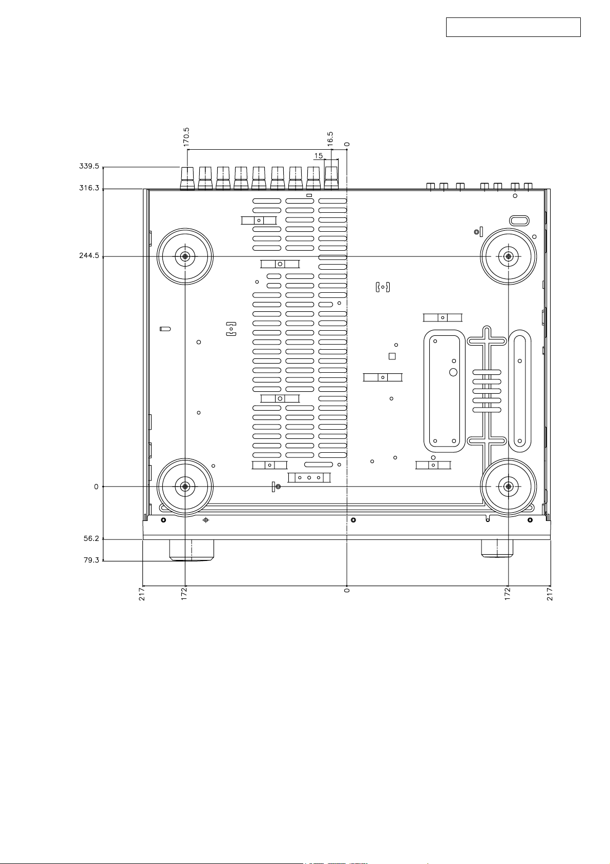
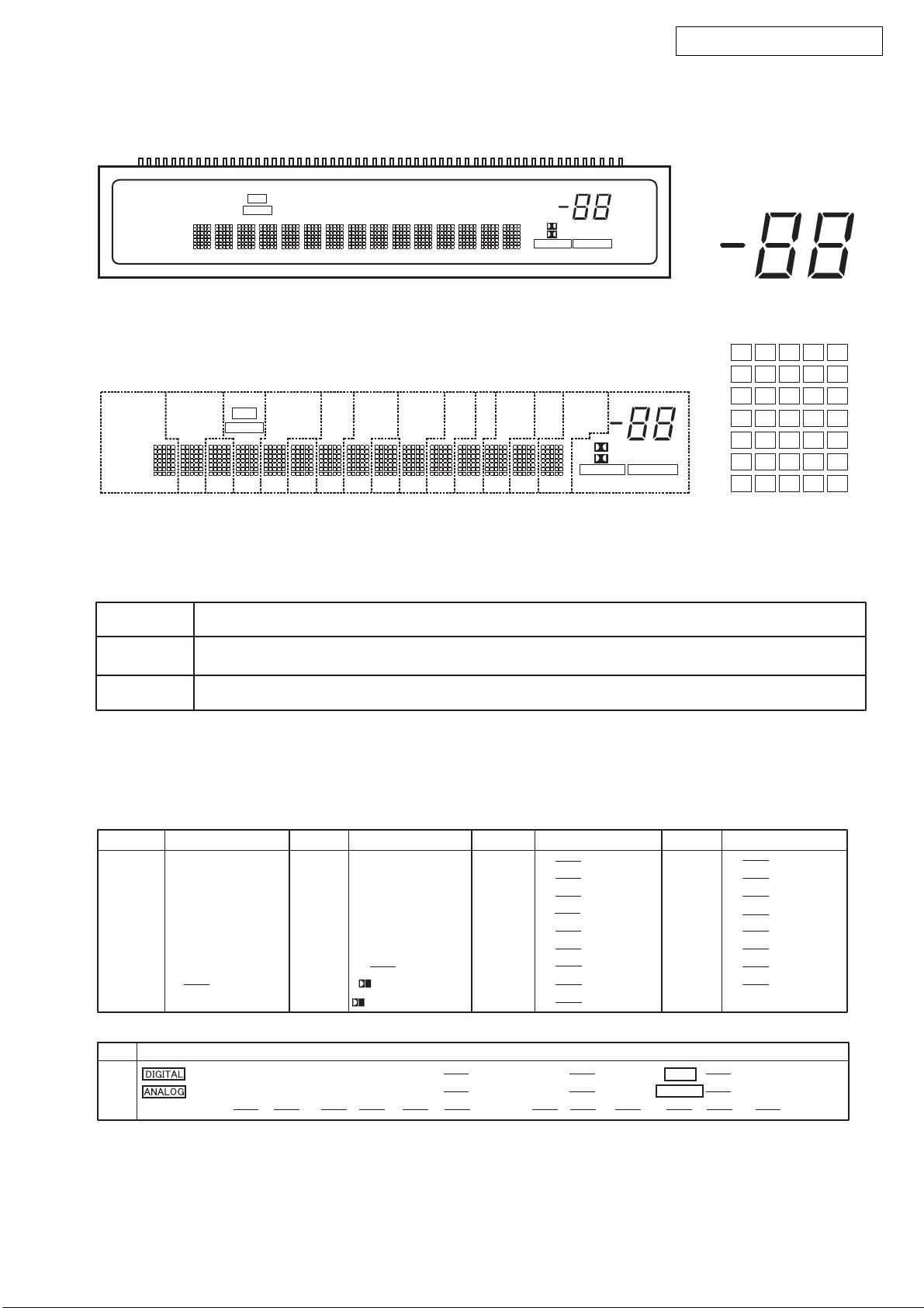
DIMENSION
AVR-1905/785 AVC-1590
3

AVR-1905/785 AVC-1590
CAUTION IN SERVICING
Initializing AV SURROUND RECEIVER
AV SURROUND RECEIVER initialization should be performed
when the µcom, peripheral parts of µcom, and Digital P.W.B. are
replaced.
1. Switch off the unit.
2. Hold the following SPEAKERS-A button and SPEAKERS-B
button, and switch on the unit.
3. Check that the entire display is flashing with an interval of
about 1 second, and release your fingers from the 2 buttons
and the microprocessor will be initialized.
Note:・If step 3 does not work, start over from step 1.
・ All user settings will be lost and this factory setting will
be recovered when this initialization mode.
So make sure to memorize your setting for restoring
after the initialization.
サービス時の注意事項
AVサラウンドアンプの初期化について
マイコンやマイコン周辺部品、Digital基板等を交換した場合
は、AVサラウンドアンプの初期化を行って下さい。
1.オン/オフボタンをOFFにします。
2.SPEAKERS-AボタンとSPEAKERS-Bボタンを同時に押しな
がら、オン/オフボタンを押してONにします。
3.ディスプレイ表示が約1秒間隔で点滅するのを確認後、2
つのボタンから指を離します。
*マイコンが初期化されます。
注意:・上記3の状態にならない場合は、もう一度操作1か
らやり直してください。
・初期化を行うとお客様が設定した内容が工場出荷状
態に戻りますので、あらかじめ設定内容を控えてお
き初期化後再設定してください。
4
AVR-1905/785 AVC-1590
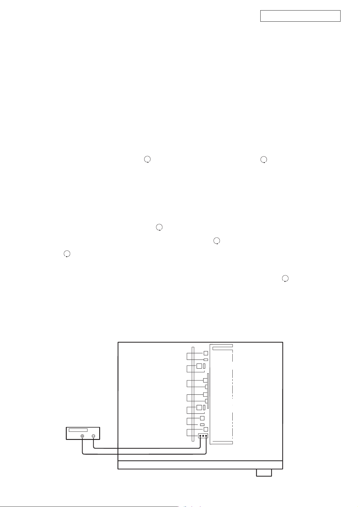
ADJUSTMENT
Audio Section
Idling Current
Required measurement equipment: DC Voltmeter
1. Preparation
(1) Avoid direct blow from an air conditioner or an electric
fan, and adjust the unit at normal room temperature 15 °C
~ 30 °C (59 °F ~ 86 °F).
(2) Presetting
• POWER (Power source switch) OFF
• SPEAKER (Speaker terminal) No load
(Do not connect speaker, dummy resistor, etc.)
2. Adjustment
(1) Remove top cover and set VR101, VR102, VR103,
VR104, VR105, on Amp. Unit, VR106 on SURR.-BACK
ch Amp. Unit at fully counterclockwise ( ) position.
(2) Connect DC Voltmeter to test points (FRONT-Lch:
TP104, FRONT-Rch: TP105, CENTER ch: TP103, SURROUND-Lch: TP101, SURROUND-Rch: TP102, SURROUND-BACK Lch: TP106,SURROUND-BACK Rch:
TP107).
(3) Connect power cord to AC Line, and turn power switch
"ON".
(4) Presetting.
MASTER VOLUME : "---" counterclockwise ( min.)
MODE : 6CH STEREO
FUNCTION : CD
(5) Within 2 minutes after the power on, turn VR101 clock-
wise ( ) to adjust the TEST POINT voltage to 1.5 mV
± 0.5 mV DC.
(6) After 10 minutes from the preset above, turn VR101 to
set the voltage to 2.5 mV ± 0.5 mV DC.
(7) Adjust the Variable Resistors of other channels in the
same way.
調整
オーディオセクション
アイドリング電流の調整
調整に必要な測定器: DCVoltmeter
1.準備
(1)セットをクーラ、扇風機のそばなど風通しの良い場所
を避け、通常の使用状態に置きます。セットの周囲温
度は15〜30℃、湿度は常湿とします。
(2)プリセット
・電源スイッチOFF
・スピーカ端子無負荷
(スピーカ・ダミー抵抗器などを接続しない。)
2.調整
(1)上カバーをはずし、パワーアンプ基板のVR101,VR102,
VR103,VR104,VR105及びSURR.-BACKアンプ基板の
VR106を反時計方向()に回し切った状態にセット
します。
(2)テストポイント(FRONT-Lch:TP104,FRONT-Rch:
TP105,CENTERch:TP103,SURROUND-Lch:TP101,
SURROUND-Rch:TP102,SURROUND-BACKLch:
TP106,SURROUND-BACKRch:TP107)にDCVoltmeter
を接続します。
(3)電源コードをAC100V(95〜105Vの範囲でも可)に接
続し、電源スイッチを"ON"にします。
(4)ON後、次のようにセットします。
・MASTERVOLUME(音量調節つまみ)→反時計方向
()に回す、最小の状態にする。
・SPEAKER(スピーカ端子)→無負荷(スピーカ、
ダミー抵抗器などを接続しない。)
MODE:6CHSTEREO
FUNCTION:CD
(5)2分以内にVR101を時計方向()に回しテストポイ
ントの電圧を次のように調整します。
1.5mV±0.5mVDC
(6)予備調整から10分後VR101を回し、次のように電圧を
設定します。
2.5mV±0.5mVDC
(7)同じ方法で各チャネルの可変抵抗を調整します。
DC Voltmeter
F Lch
S Lch
S Back Rch
S Back Lch
C ch
S Rch
F Rch
VR104
TP104
VR101,TP101
TP107
VR107SBR
TP106
VR107SBL
VR103,TP103
VR102
TP102
VR105
TP105
5

AVR-1905/785 AVC-1590
Video Section
Component Video Level Adjustment
Required measurement equipment etc.: Oscilloscope, DVD
VIDEO PLAYER (ex: DVD-1500)
Test disc: DVD T-S01
1. Preparation
(1) Avoid direct blow from an air conditioner or an electric
fan, and adjust the unit at normal room temperature 15 °C
~ 30 °C (59 °F ~ 86 °F).
(2) Playback the color-bar 75% of the Test Disc (Title 12) us-
ing the DVD Video Player, and check that Y and C levels
of the S terminal output are within the specified output
levels.
If they are out of the specified levels, adjust with the variable resister inside of the unit.
(3) Presetting
• POWER (Power source switch) OFF
• SPEAKER (Speaker terminal) No load
(Do not connect speaker, dummy resistor, etc.)
• DVD (Video terminal) No input
2. Adjustment
(1) Remove top cover and set VR601, VR602, VR603, on C-
S VIDEO2 Unit at fully counterclockwise ( ).
(2) Connect a pin-plug terminated with 75-ohms to Y (Cb, Cr)
of the Component Video Monitor Output, and hook up the
Oscilloscope’s probe to both ends of the pin-plug.
(3) Connect S terminal output of the DVD Player with the
DVD input terminal of the Receiver.
(4) Connect power cord to AC Line, and turn power switch
"ON".
(5) Presetting.
• FUNCTION: DVD
• Playback the color-bar 75% of the Test Disc (Title 12)
(6) Turn VR601 clockwise ( ) to adjust the COMPONENT
Video Y voltage (except H. Sync) to 714 ± 50 mVp-p. (Refer to Fig. 1)
(7) Adjust the Variable Resistors of Cr: VR602 and Cb:
VR603 in the same way. (Refer to Fig. 2, 3)
Cb,Cr: 486 ± 50 mVp-p. (U.S.A. & Canada model)
525 ± 50 mVp-p. (Others)
ビデオセクション
コンポーネントビデオレベルの調整
調整に必要な測定器:Oscilloscope,DVDVIDEOPLAYER
(例:DVD-1500)
テストディスク:DVDT-S01
1.準備
(1)セットをクーラ、扇風機のそばなど風通しの良い場所
を避け、通常の使用状態に置きます。セットの周囲温
度は15〜30℃、湿度は常湿とします。
(2)DVDVIDEOPLAYERでテストディスクのカラーバー
75%(Title12)を再生し、S端子出力Y、Cレベルが正規
の出力レベルであることを確認する。正規の出力レベ
ルでない場合は、セット内部の可変抵抗器で調整して
ください。
(3)プリセット
・電源スイッチOFF
・スピーカ端子無負荷
(スピーカ・ダミー抵抗器などを接続しない。)
・DVD入力端子無入力
2.調整
(1)上カバーをはずし、C-SVIDEO2ユニットのVR601,
VR602,VR603を反時計方向()に回し切った状態に
セットします。
(2)コンポーネントビデオモニターアウトのY(Cb,Cr)に
75Ωで終端したピンプラグを接続し、その両端を
Oscilloscopeのプローブでつまみます。
(3)DVDVIDEOPLAYERのS端子出力を本機のDVD入力端
子に接続します。
(4)電源コードを電源コンセントに接続し、電源スイッチ
を"ON"にします。
(5)ON後、次のようにセットします。
・本機のFUNCTIONをDVDにする。
・テストディスクのカラーバー75%(Title12)を再生す
る。
(6)VR601を時計方向()に回しコンポーネントビデオ
Y(H.Syncを除く)の電圧を調整します。(Fig.1参照)
714mV±50mVp-p
(7)同じ方法でCr:VR602、Cb:VR603の可変抵抗器を調整
します。(fig.2、3参照)
Cb,Cr:525±50mVp-p
6

Oscilloscope
VR903
Cb
Cr
AVR-1905/785 AVC-1590
MONITOR OUT
(Y,Cb,Cr)
Y
VR902VR901
Video Section
7
AVR-1905/785 AVC-1590
Volts
IRE:FLT
100.0
0.5
0.0
0.5
-20.0 -10.0 0.0
Volts
0.5
IRE:FLT
50.0
Y-Signal
714±50mV
p-p
10.0
20.0 30.0
Fig.1 Component Video Y signal
40.0 50.0 60.0
486±50mV (U.S.A. & Canada model)
p-p
0.0
-0.5
Volts
0.5
0.0
0.0
-50.0
0.0
IRE:FLT
50.0
0.0
-50.0
20.0
Fig.2 Cb signal
40.0
60.0
486±50mV (U.S.A. & Canada model)
80.0
p-p
-0.5
0.0
20.0
Fig.3 Cr signal
8
40.0
60.0
80.0
BLOCK DIAGRAM
AVR-1905/785 AVC-1590
DIGITAL OUT
OPTICAL
DIGITAL IN
COAXIAL
OPTICAL 1
OPTICAL 2
ANALOG IN
DVD/VDP
TV/DBS
CDR/TAPE
ANALOG OUT
CDR/TAPE
FRONT IN
OPTICAL 3
V.AUX L/R
V.AUX VIDEO
MULTI OUT
E3 ONLY
ANALOG IN
6CH_INPUT
TUNER PART
AUX
VCR
VCR
TUNER
FM ANT
AM ANT
CD
SW
SR
DSP
ROM
TC9273-004
REC_SWITCHIG
12.288MHZ
INPUT
Selector
X-TAL
DIR
LC89057W-VF4
DeModulate
&
Lock Detect
XMCK
FROM
MICOM
BD3811K1
RDATA(21)
SLRCK(23)
SBCK(22)
DATA
Selector
ADIN
(24)
ASDATA
AUDIO
DIRERR
CCLK
CLATCH
CIN
COUT
BSE
SELCLK
ERRMUTE SERIAL DATA
DACRST I/O PORT
128k X 8
RAM
128k X 8
256fs
64fs
fs
ALRCK
MCLK
ABCLK
DBCLK
DLRCLK
DSDATA2
DSDATA1
DSDATA3
DSDATA4
DAI_P20(94)
DAI_P11(78)
DAI_P12(79)
CLKIN
CONTROL PORT
VOLUME
VOLUME
VOLUME
DIGITAL AUDIO DECODER
ADSP-21266
DAI_P10(77)
DAI_P9(71)
X-TAL
25MHZ
74LVX157MCT SELECTOR
CLOCK
DIGITAL
DAC
FILTER
DIGITAL
DAC
FILTER
DIGITAL
DAC
FILTER
CLKIN(142)
DAI_P13(80)
DAI_P14(81)
DACFRSRDATA
DACSBLCDATA
DACSWSBDATA
+
+
+
DAI_P16(82)
DAI_P15(81)
DACFLSLDATA
MUTE
SDOUT
-
-
+
LR
+
INPUT SELECTOR & VOLUME
L
+
R
+
+
HPF
DIGITAL
ADC
FILTER
DIGITAL
ADC
FILTER
AUDIO CODEC
AD1837
VOLUME
VOLUME
VOLUME
VOLUME
VOLUME
DIGITAL
FILTER
DIGITAL
FILTER
DIGITAL
FILTER
DIGITAL
FILTER
DIGITAL
FILTER
DAC
DAC
DAC
DAC
DAC
+
+
+
+
+
VIDEO INPUT
DVD/VDP
TV/DBS
VCR
<AVC1590 ONLY>
FL
FR
C
SL
FM
FRONTEND
IF FILTER
IF AMP
IF FILTER
FM&AM
IF IC
MPX IC
AM TUNING
PLL CIRCUITLOOP FILTER
L.P.F
MUTING
<AVR1905 ONLY>
VCR OUT
MONITOR OUT
DVD/VDP
TV/DBS
VCR OUT
MONITOR OUT
RMC IN
RMC OUT
DVD/VDP
TV/DBS
FROM u-COM
VIDEO SWITCH
BA7626
S-VIDEO INPUT
VCR
VIDEO SWITCH
CXA1511M
COMPONENT,D-VIDEO VIDEO INPUT
VCR
(C,Y)BA7626*2
MONITOR OUT
AVC1590 / AVR1905 BLOCK DIAGRAM
RESET(121)
SPICS(122)
SPICLK(125)
MISO(126)
MOSI(127)
FLAG3(98)
FLAG2(97)
FLAG1(16)
FLAG0(15)
SW F
MIXING
-
-
-
74HC4053
Y/C MIX
NJM2274
DATA IN (REMOCON)
+5.6V(CPU)
Q0,Q1
VIDEO SWITCH
BA7625*1,BA7626*2
( Y, B-Y, R-Y )
OSD
Y/C
TC90A69F
SEPARATE
FROM
MICOM
-
-
-
74HC4053
SEPARATE
Y/Cb/Cr
TA1270
Y
Cb
Cr
TUNER PLL
Y
Cb
Cr
DATA
+6V
74HC4053
RESONATOR
12MHz
CXP740096
DTS-ES/DD-EX/PL IIX
ANA_IN
DSP_FL
EX_FL
ANA_IN
DSP_FR
EX_FR
CENTER
EX_SL
SL
EX_SR
SR
EX_C
SW
EX_SW
SBL
MULTI_L
SBR
MULTI_R
MUTE
MICOM
PART DATA
BD3811K1
A/D POWER
KEY_MATRIX
VIDEO
VIDEO
VIDEO
MICOM, FLT DRV
RMC_IN/OUT
DSP
DIR
ENCODER
CODEC
RELAY
+5V
OP AMP
INPUT/VOL
TUNER
INPUT/VOL
OP AMP
MAIN +B
MAIN -B
FLT DRIVER
2CH-VOLUME IC
BD3812F
+1.2V
+3.3V
7805
7812
DATA
7806
7906
7809
7805
7805
7815
7915
FL DRIVER
LC75721NE
-VKK
FILAMENT AC
16-ST-66GNK
FL DISPLAY
L
GND
H/P OUT
+
+
+
+
+
+
+
-
+
-
+
-
+
-
+
-
R
FL
SPK A
FR
FL
SPK B
FR
CENTER
SPEAKER OUT
+
+
+
+
+
MUTE
+
+
+
+
+
SURR L
-
+
SURR R
-
+
SBL
-
+
SBR
-
FR
PRE OUT
FL
SW
C
SR
SL
SBR
SBL
AC CORD
AC OUTLET
9
LEVEL DIAGRAMS (1/2)
AVR-1905/785 AVC-1590
DIGITAL
6CH IN
6CH IN
CD IN
6CH IN
40dB
30dB
20dB
10dB
0dB
(200mV)
-10dB
-20dB
FRONT
6CH IN
CD IN
INPUT
BUFFER
AMP
+
A/D IN
REV AMP
---
-12dB
A/D IN
A/D IN
REV AMP
REV AMP
0dBFS
-10dBFS
-20dBFS
-30dBFS
A/D
DIR
A/D
DSP
D/A OUT
100mV REF
HPF
+
D/A
0dBFS
-10dBFS
-20dBFS
-30dBFS
D/A
D/A OUT
LPF
+--
MUTE
6dB
REV AMP
SW SUM
REV AMP
--
SUM S/W
-18dB
ELECTRIC
VOLUME
BD3811K1
BD3811K1
VOL 00
TONE
PRE AMP POWER AMP
+
MUTE
16dB
25.5dB
-35.5dB
ATT
SPK OUT
FRONT
H/P OUT
SPK OUT
FRONT
2.83V
(1W/8ohm)
H/P OUT
47mV
(0.27mW)
40dB
30dB
20dB
10dB
0dB6CH IN
(200mV)
-10dB
-20dB
CENTER
SURROUND
SURROUND-BACK
DSP OUT
DSP OUT
D/A OUT
100mV REF
D/A
D/A
0dBFS
-10dBFS
-20dBFS
-23dBFS
-30dBFS
D/A
SPK OUT
+
MUTE
BD3812F
+
MUTE
CENTER
6dB
SL/SR/SBL/SBR
-15dB
-18dB
VOL 00
+
MUTE
+
MUTE
25.5dB
16dB
CENTER
SURROUND
SPK OUT
SURROUND
BACK
SPK OUT
2.83V
(1W/8ohm)
10
LEVEL DIAGRAMS (2/2)
AVR-1905/785 AVC-1590
SUB_WOOFER
6CH INPUT
30dB
20dB
10dB
6CH IN
(200mV)
(112mV)
OdB
-8dB
-10dB
-20dB
-30dB
DSP OUT
0dBFS
-10dBFS
-20dBFS
Config2 -28dBFS
-30dBFS
Config1 -38dBFS
D/A
D/A
LFE
LFE
D/A OUT
LPF
+
Front D/A Out
100mV ref
6dB
6dB
MUTE
REV AMP
--
SW SUM
REV AMP
-- +
TO FRONT CH
10.5dB
10dB
ELECTRIC
VOLUME
BD3811K1
-18dB
VOL 00
PRE AMP
28dB
MUTE
SUB WOOFER
PRE OUT
SUB WOOFER
PRE OUT
500mV
11
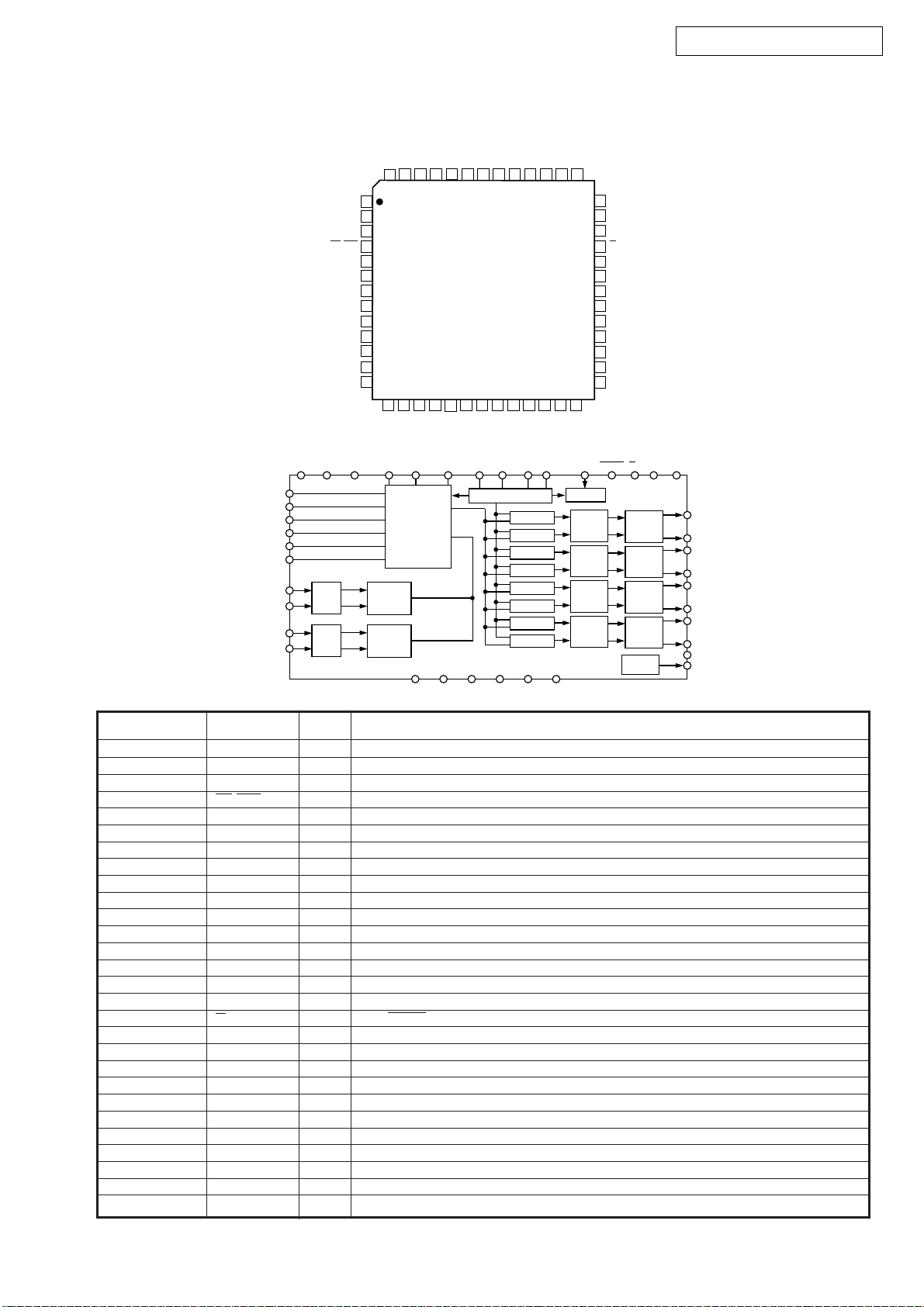
SEMICONDUCTORS
Only major semiconductors are shown, general semiconductors etc. are omitted to list.
主な半導体を記載しています。汎用の半導体は記載を省略しています。
1. IC’s
CXP740010-192Q (IC201)
DDVSS
PK1/TX
PK2/TEX
PI1/RMC
PI2/NMI
PI3/TO0/ADJ
PI4/INT1/CS1
PI5/SCK1
80
79
78
77
76
75
74
73
72
71
70
69
68
67
66
65
64
63
62
61
60
59
58
57
56
55
54
53
52
51
50
PC5
PC4
PC3
PC2
PC1
PC0
PB7/SI2
PB6/SO2
PB5/SCK2
PB4/TO2
PB3
PB2
PB1
PB0
PJ7
PJ6
PJ5
PJ4
PJ3
PJ2
PJ1
PJ0
PD7
PD6
PD5
PD4
PD3
PD2
PD1
PD0
PC6
PC7
PA0
PA1
PA2
PA3
PA4
PA5
PA6
PA7NCV
99989796959493929190898887868584838281
100
1
2
3
4
5
6
7
8
9
10
11
12
13
14
15
16
17
18
19
20
21
22
23
24
25
26
27
28
29
30
31323334353637383940414243444546474849
TOP VIEW
PI6/SO1
PI7/SI1
PE0/INT0
PE1/INT2
PE2/PWM0
PE3/PWM1
PE4
PE5
PE6
PE7
PG0/TxD
PG1/RxD
PG2/EC0
PG3/EC1
PG4/EC2
PG5/INT3
PG6/INT4
PG7/CINT
AN0
AN1
AN2
AN3
PF0/AN4
PF1/AN5
PF2/AN6
PF3/AN7
AV
DD
AV
REF
AV
SS
PF4/AN8
AVR-1905/785 AVC-1590
SS
PH7
PH6
PH5
PH4
PH3
PH2
PH1
PH0
PK7/TO1
RST
V
XTAL
EXTAL
PK6/CS0
CXP740010-192Q Terminal Function
Pin
No.
1 BD3811K1/3812F_MUTE O BD3811K/BD3812F MUTE CONTROL
2 BD3811K1/3812F_CLK O BD3811K/BD3812F CLOCK
3 BD3811K1/3812F_DATA O BD3811K/BD3812F DATA
4 MULTI MUTE O MULTI MUTE
5 VCR O VCR MUTE
6 ERR_MUTE O ERR MUTE
7 SEL_CLK O SEL_CLK
8 BSE O AC3MUTE MUTE for BITSTREAM
9 89057_EMPHA I LC89057 CONTROL
10 SW_SUM O SW SUMMING CONTROL
11 SHARC_SDIN I SHARC EX(DSP) DATA INPUT
12 89057_SDIN I LC89057 CONTROL
13 EPROM_RESET O EPROM RESET
14 89057_RESET O LC89057 RESET
15 SHARC_CS O SHARC EX(DSP) CS
16 SHARC_SDOUT O SHARC EX(DSP) DATA OUTPUT
17 89057_CE O LC89057 CONTROL
18 89057/1837_SDOUT O CONTROL DATA
19 89057/1837_SCLK O CONTROL CLOCK
20 1837_RESET O CODEC RESET
21 REELAY_SURR_B O SURROUND BACK RELAY
22 SW_MUTE O SW MUTE
Pin Name I/O Function
PK5/SI0
PK4/SO0
PK3/SCK0
PF5/AN9
PF7/AN11
PF6/AN10
12

AVR-1905/785 AVC-1590
Pin
No.
23 RELAY_FRONT_B O FRONT B RELAY
24 RELAY_FRONT_A O FRONT A RELAY
25 RELAY_SURR O SURROUND RELAY
26 RELAY_CNT O CENTER RELAY
27 RELAY_H/P O RELAY H/P
28 FUNC_UP O ENCODER INPUT (FUNCTION)
29 H/P_DETECT I DETECT H/P
30 FUNC_DOWN O ENCODER INPUT (FUNCTION)
31 SURR_SB_MUTE O SURROUND BACK MUTE
32 CNT_MUTE O CENTER MUTE
33 RLY MULTI O -
34 SURR_MUTE O SURROUND MUTE
35 TC9273 STB O TC9273 STB
36 TC9273 CLK O TC9273 CLK
37 TC9273 DATA O TC9273 DATA
38 FL_DRV_RST O LC75721 RESET
39 RELAY_POWER O POWER RELAY
40 RESET I RESET
41 GND GND
42 XTAL CRISTAL OSIRATER CONNECTION
43 EXTAL CRISTAL OSIRATER CONNECTION
44 FL_DRV_CE O LC75721 CE
45 FL_DRV_DATA O LC75721 DATA
46 FL_DRV/2090_CLK O LC75721/BU2090 CLOCK
47 2090_DATA O BU2090 DATA
48 VOL_DOWN I ENCODER INPUT (VOLUME)
49 VOL_UP I ENCODER INPUT (VOLUME)
50 SEL_DOWN I ENCODER INPUT (SELECTOR)
51 SEL_UP I ENCODER INPUT (SELECTOR)
52 AV
53 V
54 AVDD AVD D
55 S-VIDEO_DET I S Signal Detect input
56 COPM_DET I Compornent Signal input
57 STEP_OPT I AREA SELECT
58 SET_OPT I MODEL SELECT
59 GND GND
60 KEY_IN3 I KEY INPUT
61 KEY_IN2 I KEY INPUT
62 KEY_IN1 I KEY INPUT
63 C-VIDEO_DET I Composit Signal Detect input
64 PROTECT I PROTECTION
65 89057_INT LC89057 INT
66 SHARC_SCLK O SHARC EX(DSP) SCLK
67 1837_CE O CODEC CE
68 SHARC_RESET O SHARC EX(DSP) RESET
69 FRONT_MUTE O FRONT MUTE
70 PWR_DOWN I POWER DOWN DETECT
71 NC - -
72 NC - -
73 LC74781 SOUT O LC74781 SOUT
74 NC - -
75 TA1270_TC90A69 DATA O TA1270/TC90A69 DATA
76 TA1270_TC90A69 CLK O TA1270/TC90A69 SCLK
77 RDS_DATA I RDS(TDA7330) DATA
Pin Name I/O Function
SS AVSS
REF VREF
13
AVR-1905/785 AVC-1590
Pin
No.
78 RDS_CLK I RDS(TDA7330) CLOCK
79 FLAG3 I Special flag for ROM update
80 FLAG2 I DSP operation check flag
81 FLAG1 I NON USE
82 FLAG0 I EPROM chip select control for DSP
83 LC74781 SCLK O LC74781 SCLK
84 LC74781 CS O LC74781 CS
85 REMOCON REMOTE CONTROL SIGNAL INPUT
86 S-MONI DET I VIDEO S-SIGNAL MONITOR DETECT
87 GND GND
88 V
89 V
90 NC - -
91 2090 DATA2 O BU2090 DATA2(VIDEO)
92 PLL_DATA O PLL CONTROL (LC72131)
93 PLL_CLK O PLL CONTROL (LC72131)
94 PLL_DT_IN I PLL CONTROL (LC72131)
95 TU_MUTE O TUNER MUTE
96 ST I STEREO DETECT
97 TUNED I TUNE DETECT
98 PLL_CE O PLL CONTROL (LC72131)
99 2090_CLK(VIDEO) O BU2090 CLK (VIDEO)
100 2090_DATA(VIDEO) O BU2090 DATA (VIDEO)
Pin Name I/O Function
SS VSS
DD(BACK UP) VDD FOR BACK UP
14
ADSP-21266SKSTZ-1B (IC804)
AVR-1905/785 AVC-1590
144
1
36
37
PIN 1 INDICATOR
TOP VIEW
109
108
73
72
ADSP-21266SKSTZ-1B Terminal Function
LQFP
Pin Name
V
DDINT
Pin # Pin Name
1V
DDINT
CLKCFG0 2 GND 38 GND 74 V
CLKCFG1 3 RD 39 V
BOOTCFG0 4 ALE 40 GND 76 V
LQFP
Pin # Pin Name
37 V
DDEXT
DDINT
LQFP
Pin # Pin Name
73 GND 109
DDINT
75 GND 111
DDINT
BOOTCFG1 5 AD15 41 DAI_P10 (SD2B) 77 GND 113
GND 6 AD14 42 DAI_P11 (SD3A) 78 V
V
DDEXT
7 AD13 43 DAI_P12 (SD3B) 79 GND 115
GND 8 GND 44 DAI_P13 (SCLK23) 80 V
V
DDINT
9V
DDEXT
45 DAI_P14 (SFS23) 81 GND 117
GND 10 AD12 46 DAI_P15 (SD4A) 82 V
V
DDINT
11 V
DDINT
47 V
DDINT
83 GND 119
GND 12 GND 48 GND 84 V
V
DDINT
13 AD11 49 GND 85 RESET 121
DDINT
DDEXT
DDINT
DDINT
GND 14 AD10 50 DAI_P16 (SD4B) 86 SPIDS 122
FLAG0 15 AD9 51 DAI_P17 (SD5A) 87 GND 123
FLAG1 16 AD8 52 DAI_P18 (SD5B) 88 V
DDINT
AD7 17 DAI_P1 (SD0A) 53 DAI_P19 (SCLK45) 89 SPICLK 125
GND 18 V
V
DDINT
19 GND 55 GND 91 MOSI 127
DDINT
54 V
DDINT
90 MISO 126
GND 20 DAI_P2 (SD0B) 56 GND 92 GND 128
V
DDEXT
GND 22 GND 58 DAI_P20 (SFS45) 94 V
V
DDINT
AD6 24 V
21 DAI_P3 (SCLK0) 57 V
23 V
DDEXT
DDINT
59 GND 95 A
60 V
DDEXT
DDINT
93 V
96 A
DDINT
DDEXT
VDD
VSS
AD5 25 GND 61 FLAG2 97 GND 133
AD4 26 DAI_P4 (SFS0) 62 FLAG3 98 CLKOUT 134
V
DDINT
27 DAI_P5 (SD1A) 63 V
DDINT
99 EMU 135
GND 28 DAI_P6 (SD1B) 64 GND 100 TDO 136
AD3 29 DAI_P7 (SCLK1) 65 V
AD2 30 V
V
DDEXT
31 GND 67 V
GND 32 V
DDINT
DDINT
66 GND 102 TRST 138
68 GND 104 TMS 140
AD1 33 GND 69 V
DDINT
DDINT
DDINT
101 TDI 137
103 TCK 139
105 GND 141
AD0 34 DAI_P8 (SFS1) 70 GND 106 CLKIN 142
WR 35 DAI_P9 (SD2A) 71 V
V
DDINT
36 V
DDINT
72 V
DDINT
DDINT
107 XTAL 143
108 V
DDEXT
LQFP
Pin #
110
112
114
116
118
120
124
129
130
131
132
144
15

LC89057W (IC807)
AVR-1905/785 AVC-1590
RXOUT
RX0
RX1
RX2
RX3
RX4
RX5/VI
RX6/UI
LPF
TMCK/PIO0
TBCK/PIO1
TLRCK/PIO2
TDATA/PIO3
TXO/PIOEN
1
2
3
4
5
8
9
10
13
44
45
46
47
48
EMPHA/UO33AUDIO/VO35INT40CL39CE38DI
32
Microcontroller
Clock
27
Input
Selector
Modulation
or
Parallel Port
29
XIN
C bit, U bit
Demodulation
&
Lock Detect
PLL
28
XOUT
Selector
XMCK34CKST
I/F
Data
Selector
I/N
XMODE
41
37
36
21
24
16
17
20
22
23
DO
RERR
RD ATA
SDIN
RMCK
RBCK
RLRCK
SBCK
SLRCK
36 RERR1RXOUT
35 INT2RX0
34 CKST3RX1
TOP VIEW
33 AUDIO/VO4RX2
32 EMPHA/UO5RX3
31 DGND6DGND
30 DVDD7DVDD
29 XIN8RX4
28 XOUT9RX5/VI
27 XMCK10RX6/UI
26 DVDD11DVDD
25 DGND12DGND
24 SDIN37DO
23 SLRCK38DI
22 SBCK39CE
21 RDATA40CL
20 RLRCK41XMODE
19 DVDD42DGND
18 DGND43DVDD
17 RBCK44TMCK/PIO0
16 RMCK45TBCK/PIO1
15 AGND46TLRCK/PIO2
14 AVDD47TDATA/PIO3
13 LPF48TXO/PIOEN
LC89057W Terminal Function
Pin
No.
1 RXOUT O Input bi-phase select data output terminal
2 RX0 I TTL compatible digital data input terminal
3 RX1 I Coaxial compatible amp built-in digital data input terminal
4 RX2 I TTL compatible digital data input terminal
5 RX3 I TTL compatible digital data input terminal
6 DGND — Digital GND
7 DVDD — Digital power
8 RX4 I TTL compatible digital data input terminal
9 RX5/VI I TTL compatible digital data/Validity flag input terminal for modulation
10 RX6/UI I TTL compatible digital data/User data input terminal for modulation
11 DVDD — Digital power for PLL
12 DGND — Digital GND for PLL
13 LPF O PLL loop filter connecting terminal
14 AVDD — Analog power for PLL
15 AGND — Analog GND for PLL
16 RMCK O RMCK clock output terminal (256fs, 512fs, XIN, VCO)
17 RBCK O/I RBCK clock in/output terminal (64fs)
18 DGND — Digital GND
19 DVDD — Digital power
20 RLRCK O/I RLRCK clock in/output terminal (fs)
21 RDATA O Serial audio data output terminal
22 SBCK O SBCK clock output terminal (32fs, 64fs, 128fs)
23 SLRCK O SLRCK clock output terminal (fs/2, fs, 2fs)
24 SDIN I Serial audio data input terminal
25 DGND — Digital GND
26 DVDD — Digital power
27 XMCK O Osc. amp output terminal
Pin Name
I/O
Function
16
AVR-1905/785 AVC-1590
Pin
No.
Pin Name I/O
Function
28 XOUT O X’tal osc. connecting output terminal
29 XIN I X’tal osc. connection, external clock input terminal (24.576MHz or 12.288MHz)
30 DVDD — Digital power
31 DGND — Digital GND
32 EMPHA/UO I/O Emphasis information/U-data output/Chip address setting terminal
33 AUDIO/VO I/O Non-PCM detect/V-flag output/ Chip address setting terminal
34 CKST I/O Clock switch transition period output/Demodulation master or slave function switching terminal
35 INT I/O Interrupt output for µcom (Interrupt factor selectable)/Modulation or general I/O switching terminal
36 RERR O PLL lock error, data error flag output
37 DO O µcom I/F, read out data output terminal (3-state)
38 DI I µcom I/F, write data input terminal
39 CE I µcom I/F, chip enable input terminal
40 CL I µcom I/F, clock input terminal
41 XMODE I System reset input terminal
42 DGND — Digital GND
43 DVDD — Digital power
44 TMCK/PIO0 I/O 256fs system clock input for modulation/General I/O in/output terminal
45 TBCK/PIO1 I/O 64fs bit clock input for modulation/General I/O in/output terminal
46 TLRCK/PIO2 I/O fs clock input for modulation/General I/O in/output terminal
47 TDATA/PIO3 I/O Serial audio data input for modulation/General I/O in/output terminal
48 TXO/PIOEN O/I Modulation data output/ General I/O enable input terminal
* For latch-up countermeasure, perform each power supply ON/OFF in the same timing.
BD3811K1 (IC701)
IN31
IN32
IN41
IN42
IN51
IN52
IN61
IN62
IN71
IN72
IN81
IN82
INDVDSR
INDVDSL
INDVDC
INDVDSW
OUT2(+)
OUT2(-)
OUT1(+)
OUT1(-)
IN1DSP
IN1MIX
IN2DSP
IN2MIX
IN22
IN21
IN12
IN11
ROUT32
ROUT31
ROUT22
ROUT21
ROUT12
ROUT11
AGND10
GOUT2
OUTC
VIN2
LOGIC
OUTSL
80 79 78 77 76 75 74 73 72 71 70 69 68 67 66 65
1
2
3
4
5
6
7
8
9
10
11
12
13
14
15
16
17
18
19
20
21
22
23
24
25 26
5.1ch Mode SW2 DSP
27 28 29 30 31 32 33 34 35 36 37 38 39 40
INDSPC
INDSPSL
INDSPSR
5.1ch Mode SW2 DVD
AGND1
INDSPSW
GOUTSW
VINSW
AGND2
5.1ch Mode SW1
VINC
GOUTC
OUTSW
AGND9
TREBLE
BASS
BASS
BOOST
OUTSR
GOUT1
VINSL
VIN1
GOUTSL
64
63
62
61
60
59
58
57
56
55
54
53
52
51
50
49
48
47
46
45
44
43
42
41
TNF2
TNF1
BNF11
BNF21
BNF12
BNF22
BBNF2
OUT2
BBNF1
OUT1
AGND8
AGND7
VCC
AGND6
VEE
AGND5
MUTE
CL
DA
DGND
AGND4
GOUTSR
VINSR
AGND3
17
AD1837 (IC808)
AVR-1905/785 AVC-1590
DSDATA3
DSDATA2
AGND
DGND
DSDATA1
39
38
37
36
35
34
33
32
31
30
29
28
27
NC
OUTL3
MCLKASDATAABCLKALRCLKODVDDDVDD DVDD
PD/RST M/S AVDD AVDD
CLOCK
DIGITAL
FILTER
DIGITAL
FILTER
DIGITAL
FILTER
DIGITAL
FILTER
DescriptionPin No.
DVDD
DBCLK
DLRCLK
M/S
AGND
OUTR4
NC
OUTL4
NC
AGND
AVDD
OUTR3
NC
VREF
Σ-∆
DAC
Σ-
DAC
Σ-
DAC
Σ-
DAC
OUTL1
OUTR1
∆
∆
∆
OUTL2
OUTR2
OUTL3
OUTR3
OUTL4
OUTR4
FILTD
FILTR
DLRCLK
DBCLK
DSDATA1
DSDATA2
DSDATA3
DSDATA4
ADCLP
ADCLN
ADCRP
ADCRN
AD1837 Terminal Function
Pin Name
CLATCH
PD/RST
Σ-∆
ADC
∆
Σ-
ADC
AD1837
Input/
Output
DVDD
CIN
AGND
NC
OUTL1
NC
OUTR1
AGND
AVDD
NC
OUTL2
DGND
CCLK
COUT
ASDATA
ODVDD
MCLK
ALRCLK
ABCLK
50 494847 46 45 44 43 42 41 40
51
52
1
2
3
4
5
6
7
8
9
10
11
12
13
14 15 16 17 18 19 20 21 22 23 24 25 26
NC
OUTR2
SERIAL DATA
I/O PORT
DIGITAL
FILTER
DIGITAL
FILTER
TOP VIEW
FILTD
FILTR
AGND
DGND AGND AGND AGND AGNDDGND
AVDD
DSDATA4
ADCLP
ADCLN
ADCRN
CONTROL PORT
VOLUME
VOLUME
VOLUME
VOLUME
VOLUME
VOLUME
VOLUME
VOLUME
ADCRP
CINCLATCHCCLK COUT
1,39 DVDD Digital Power Supply. Connect to digital 5V supply.
2 CLATCH I Latch Input for Control Data
33 CIN I Serial Control Input
4 PD/RST I Power-Down/Reset
5,10,16,24,30,35 AGND Analog Ground
6,12,25,31 NC Not connected
7,13,26,32 OUTLx O DACx Left Channel Output
8,14,27,33 NC Not connected
9,15,28,34 OUTRx O DACx Right Channel Output
11,19,29 AVDD Analog Power Supply. Connect to analog 5V supply.
17 FILTD Filter Capacitor Connection. Recommend 10µF/100nF.
18 FILTR Reference Filter Capacitor Connection. Recommended 10µF/100nF.
20 ADCLN I ADC Left Channel Negative Input
21 ADCLP I ADC Left Channel Positive Input
22 ADCRN I ADC Right Channel Negative Input
23 ADCRP I ADC Right Channel Positive Input
36 M/S I ADC Master/Slave Select
37 DLRCLK I/O DAC LR Clock
38 DBCLK I/O DAC Bit Clock
40,52 DGND Digital Ground
41-44 DSDATAx I DACx Input Data (Left and Right Supply)
45 ABCLK I/O ADC Bit Clock
46 ALRCLK I/O ADC LR Clock
47 MCLK I Master Clock Input
48 ADVDD Digital Output Driver Power Supply
49 ASDATA O ADC Serial Data Output
50 COUT O Output for Control Data
51 CCLK I Control Clock Input for Control Data
18
AVR-1905/785 AVC-1590
TC90A69F (IC609)
COUT
VSS1
28
27
DAC
26
25
DAC
YOUT
24
(8fsc)
CORING
2
VRT
3
VDD1
PEAKING
4
TESTI1
5
INTERPOLATION
1
BIAS VB1
LC75721E (IC301)
G7 G8G9
G10
G11
AA8/G12
AA7/G13
AA6/G14
48 33
49
DI
CL
CE
RES
DD
V
OSCI
OSCO
Vss
TEST
FL
V
G1
G2
G3
G4
G5
G6
64
AM 1
AM 2
AM 3
AM 4
AM 5
AM 6
AM 7
AM 8
VB2
PD
23
PLL DET 1/2VCO
LPF
ADC
6
VRB
VSS2
AA5/G15
AA4/G16
AA3
AA2
AM 9
AM 10
AM 11
AM 12
Ped.
CLIP
AA1
AM 13
AM35
AM 14
22
1/8
7
AM34
AM 15
FIL
21
8fsc 4fsc
Sync. Clamp
8
YCIN
AM33
161
AM 16
VSS4
VDD4
FSC
TESTOUT
MODE1
SDA
20
19
18
17
16
SCL
15
IIC BUS
CORING V-ENHANCER
KILLER
TEST
DELAY
CNR
C-N.C
9
KILLER
MEMORY
10
TESTI2
LINE
LINE
MEMORY
DYNAMIC COMB FILTER
11
12
VSS3
VDD3
13
14
VDD2
TESTI3
LC75721E Terminal Function
Symbol
32
17
V
DD
Vss
AM 17
V
FL
AM 18
AM 19
AM 20
DI
AM 21
CL
AM 22
AM 23
CE
AM 24
AM 25
AM 26
OSCI
AM 27
OSCO
AM 28
AM 29
RES
AM 30
AM 31
AM1~AM35
AM 32
AA1~AA3
AA4/G16
AA5/G15
AA6/G14
AA7/G13
AA8/G12
G1~G11 Grid output terminal
TEST LSI test terminal
Power terminal +5V
Power terminal GND
Power terminal FL drive
Serial data transfer terminal
DI: Data
CL: Clock
CE: Chip enable
External CR connecting terminal
System reset terminal
Anode output terminal
Anode/Grid output terminal
Function
NJM2274R (IC614)
1
2
3
4
Power Save CTL
1Yin
8 Bias
Cin
Clamp
Disc.
CLOCK
8
TOP
VIEW
7
6
5
Vref
Vcc
GND
2
+
+
2
7
7
C Mute CTL
BU2090F (IC302,607,615)
VSS
DATA
LCK
1
CONTROL CIRCUIT
2
12-bi t SHIFT REGI STER
3
4
5
6
7
8
9
12- bit STRAGE REGI STER
OUTPUT BUFF ER (OPE N DRAI N)
Q0
Q1
Q2
Q4
18
17
16
15
14
13
12
3 Vout
750
ohm
Vsag4
VDD
OE
Q11
Q10
Q9
Q8
Q7
Q6
11Q3
Q5
10
TA1270BF (IC606)
DAC237Y OUTPUT36GND35DAC
38
Y OFFSETSWDAC
DAC2
DAC1
Y INPUT
DAC Vcc (5V)
C Vcc (5V)
UV/CbCr SW
fsc OUTPUT
1HDL CONT
SECAM CONT
B-Y/Cb OUTPUT
R-Y/Cr OUTPUT
39
40
41
42
43
44
45
46
47
48
SUB-
DAC1
CONTRAST
PEDESTAL
CLAMP
fsc
Y DL
TRAP
SYSTEM
fsc
1H DL
CONTROL
SECAM
LPF / fsc
CONTROL
TRAP
BPF H. AFC H C / D
CbCr / UV
SW
VCXO
1
2
3
X’tal
X’tal
M-X’tal
4.43MHz
3.58MHz
TEST34SDA33SCL32Ys
TEST
Y DL
SW
APC
SUB-COLOR
4
5
APC
I2C BUS
CONTROL
MATRIX
P / N ID
C GND
CW
SW
TOF
ACC
6
OUTPUT
CHROMA
(TH=0.7V
HI; 1IN/LOW; 2IN)31R-Y1
Ys
TINT
DEMO
CHROMA
BLK
V SEP
7
V-SEP
SYNC
SEP
OFFSET
8
SYNC.
INPUT30B-Y1
PEDESTAL
CLAMP
SW
INPUT
9
SYNC.
INPUT29Y1
YUV RGB
NOSE
DET
10
AFC
OUTPUT
MATRIX
FILTER
INPUT28I
2
11
SYNC.
MM74LCX244
(IC809-811)
C
GND
R-Y2
INPUT26B-Y2
INPUT25Y2
GND
27
SW
32fH
VCO
12
32fh VCO
PEDESTAL
CLAMP
13
VD
V C / D
INPUT
HI: 20h/LOW: 24h
SW
CP / HP
IN
SCP
14
HD
OUTPUT
OUTPUT
24
23
22
21
20
19
18
17
16
15
SW GND
ADRS SW
R-Y/R
OUTPUT
B-Y/B
OUTPUT
Y/G
OUTPUT
SW
Vcc (9V)
SYNC
Vcc (9V)
CP/HP
INPUT
Dig GND
SCP
OUTPUT
TOP VIEW
1
OE
2
I0
3
O4
4
I1
5
O5
6
I2
7
O6
8
I3
912
O7 O3
10 11
GND
20
VCC
19
OE2
18
O0
17
I4
16
O1
15
I5
14
O2
13
I6
I7
SE
LECT
GND
74LVX157
(IC816)
1
1A
2
3
1B
1Y
4
5
5
2A
2B
6
7
2Y
8
SEL
16
Vcc
15
ST
14
4A
13
4B
12
4Y
11
3A
10
3B
9
3Y
19
BA7625 (IC651)
BA7626 (IC612,613,616,652,653)
AVR-1905/785 AVC-1590
ABE
LL* IN 1 LL*
H L * IN 2 H L * IN 2 H L *
L H * IN 3 L H * IN 3 L H * IN 3
H H L IN 4 H H L IN 4 H H L IN 4
HHH IN 5 HHH IN 5 HHH IN 5
Note 1: * mark means that feasible for either H or L.
Note 2: Each input terminal is provided with sink chip clamp (BA7625).
Each input terminal takes 20kohm at the end (BA7626).
IC63LV1024-10T (IC827)
Monitor OUT
MONITOR OUT
GND
IN5
GND
IN4
CTL E
IN3
CTL D
1
2
3
6dB
LOGIC
4
5
6
7
6dB
LOGIC
8
16
15
14
13
11
10
12
9
IN1
CTL A
V OUT1
Vcc
IN2
CTL B
V OUT2
CTL C
C D E V OUT 1 C D E V OUT 2
LL* IN 1
BD3812F (IC702) MM74HCT244 (IC812) RC1117-1.2 (IC824)
RC1117-3.3 (IC823)
OUT
FRONT VIEW
3
2
2
1
IN
OUT
ADJ/GND
IN 1
AGND
IN 2
AGND
V
EE
AGND
CC
V
20 1
V
1
2
3
4
5
6
㧗
㧙
㧗
㧙
LOGIC
14 OUT1
13 OUT2
12 SEL
11
DGND
MUTE
10
DA
9
CL
87
1G
1A
2Y
1A
2Y
1A
2Y
1A
2Y
GND
0
0
1
1
2
2
3
3
CC
19 2
2G
0
18 3
1Y
0
17 4
2A
1
16 5
1Y
1
15 6
2A
2
14 7
1Y
2
13 8
2A
3
12 9
1Y
3
11 10
2A
V
20
LH28F800BJE (IC805)
SN74LV573APW (IC818,819)
AVR-1905/785 AVC-1590
1
OE
2
D0
3
D1
4
D2
D3
5
6
D4
7
D5
8
D6
9
D7
GND
10
SN74LVC139APWR (IC820)
1
1G
2
1A
3
1B
4
1Y0
5
1Y1
6
1Y2
7
1Y3
8
GND
Vcc
20
Q0
19
Q1
18
Q2
17
Q3
16
Q4
15
Q5
14
13
Q6
12
Q7
11
LE
16
V
CC
15
2G
14
2A
13
2B
12
2Y0
11
2Y1
10
2Y2
9
2Y3
11
E
1
OE
G
G
B A Y3 Y2 Y1 Y0
L L L H H H L
L L HHHLH
L H LHLHH
L H HLHHH
H X X H H H H
D1 D2
D0
234
D
D
D
Q
L
Q0 Q1
(each decoder/demultiplexer)
INPUTS
SELECT
L
Q
Q
L
L
1819
17
FUNCTION TABLE
OUTPUTS
OUTPUTS
D3 D4 D5 D6
567
D
Q
L
16
Q2
Q3
D
D
Q
L
L
Q4 Q5 Q6 Q7
D7
89
D
D
Q
Q
L
Q
L
12131415
21
2. FL DISPLAY
16-ST-66GNK (FL301)
AVR-1905/785 AVC-1590
1
TUNED
STEREO
RDS
CH
G16
TUNED
RDS
CH
G15 G13
STEREO
AUTO
Pin Assignment
AUTO
G14
ZONE2
REC
ZONE2
REC
PHONO
VCR
G12
PHONO
VCR
G11
CD
-
1
G10
CD
-
TUNER
-2-
TUNER
-2-
1
AUX
3 V.AUX
G9
3
G8
DVD /
CDR
G7
AUX
V.AUX
VDP TV
TAPE
/
G6
DVD /
CDR
G5
/
-1-
G4
VDP
TAPE
/
2
DBS
DIGITAL
PRO LOGICII
DIGITAL
G3
/
TV
-1-
ANALOG
G2
DBS
2
DIGITAL
58
G1
PRO LOGICII
DIGITAL
ANALOG
S38
S1
S6
S11
S16
S21
S26
S31
S14
S13
S9
S10
S15
S11
S12
G2~G16
S2
S3
S8
S7
S12
S13
S18
S17
S23
S22
S28
S27
S33
S32
G1
S14
S19
S24
S29
S34
S1
S6
S2
S7
S5
S3
S4
S4
S5
S9
S10
S15
S20
S25
S30
S35
PIN NO.
CONNECTION
PIN NO.
CONNECTION
PIN NO.
CONNECTION
12345
F1 F1 S1 S2 S3
21 22
23 24 25
S19 S20 S21 S22 S23 S24 S25 S26 S27 S28 S29 S30 S31 S32 S33 S34 S35 S36 S37 S38
41 42 43 44 45
G16 G15 G14 G13 G12 G11 G10 G9 G8 G7 G6 G5 G4 G3 G2 G1 F2 F2
Anode & Grid Assignment
G1
G2~G16
S1
S2
S3
S4
S5
S6
S7
S8
S9
TV
VDP
2
-
1
TAPE
S36
S37
S38
S1
S2
S3
S4
S5
S6
S7
S1
S2
S3
S4
S5
S6
S7
S8
S9
S9
G1 G2 G3 G4 G5 G6 G7 G8 G9 G10 G11 G12 G13 G14 G15
/
-
S38
DBS
S10
S11
S12
S13
S14
S15
S16
S17
S18
/(DVD)
/(MD)
6
S4
26
46
G1
S10
S11
S12
S13
S14
S15
DIGITAL
PRO LOGICII
CDR
V.AUX
7 8 9 10 11 12 13 14 15 16 17 18 19
S5 S6 S7 S8 S9 S10 S11 S12 S13 S14 S15
27 28 29 30 31 32 33 34
35 36 37 38 39 40
47 48 49 50 51 52 53 54 55 56 57
S16 S17
58
F1, F2 : Filament
G1~G16 : Grid
S1~S38 : Anode
G2~G16
S10
S11
S12
S13
S14
S15
S16
S17
S18
AUXDVD
S19
S20
S21
S22
S23
S24
S25
S26
S27
TUNER
-
2
-
3
CD
-
G1
G2~G16
S19
S20
S21
S22
S23
S24
S25
S26
S28
S29
S30
S31
S32
S33
S34
S35
S27
PHONO
1
VCR
REC
ZONE2
G1
STEREO
AUTO
G2~G16
20
S18
S28
S29
S30
S31
S32
S33
S34
S35
G16
TUNED
RDS
CH
22
PRINTED WIRING BOARDS
MAIN P.W.B. UNIT (1/2)
AVR-1905/785 AVC-1590
23
COMPONENT SIDE
MAIN PW.B. UNIT (2/2)
AVR-1905/785 AVC-1590
24
FOIL SIDE
CPU / FRONT P.W.B. UNIT (1/2)
AVR-1905/785 AVC-1590
25
COMPONENT SIDE
CPU / FRONT P.W.B. UNIT (2/2)
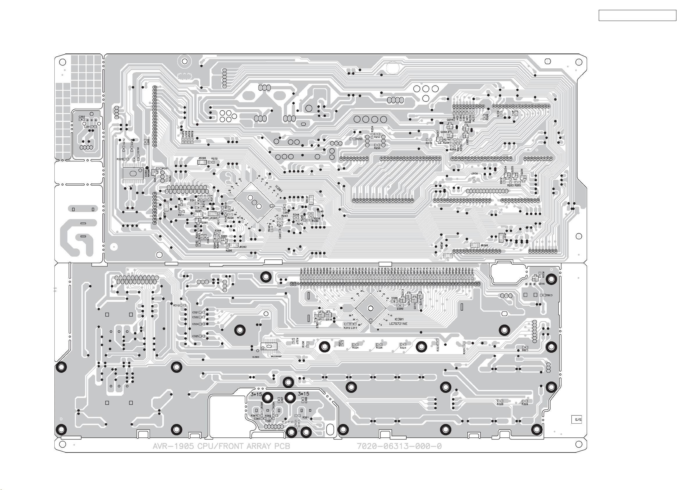
AVR-1905/785 AVC-1590
26
FOIL SIDE
 Loading...