

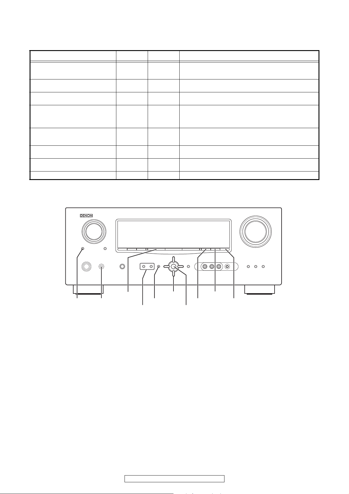
Page 1
Page 2
Please heed the points listed below during servicing and inspection.
SAFETY PRECAUTIONS
The following check should be performed for the continued protection of the customer and service technician.
LEAKAGE CURRENT CHECK
Before returning the unit to the customer, make sure you make either (1) a leakage current check or (2) a line to chassis
resistance check. If the leakage current exceeds 0.5 milliamps, or if the resistance from chassis to either side of the
power cord is less than 460 kohms, the unit is defective.
CAUTION
CAUTION
◎Heed the cautions!
Spots requiring particular attention when servicing, such
as the cabinet, parts, chassis, etc., have cautions indicated
on labels or seals. Be sure to heed these cautions and the
cautions indicated in the handling instructions.
◎Caution concerning electric shock!
(1) An AC voltage is impressed on this set, so touching in-
ternal metal parts when the set is energized could
cause electric shock. Take care to avoid electric shock,
by for example using an isolating transformer and
gloves when servicing while the set is energized, unplugging the power cord when replacing parts, etc.
(2)There are high voltage parts inside. Handle with extra
care when the set is energized.
◎Caution concerning disassembly and
assembly!
Though great care is taken when manufacturing parts from
sheet metal, there may in some rare cases be burrs on the
edges of parts which could cause injury if fingers are
moved across them. Use gloves to protect your hands.
◎Only use designated parts!
The set's parts have specific safety properties (fire resistance, voltage resistance, etc.). For replacement parts, be
sure to use parts which have the same properties. In particular, for the important safety parts that are marked z on
wiring diagrams and parts lists, be sure to use the designated parts.
◎Be sure to mount parts and arrange
the wires as they were originally!
For safety reasons, some parts use tape, tubes or other insulating materials, and some parts are mounted away from
the surface of printed circuit boards. Care is also taken with
the positions of the wires inside and clamps are used to
keep wires away from heating and high voltage parts, so
be sure to set everything back as it was originally.
◎Inspect for safety after servicing!
Check that all screws, parts and wires removed or disconnected for servicing have been put back in their original positions, inspect that no parts around the area that has been
serviced have been negatively affected, conduct an insulation check on the external metal connectors and between
the blades of the power plug, and otherwise check that
safety is ensured.
(Insulation check procedure)
Unplug the power cord from the power outlet, disconnect
the antenna, plugs, etc., and turn the power switch on. Using a 500V insulation resistance tester, check that the insulation resistance between the terminals of the power
plug and the externally exposed metal parts (antenna terminal, headphones terminal, microphone terminal, input
terminal, etc.) is 1MΩ or greater. If it is less, the set must
be inspected and repaired.
Concerning important safety
parts
Many of the electric and structural parts used in the set
have special safety properties. In most cases these properties are difficult to distinguish by sight, and using replacement parts with higher ratings (rated power and
withstand voltage) does not necessarily guarantee that
safety performance will be preserved. Parts with safety
properties are indicated as shown below on the wiring diagrams and parts lists is this service manual. Be sure to replace them with parts with the designated part number.
(1) Schematic diagrams ... Indicated by the z mark.
(2) Parts lists ... Indicated by the z mark.
Using parts other than the designated
parts could result in electric shock, fires or
other dangerous situations.
AVR-1910/1620/1610/790/590
2
Page 3
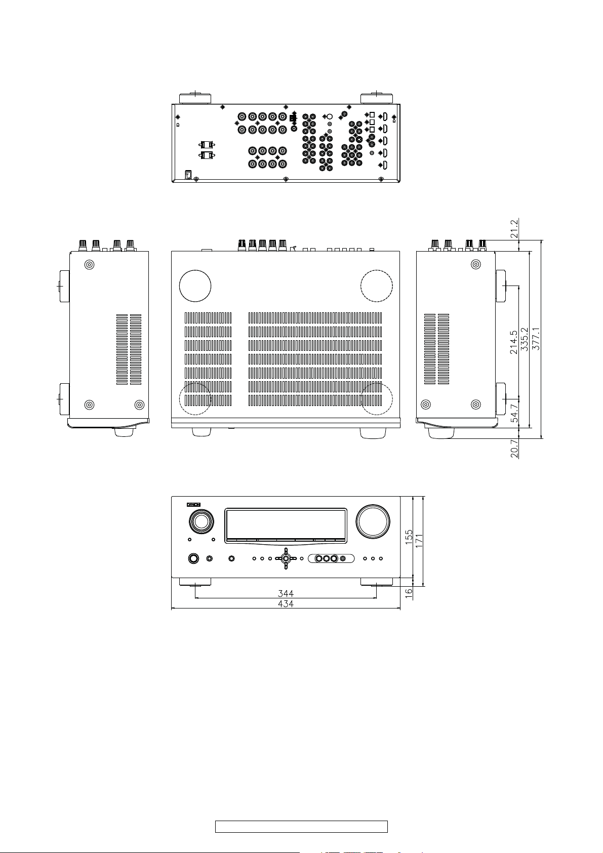
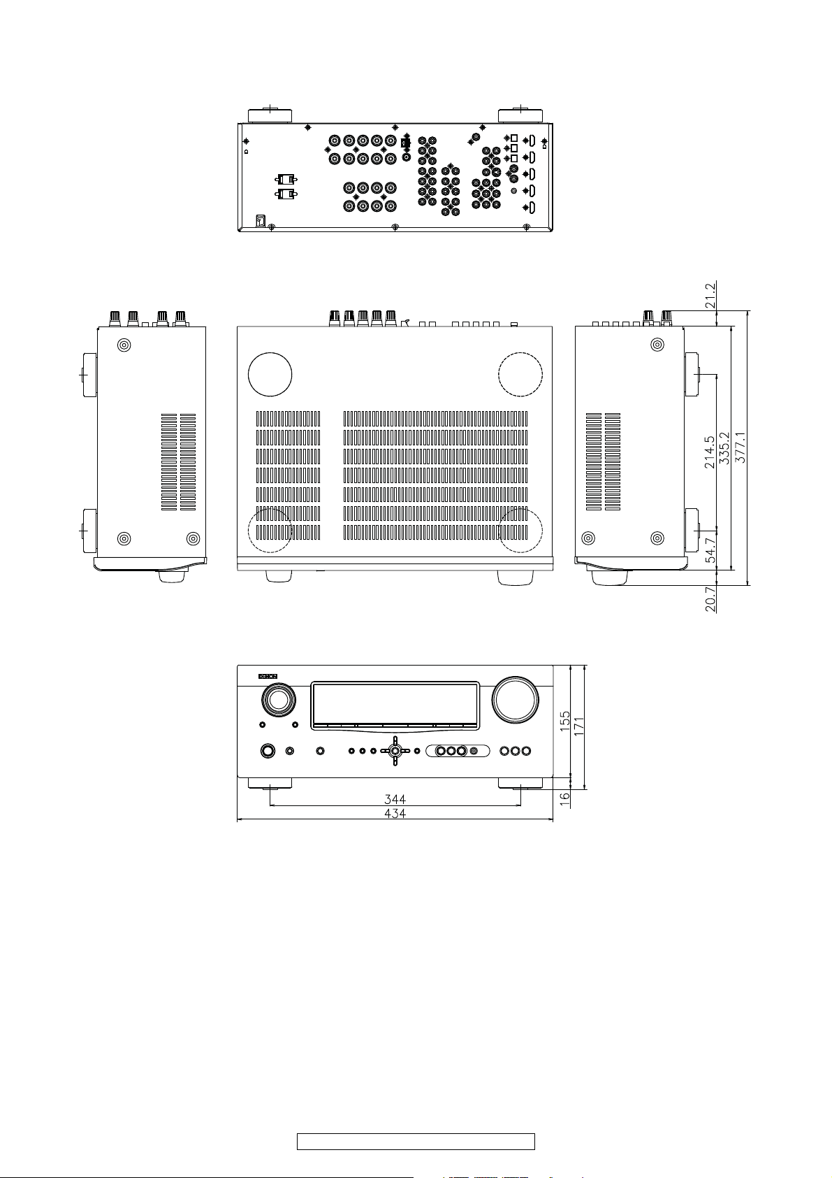
DIMENSION
AVR-1910 model
3
AVR-1910/1620/1610/790/590
Page 4
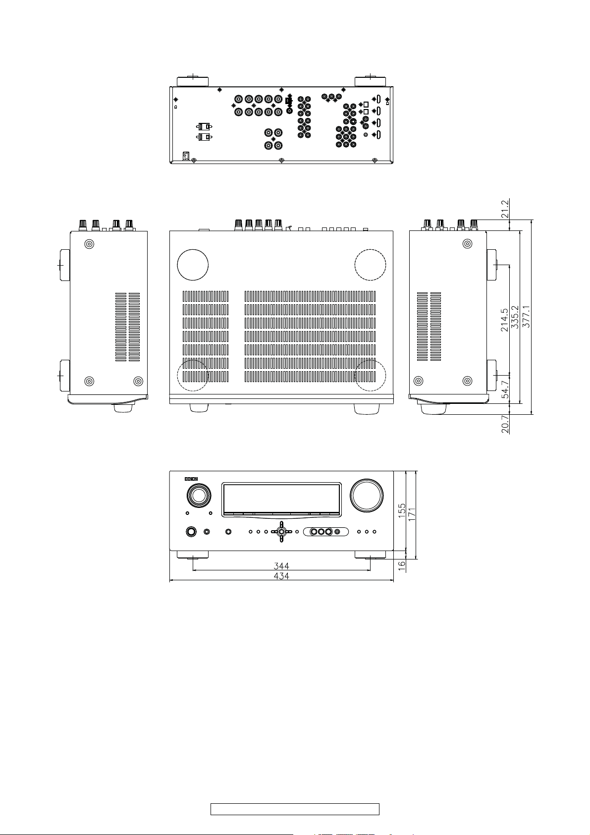
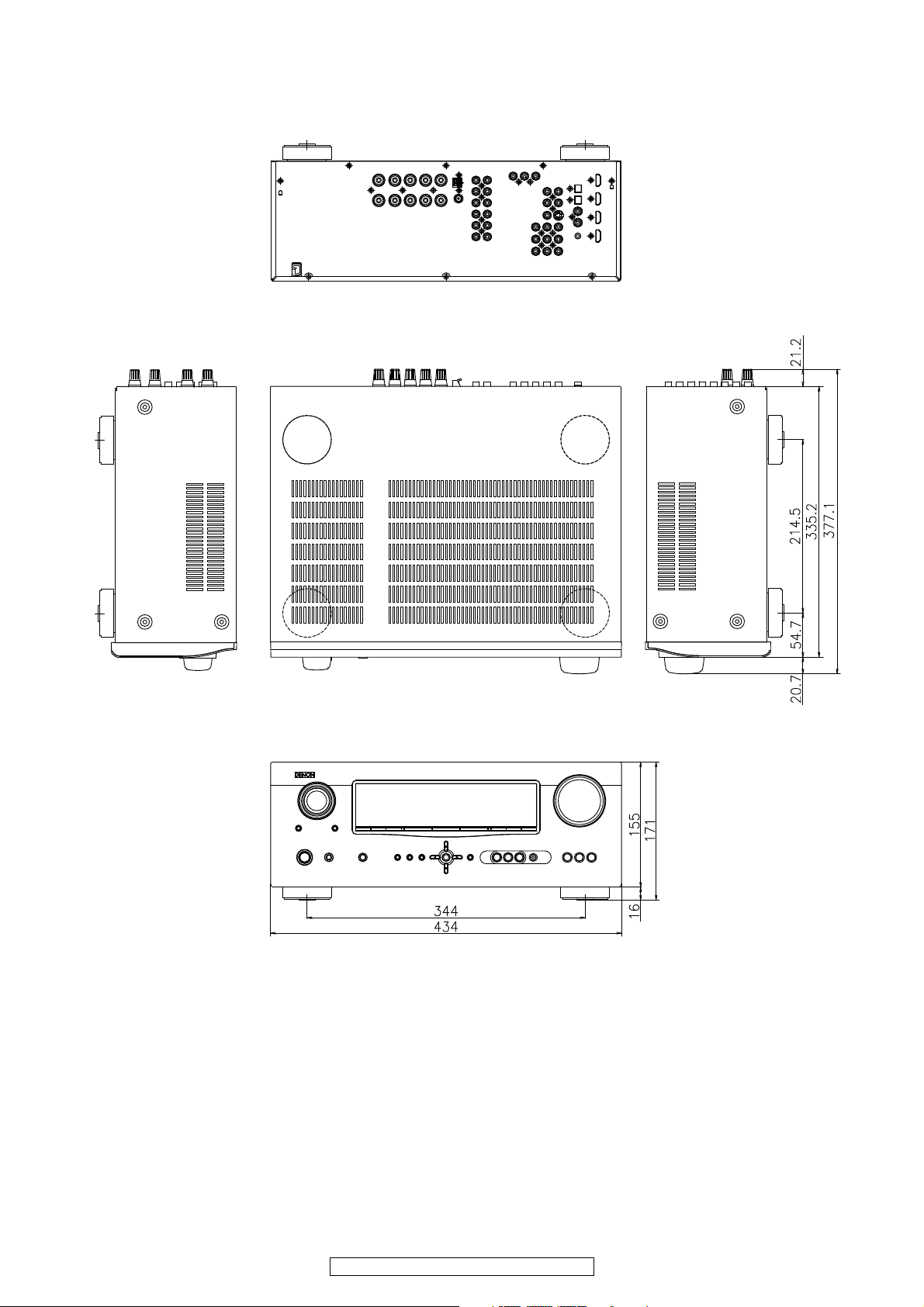
AVR-1610/1620 model
4
AVR-1910/1620/1610/790/590
Page 5
AVR-790 model
5
AVR-1910/1620/1610/790/590
Page 6
AVR-590 model
6
AVR-1910/1620/1610/790/590
Page 7
WIRE ARRANGEMENT
Back Panel side
Front Panel side
If wire bundles are untied or moved to perform adjustment or parts replacement etc., be sure to rearrange them neatly as
they were originally bundled or placed afterward.
Otherwise, incorrect arrangement can be a cause of noise
generation.
Wire arrangement viewed from the top
7
AVR-1910/1620/1610/790/590
Page 8
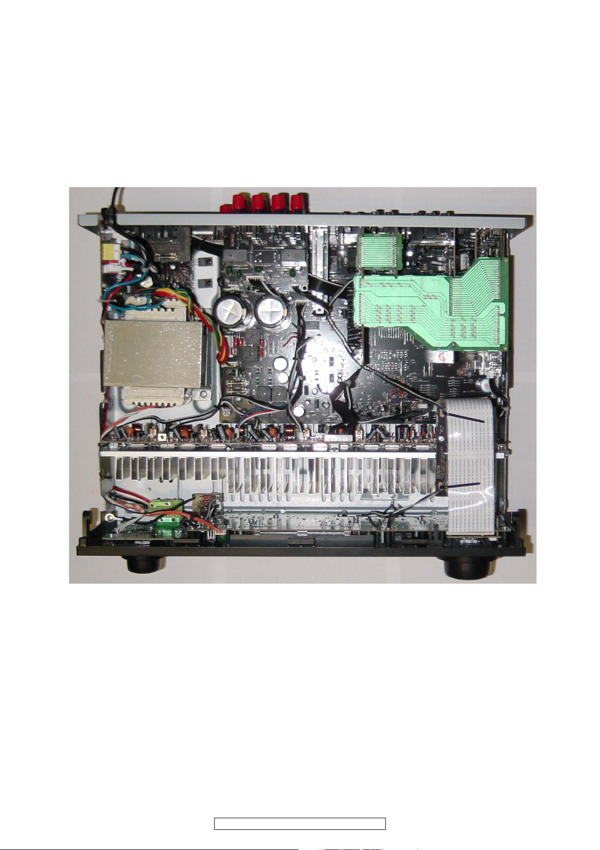
DISASSEMBLY
CABINET TOP
PANEL FRONT ASSY PCB CNT1 PCB SPEAKER ASSY
Refer to "DISASSEMBLY 1.PANEL FRONT ASSY" Refer to "DISASSEMBL 2.PCB CNT1" Refer to "DISASSEMBLY 3.PCB SPEAKER ASSY"
and "EXPLODED VIEW" and "EXPLODED VIEW" and "EXPLODED VIEW"
PCB POWER SW ASSY PCB CNT1 (Ref. No. of EXPLODED VIEW : 71) PCB SPEAKER ASSY
(Ref. No. of EXPLODED VIEW : 9) (Ref. No. of EXPLODED VIEW : 63)
PCB FUNC ASSY
(Ref. No. of EXPLODED VIEW : 10)
PCB FRONT ASSY
(Ref. No. of EXPLODED VIEW : 11)
CHASSIS BACK PCB POWER/POWER SUPPLY ASSY
PCB ENCORDER
Refer to "DISASSEMBLY 4.CHASSIS BACK" Refer to "DISASSEMBLY
(Ref. No. of EXPLODED VIEW : 13) and "EXPLODED VIEW" 6.PCB POWER/POWER SUPPLY ASSY"
PCB HEAD PHONE ASSY
and "EXPLODED VIEW"
(Ref. No. of EXPLODED VIEW : 14) PCB POWER SUPPLY ASSY
PCB V-AUX ASSY (Ref. No. of EXPLODED VIEW : 56)
(Ref. No. of EXPLODED VIEW : 21) PCB POWER ASSY
PCB MIC ASSY
PCB MAIN ASS
Y
(Ref. No. of EXPLODED VIEW : 57)
(Ref. No. of EXPLODED VIEW : 22)
Refer to "DISASSEMBLY 5.PCB MAIN ASSY"
PCB CNT ENCORDER and "EXPLODED VIEW"
(Ref. No. of EXPLODED VIEW : 61) PCB MAIN ASSY
TRANS MAIN
PCB SW (Ref. No. of EXPLODED VIEW : 50)
Referto"DISASSEMBLY8.TRANSMAIN"
(Ref. No. of EXPLODED VIEW : 78) PCB INPUT ASSY and "EXPLODED VIEW"
(Ref. No. of EXPLODED VIEW : 51) TRANS MAIN
PCB VIDEO ASSY (Ref. No. of EXPLODED VIEW : 46)
PCB AMP ASSY (Ref. No. of EXPLODED VIEW : 53)
Refer to "DISASSEMBLY 7.PCB AMP ASSY"
PCB DIGITAL ASSY
and "EXPLODED VIEW" (Ref. No. of EXPLODED VIEW : 54)
PCB AMP ASSY PCB HDMI ASSY
(Ref. No. of EXPLODED VIEW : 33) (Ref. No. of EXPLODED VIEW : 55)
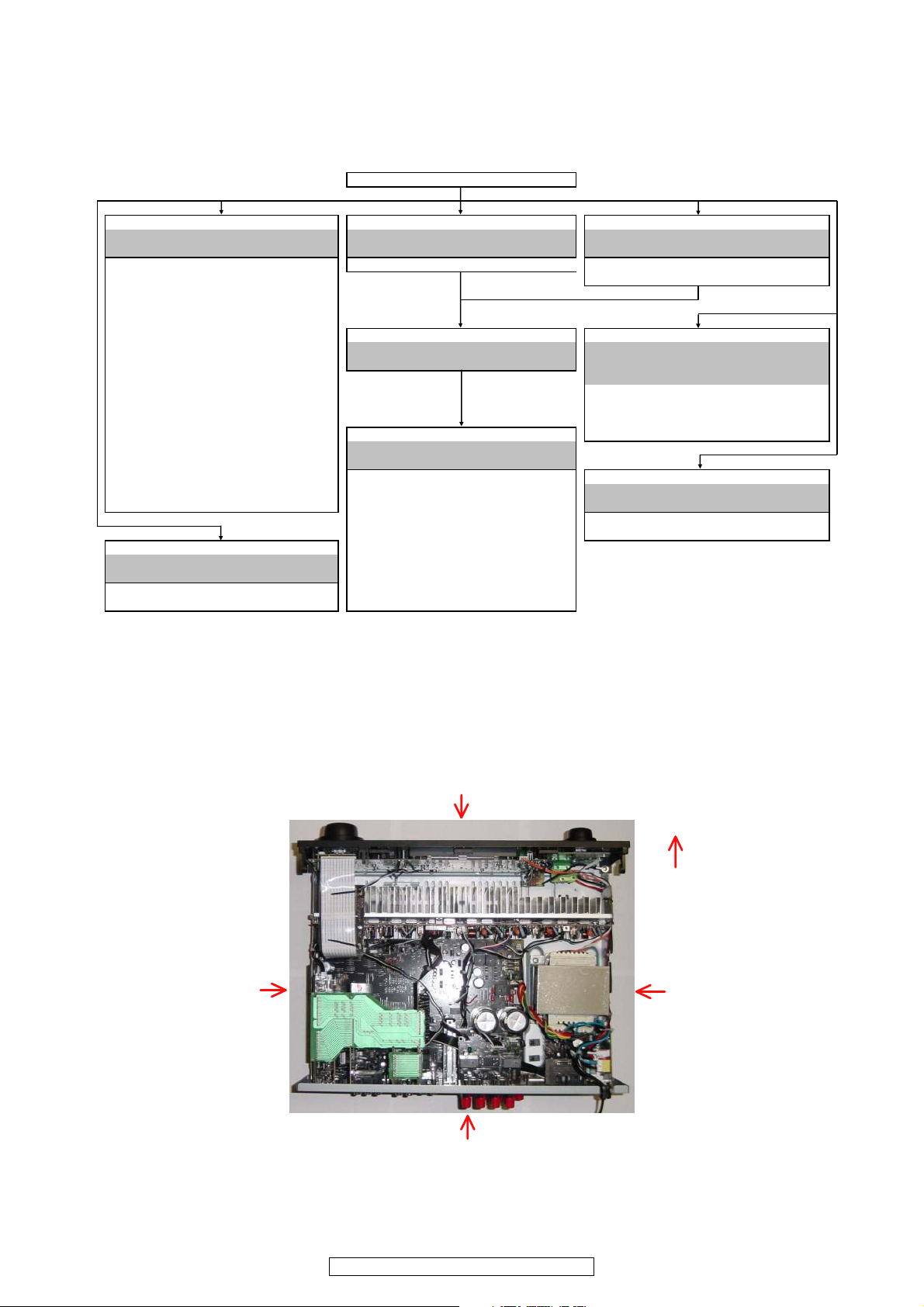
The viewpoint of each photograph
(Photografy direction)
[View from above]
Front side
Direction of photograph: B
Direction of photograph: D
Direction of photograph: C
Direction of photograph: A
• Disassemble in order of the arrow of the figure of following flow.
• In the case of the re-assembling, assemble it in order of the reverse of the following flow.
• In the case of the re-assembling, observe "attention of assembling" it.
About the photos used for descriptions in the “DISASSEMBLY” section.
• The direction from which the photographs used herein were photographed is indicated at "Direction of photograph: ***" at
the left of the respective photographs.
• Refer to the table below for a description of the direction in which the photos were taken.
• Photographs for which no direction is indicated were taken from above the product.
• The photograph is AVR-1910.
8
AVR-1910/1620/1610/790/590
Page 9
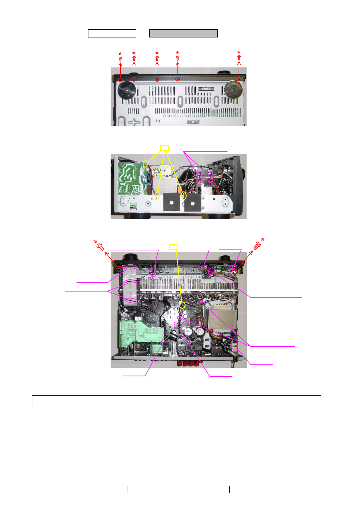
1. PANEL FRONT ASSY
Proceeding : CABINET TOP →PANEL FRONT ASSY
View from bottom
Direction of photograph: D
Style pin : Loose
cut
Cord holder : Loose
Cord holder : Loose
Style pin : Loose
CP1501
CP1300
Style pin : Loose
CP1001
CP1705
FFC Cable
CP1307
cut
Please refer to "EXPLODED VIEW" for the disassembly method of each P.W.B included in PANEL FRONT ASSY.
(1) Remove the screws.
(2) Cut the wire clamp band, and loose the style pin.
(3) Cut the wire clamp band, then loose the style pin and Cord holder. Disconnect the connector wire and FFC Cable.
AVR-1910/1620/1610/790/590
9
Page 10
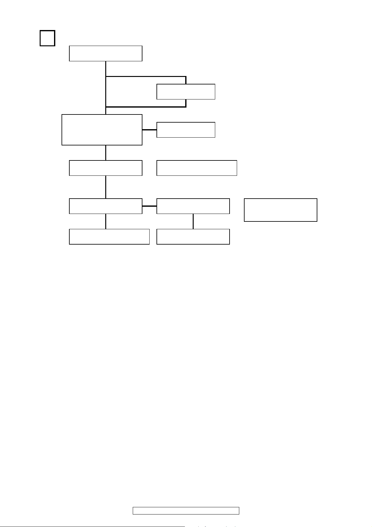
2. PCB CNT1
Proceeding : CABINET TOP →PCB CNT1
PCB CNT1
PCB CNT (1910/790 model)
Board to board
Board to board
Board to board
Proceeding : CABINET TOP →PCB SPEAKER ASSY
CP1001 (1910/790 model)
CN1309 (1910/790 model)
CP1002 (1910/790 model)
※CP1003 (1610/1620/590/ model), CP1004 (1610/1620/590/ model)
PCB SPEAKER ASSY
Direction of photograph: A
(1) Disconnect the connector board.
3. PCB SPEAKER ASSY
(1) Disconnect the connector wires.
(2) Remove the screws.
10
AVR-1910/1620/1610/790/590
Page 11
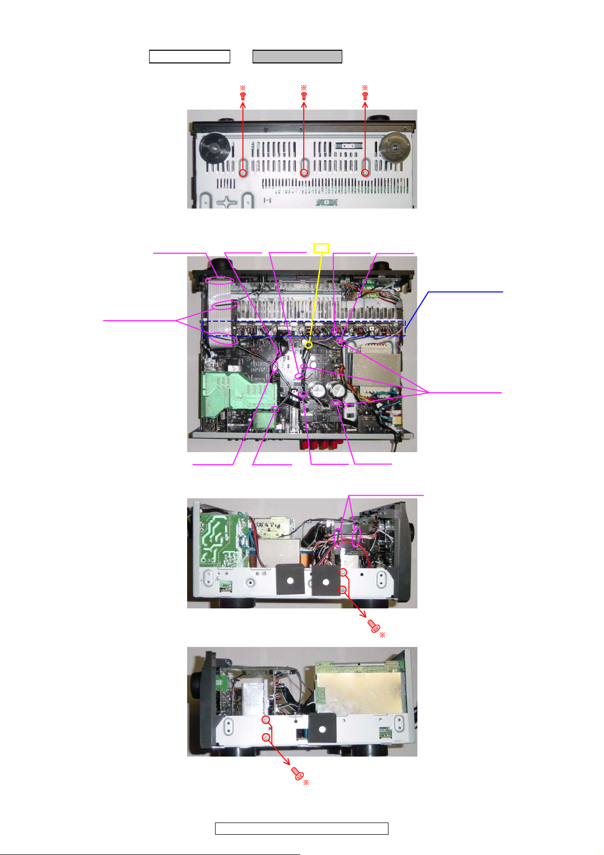
4. CHASSIS BACK
Proceeding : CABINET TOP →PCB SPEAKER ASSY →CHASSIS BACK
Direction of photograph: A
Proceeding : CABINET TOP →PCB SPEAKER ASSY →CHASSIS BACK
→PCB MAIN ASSY
CP1700
CP1002
CP1004
CP1001
CP1003
Style pin : Loose
CP1001
CP1005
CP1501
CP1200
CP1000
CP1003
FFC Cable
Style pin : Loose
cut
cut
(1) Remove the screws.
5. PCB MAIN ASSY
(1) Cut the wire clamp band, then loose the style pin and Cord holder. Disconnect the connector wire and FFC Cable.
11
AVR-1910/1620/1610/790/590
Page 12
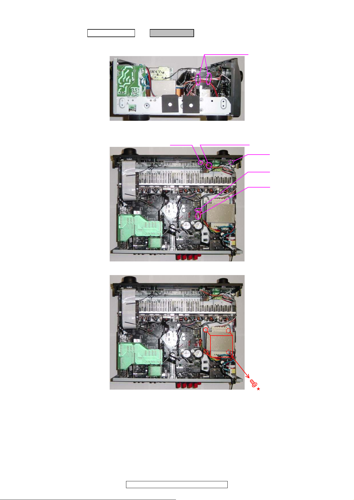
(1) Disconnect the connector board.
Board to board
Board to board
Board to board
PCB DIGITAL ASSY
PCB MAIN ASSY
PCB VIDEO ASSY
PCB EXT. ASSY (1910/790 model) PCB INPUT ASSY
PCB HDMI ASSY
(2) Remove the screws.
AVR-1910/1620/1610/790/590
12
Page 13
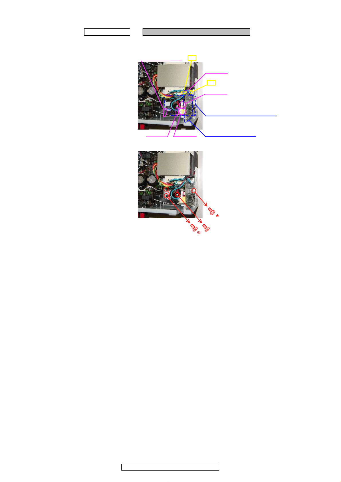
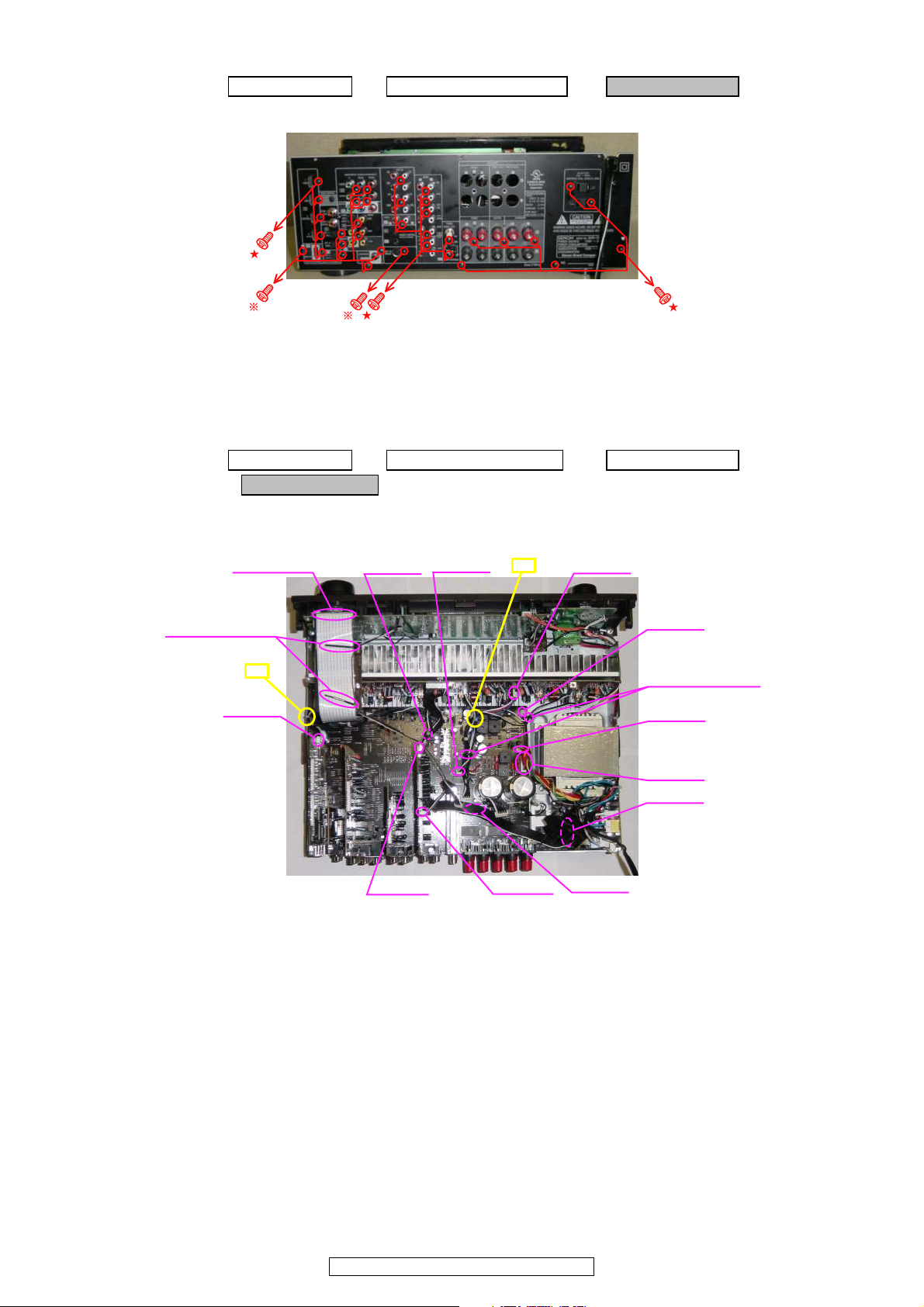
6. PCB POWER/POWER SUPPLY ASSY
Proceeding : CABINET TOP →PCB POWER/POWER SUPPLY ASSY
cut
cut
CP1705
CP1706
CP1704
CP1700
Style pin : Loose
PCB POWER ASSY
PCB POWER SUPPLY ASSY
ً
(1) Cut the wire clamp band, then loose the style pin and Cord holder. Disconnect the connector wire.
(2) Remove the screws.
AVR-1910/1620/1610/790/590
13
Page 14
7. PCB AMP ASSY
Proceeding : CABINET TOP →PCB AMP ASSY
View from bottom
FFC Cable
CP1200
CP1003
Style pin : Loose
Style pin : Loose
CP1005
CP1001
CP1001
CP1000
CP1309
CP1501
cut
PCB AMP ASSY
Direction of photograph: D
Style pin : Loose
Direction of photograph: C
(1) Remove the screws.
(2) Cut the wire clamp band, then loose the style pin and Cord holder. Disconnect the connector wire.
(3) Loose the style pin, then remove the screws.
AVR-1910/1620/1610/790/590
14
Page 15
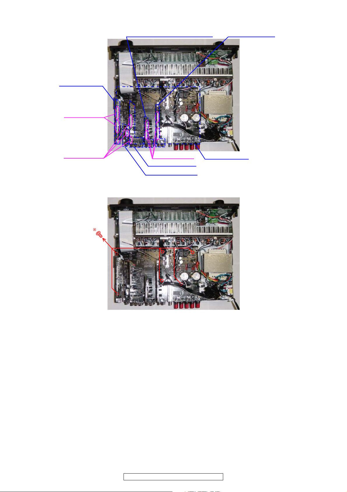
8. TRANS MAIN
Proceeding : CABINET TOP → TRANS MAIN
Direction of photograph: D
Style pin : Loose
CP1002
CP1004
CP1307
CP1300
Cord holder : Loose
(1) Loose the style pin.
(2) Loose the Cord holder, then disconnect the connector wire.
(3) Remove the screws.
AVR-1910/1620/1610/790/590
15
Page 16
CAUTION IN SERVICING
Note:・If step 3 does not work, start over from step 1.
・ All user settings will be lost and this factory setting will be recovered when this initialization mode.
So make sure to m+emorize your setting for restoring after the initialization.
SURROUND
MODE 0
SURROUND
MODE 1
ON/OFF
Initializing AV SURROUND RECEIVER
AV SURROUND RECEIVER initialization should be performed when the µcom, peripheral parts of µcom, and Digital P.W.B.
are replaced.
1. Switch off the unit.
2. With the "SURROUND MODE 0" and "SURROUND MODE 1" buttons pressed, press the "ON/OFF" button to turn the
power on.
3. Check that the entire display is flashing with an interval of about 1 second, and release your fingers from the 2 buttons and
the microprocessor will be initialized.
JIG to use for servicing
When you repair the printing board, you can use the following JIG (Extension cable kit). Please order to Denon Official Service
Distributor in your region if necessary.
00D SPK- 561 EXTENSION UNIT KIT : 1 Set
00D SPK- 562 9120 CONN. JOINT KIT : 1 Set
When you update the firmware, you can use the following
JIG (RS232C to internal connector conversion adapter with 8P cable kit ). Please order to Denon Official Service Distributor
in your region if necessary.
00DSPK-581 WRITING UNIT : 1 Set
AVR-1910/1620/1610/790/590
16
Page 17
SPECIAL MODE g
0
0
DIMMER
STATUSMULTEQ
ENTER
MENU
SURROUND
0 MODE 1
ON/OFF
CURSOR
SOURCE
RESTORER
Special mode setting button
※Press the ON/OFF button to turn on while pressing both buttons A and B at the same time.
Mode Button A Button B Contents
µcom/DSP Version display mode
Errors checking mode
(Displaying the protection history)
Initialization mode
Mode for switching tuner frequency step
Mode for preventing remote control
acceptance
Panel lock mode
Panel lock mode
(Remove Master volume)
Cancellation of panel lock mode MENU RESTORER Panel lock mode is cancelled.
STATUS DIMMER
STATUS MULT EQ
SURROUND
MODE0
SOURCE
CURSOR 0 RESTORER
SURROUND
MODE0
SURROUND
MODE1
SURROUND
MODE1
-
(non)
RESTORER
RESTORER Operations using main unit panel buttons are rejected.
Serial No. and firmware versions such as Main, Sub, DSP are
displayed in the FL manager. Errors are displayed when they
occur. (Refer to 18 page.)
Displaying the protection history
(Refer to 19 page.)
Backup data initialization is carried out.
(Refer to 16 page.)
---E2 model only--Select with the SOURCE 01 button.
Change tuner frequency step to AM9k/FM50kHz STEP or AM:10k/
FM:200kHz.
Operations using remote control are rejected.
(Mode cancellation: Turn off power and execute the same button
operations as when performing setup.)
Operations using main unit panel buttons or master volume are
rejected.
AVR-1910/1620/1610/790/590
17
Page 18
1. µcom/DSP Version display mode
1.1. Operation specifications
µcom/DSP version display mode:
When started up, the version information is displayed.
Starting up:
With the "DIMMER" and "STATUS" buttons pressed, press the "ON/OFF" button to turn the power on.
Now, press the "STATUS" button to the display the 2nd item information on the FL Display.
1.2. Display Order
Destination information →Main-µcom version information →Sub-µcom version information → DSP version information
→ APLD version information
1.3. Error display g
See the following table for each "Error information" display and its contents (status).
Display order is ①②③④.
Condition State Display
①Sub-µcom
NG
②DIR NG
③DSP NG
Both SUB/DSP
④
OK
No response from Sub-µcom
No response from DIR
When DSP boot, executing DSP reset makes no change to DSP FLAG0
port "H".
No change to DSP FLAG0 port "H" before issuing DSP command.
When DSP data read, executing WRITE="L" makes no change to ACK="H".
When DSP data read, executing REQ="L" makes no change to ACK="L".
When DSP data write, executing WRITE="H" makes no change to ACK="H".
When DSP data write, executing REQ="L" makes no change to ACK="L".
When DSP special code boot, executing DSP reset makes no change to
DSP FLAG0 port "H".
No change to DSP FLAG0 port "H" before issuing DSP special read com-
mand.
No change to DSP FLAG0 port "H" before DSP version read.
"□SUB□ □ERROR□01□□"
"□DIR□ □ERROR□01□□"
"□DSP□□ERROR□01□ □"
"□DSP□□ERROR□02□ □"
"□DSP□□ERROR□03□ □"
"□DSP□□ERROR□04□ □"
"□DSP□□ERROR□05□ □"
"□DSP□□ERROR□06□ □"
"□DSP□□ERROR□11□ □"
"□DSP□□ERROR□12□ □"
"□DSP□□ERROR□13□ □"
(No error display, version display
only)
18
AVR-1910/1620/1610/790/590
Page 19
2. Errors checking mode (Displaying the protection history)
2.1. Operation specifications
Error mode (Displaying the protection history):
When started up, the error information is displayed.
Starting up:
●All model commonness
With the "STATUS" and "MULTEQ" buttons pressed, press the "ON/OFF" button to turn the power on. The error (protection
history display) mode is set.
Now, press the "STATUS" button to turn on the FL display.
2.2. About the display on the FL display
When the "STATUS" button is pressed after setting the error (protection history display) mode, a history like the one shown
below is displayed, depending on the conditions.
(1) Normally (when there has been no protection incident)
FLD N O P R O T E C T
(2) For ASO/DC (when the last protection incident was ASO or DC protection)
FLD P R T : A S O / D C
(3) For THERMAL (when the last protection incident was THERMALprotection)
FLD P R T : T H E R M A L
When the "STATUS" button is pressed again after the above protection history is displayed, the normal display reappears.
2.3. Clearing the protection history
There are two ways to clear the protection history, as described below.
(1) Start up the error (protection display) mode, display the error, then press and hold in the "ENTER" button for 3 seconds.
FLD : T H E R M A L T H E
Press and hold in the "ENTER" button for 3 seconds
FLD P R T : C L E A R
The above is displayed and the protection history is cleared.
FLD
(2) Initialize.
※If you want to save a backup, use the method in 3.(1) above.
NO PROT E C T
Warning indication by the POWER LED
If the power is turned off when a protection incident has been detected, the POWER LED (red) flashes as a warning according to the conditions in which the protection incident occurred.
(1) ASO/DC PROTECTION : Flashes in cycles of 0.5 seconds (0.25 seconds lit, 0.25 seconds off)
(2) THERMAL PROTECTION : Flashes in cycles of 2 seconds (1 second lit, 1 second off)
19
AVR-1910/1620/1610/790/590
Page 20

ADJUSTMENT
5CH AMP UNIT (1610/1620/590 model)
7CH AMP UNIT (1910/790 model)
7CH AMP UNIT (1910/790 model)
DC Voltmeter
F Lch
S Lch
C ch
S Rch
F Rch
S Back Lch
S Back Rch
T1201FL
T1201SL
V1201FL
V1201SL
T1201C
V1201C
T1201SR
V1201SR
T1201FR
V1201FR
T1201SBL
V1201SBL
T1201SBR
V1201SBR
Audio Section
Idling Current
Required measurement equipment: DC Voltmeter
1. Preparation
(1) Avoid direct blow from an air conditioner or an electric fan, and adjust the unit at normal room temperature
15 °C ~ 30 °C (59 °F ~ 86 °F).
(2) Presetting
• POWER (Power source switch) OFF
• SPEAKER (Speaker terminal) No load
(Do not connect speaker, dummy resistor, etc.)
2. Adjustment
(1) Remove top cover and set VR1201 FL, FR, C, SL, SR, SBL, SBR on 7CH AMP UNIT at fully counterclockwise (c)
position(1910/790 model).
(1’) Remove top cover and set VR1201 FL, FR, C, SL, SR on 5CH AMP UNIT at fully counterclockwise (c) position(1610/
1620/590 model).
(2) Connect DC Voltmeter to test points (FRONT-Lch: TP1201, FRONT-Rch: TP1205, CENTER ch: TP1203, SUR-
ROUND-Lch: TP1202, SURROUND-Rch: TP1204, SURROUND-BACK Lch: TP1207(1910/790 model), SURROUNDBACK Rch: TP1206 (1910/790 model)).
(3) Connect power cord to AC Line, and turn power switch "ON".
(4) Presetting.
MASTER VOLUME : "---" counterclockwise (c min.)
SPEAKER (Speaker terminal) : No load
(Do not connect speaker, dummy resistor, etc.)
MODE : 7CH STEREO (5CH STEREO)
FUNCTION : CD
(5) Within 2 minutes after the power on, turn VR1201 clockwise (x) to adjust the TEST POINT voltage to 1.5 mV ± 0.5 mV
DC.
(6) After 10 minutes from the preset above, turn VR1201 to set the voltage to 2.0 mV ± 0.5 mV DC.
(7) Adjust the Variable Resistors of other channels in the same way.
20
AVR-1910/1620/1610/790/590
Page 21
TROUBLE SHOOTING
1. POWER
1.1. Power not turn on
Power not turn on
YES
Is the ON/STANDBY indicator on the front panel flashing
red?
YES
Is the fuse blown?
YES
Does the power turn on when
the POWER switch is turned
off then back on?
YES YES YES
Check the primary circuitry
parts including the POWER
switch (for poor contacts,
etc.), and replace any defective parts.
Are there any incomplete
connections in the connec-
NO
tors connecting between the
various circuit boards?
YES YES
Connect the connectors
properly.
NO
NO
Refer to Fuse is blown
Is a DC 5V voltage being
supplied from the POWER
B’D (CN1701 pin 4) to the
microprocessor?
Check the microprocessor
periphery circuitry and
replace any defective parts.
Is there a short circuit
NO
between the speaker terminals and the ground?
Check for damage in the
power amplifier circuitry parts
and replace any defective
parts.
Is a DC 5V voltage output
when the cord supplying the
NO
power from the SUPPLY B’D
to the microprocessor
(CP1700) is unplugged?
Check the circuitry and parts
from CP1700 on the SUPPLY B’D to the microprocessor for damage and shortcircuits, and replace any
defective parts.
Correct the short circuit
NO
between the speaker and
the ground.
Check the parts from
IC1703 to the primary cir-
NO
cuitry and replace any
defective parts.
1.2. Fuse is blown
YES YES YES
Check for leaks or short circuits in the primary side
parts, and replace any defective parts.
YES YES YES
Fuse is blown
Check for short circuits in the
rectifier diodes and circuitry
of the secondary side rectifying circuits, and replace any
defective parts.
After repairing, also replace the fuse.
Check for short circuits in the
power stabilizer unit's regulator output terminal and the
ground, and replace any
defective parts.
21
AVR-1910/1620/1610/790/590
Page 22
2. Analog video
※
※
MONITOR OUT (CVBS/COMPONENT) output NG
When checking operation, select
VCR for the function.
DVR MONITOR OUT(CVBS) Output NG
C
Input
CVBS/S
B
Input
COMPONENT
Input
CVBS/S
When checking operation, select
VCR for the CVBS/S and select
DVD for the COMPONENT.
A
2.1. MONITOR OUT (CVBS/COMPONENT) output NG
DVR MONITOR OUT (CVBS) output NG
AVR-1910/1620/1610/790/590
22
Page 23
Input S
Input CVBS
OK
OK
Check V±5V,4094_PWR(+5V)
OK
Check input selector and
surrounding circuitry soldering.
Output V:
IC1901 24pin
Input V:
Check output of input selector.
To troubleshooting 1.1
Power not turn on.
+5V:
CN1018 3pin
Check connection of
iPod Doc.
Check input of VIDEO buffer.
Check surrounding circuitry
soldering of OSD IC.
Check input of OSD IC.
Input V:
IC1905 17pin
IC1901 12pin
OK
NG
Check input selector and
surrounding circuitry soldering.
Input
COMPONENT
V±5V
NG
OK
A
Input
CVBS or S
-5V:
CN1018 4pin
4094_PWR(+5V):
-5V:
CN1018 4pin
To troubleshooting 1.1
Power not turn on.
NG
CN1018 3pin
+5V:
B
Check output of input selector. NG
Output V:
IC1906 3pin
Check output of VIDEO buffer.
IC1905 13pin
NG
Check cable between main unit
and monitor or check monitor.
OK
CN1018 1pin
Check output of VIDEO buffer
(IC19000A) and surrounding
circuitry soldering.
Check output of VIDEO buffer
(IC1904B) and surrounding
circuitry soldering.
NG
OK
NG
NGCheck output of OSD IC.
Output V:
OK
Check cable between main unit
and monitor or check monitor.
IC1907 24pin
IC1907 22pin
IC1907 20pin
Output Y:
Output Cb:
Output Cr:
Check surrounding circuitry
soldering of VIDEO buffer.
AVR-1910/1620/1610/790/590
23
Page 24
Input S
Input CVBS
-5V:
OK
Check surrounding circuitry
soldering of VIDEO buffer.
OK
Check output of VIDEO buffer
(IC1904B) and surrounding
circuitry soldering.
Output V:
IC1901 33pin
Input V:
IC1901 3pin
OK OK
Check input selector and
surrounding circuitry soldering.
Output V:
IC1906 3pin
Check output of VIDEO buffer. NG Check input of VIDEO buffer. NG
Check output of input selector. NG
C
Input
CVBS/S
CN1018 3pin
4094_PWR(+5V):
+5V:
Check connection of
iPod Doc.
To troubleshooting 1.1
Power not turn on.
CN1018 4pin
NG
Check V±5V,4094_PWR(+5V)
CN1018 1pin
Check cable between main unit
and monitor or check monitor.
24
AVR-1910/1620/1610/790/590
Page 25
2.2. HDMI OUT Output NG (AVR-1910/790 model)
※
HDMI OUT output NG
Input
CVBS
Input
S
When checking operation, select
DVD for the function.
(COMPONENT1 input)
Input
COMPONENT
Input
HDMI
To troubleshooting
HDMI/DVI.
D
25
AVR-1910/1620/1610/790/590
Page 26
OK
※
D
+5V:
CN1018 3pin
Check connector base
soldering of CNT 1 B'D and
incomplete connection of B'D.
To troubleshooting HDMI/DVI.
Unless specified, HDMI B'D part.
OK
Input Cb:
Input Cr:
CN1102 7pin
CN1102 9pin
Input
CVBS/S/OMPONENT
OK
HDMI B'D
Check input of video decoder signal.
To troubleshooting 1.1 Power not
turn on.
Check output of CVBS VIDEO buffer
(IC1900A) of VIDEO B'D and
COMPONENT input selector (IC1907
24,22,20pin).
NG NG
To A or B
Input V:
Input Y:
CN1102 3pin
CN1102 5pin
+1.8V:
L3 and L4
OK
CN1018 4pin
-5V:
CN1018 1pin
4094_PWR(+5V):
NG
To troubleshooting 1.1
Power not turn on.
OK
NG
Check of power supply voltage .
+3.3V:
Emitter side of Q24 and L2
Check surrounding circuitry
soldering of IC19, IC29 and IC35.
Check of power supply voltage
(VIDEO B'D).
26
AVR-1910/1620/1610/790/590
Page 27
3. HDMI/DVI
3.1. No picture or sound is output
No picture or sound is output
Check the HDMI/DVI cable
connection
Is the HDMI/DVI cable properly
connected?
Are you using an HDMI/DVI
selector, repeater or a device
for improving picture quality?
Are you using a certified HDMI
cable (one with the HDMI
stamp)?
Are you using an HDMI/DVI
cable less than 5 meters in
length?
YES
YES
YES
NO
YES
There may be a problem with
NO
the HDMI/DVI cable. Check the
connection.
Disconnect everything and
YES
connect only the HDMI/DVI
cable to check.
Use a certified HDMI cable
NO
(one with the HDMI stamp).
Replace the HDMI/DVI cable
with one that is less than 5
NO
meters in length (2 meters
recommended) to check.
YES
Are the picture and sound
output when another HDMI/DVI
cable is used?
NO
Checking the DVD player
YES
Is the DVD player's HDMI
output setting correct?
YES
When using a DENON DVD player, is the fluorescent display tube's
"HDMI" indicator lit?
If using a non-DENON DVD player, proceed to "YES".
YES
Are the picture and sound
NO
Is sound output from the set's speaker terminals when the TV's power is
turned off or the connection cable between the TV and the set is
disconnected?
output when the DVD player's
resolution is changed?
NO
The HDMI/DVI cable is
YES
defective.
Check the HDMI output setting,
YES
referring to the DVD player's
operating instructions.
Set the DVD player's output
YES
resolution to a resolution with
which the TV is compatible.
The DVD player may not be
compatible with HDCP
YES
repeaters. Ask the DVD
player's manufacturer.
NO
Are the picture and sound
output when a different DVD
player is used?
NO
27
AVR-1910/1620/1610/790/590
YES
The DVD player is defective.
Page 28
Check the TV
Is the TV HDCP-compatible?
YES
Is the TV compatible with resolutions of 1080P?
YES
Is the TV's input set to HDMI?
YES
Use an HDCP-compatible TV.
NO
PC TVs cannot be used.
If the TV is not compatible with
resolutions of 1080P, no picture
NO
will be output, even if the DVD
player's resolution is set to
1080P.
Check the TV's input setting,
NO
referring to the TV's operating
instructions.
Are the picture and sound output when a different TV is used?
YES
Check the set (AVR-4310CI)
Is the set's input set to HDMI?
YES YES
The set does not recognize the TV.
Is the TV information properly displayed on the "Monitor info." display
menu?
Is IC5 pin 3 "H" (3V-5V)? With the TV connected, check the voltage of
the IC on the side on which the TV is connected.
YES
The DVD player does not
recognize the connection
When using a DENON DVD
player, is the fluorescent
display tube's "HDMI" indicator
lit?
If using a non-DENON DVD
player, proceed to "NO".
with the set.
Is the HDMI connector (JACK1/
NO
JACK2/JACK3/JACK4) pin 19
"H" (5V)? With the DVD player
connected, check the voltage
of the HDMI connector for the
input on the side on which the
DVD player is connected.
NO
The TV is defective.
Check the set's input setting,
NO
referring to the set's operating
instructions.
The pattern and circuit from
the HDMI connector (JACK5)
to the IC (IC5) is defective, or
NO
the HDMI output circuitry is
defective.
(IC5/IC31 and surrounding
circuitry)
The pattern and circuit from
the HDMI connector (JACK1/
NO
JACK2/JACK3/JACK4) to the
IC1045 is defective.
YES YES
The HDMI output circuitry is defective.
(IC1/IC31/IC5 and surrounding circuitry)
28
AVR-1910/1620/1610/790/590
Page 29
BLOCK DIAGRAM
AUDIO BLOCK DIAGRAM
29
AVR-1910/1620/1610/790/590
Page 30
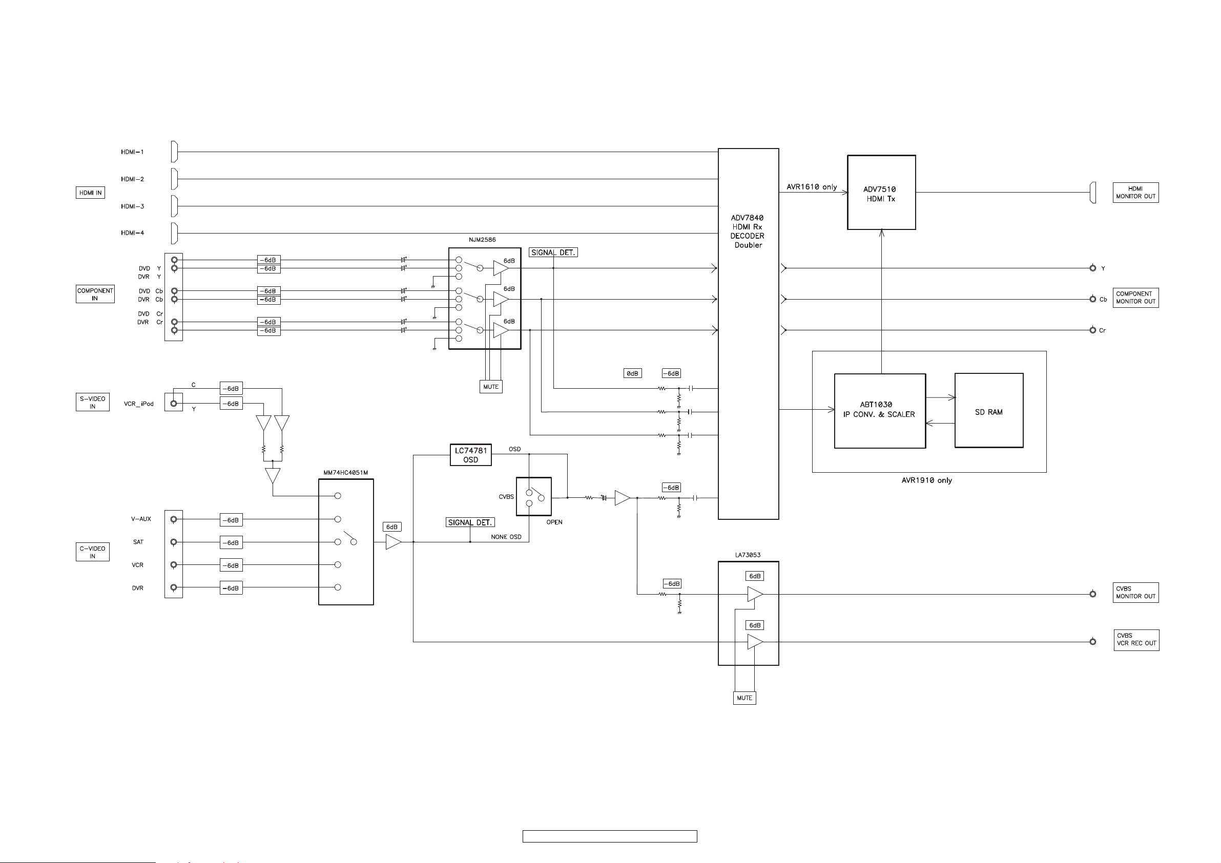
VIDEO BLOCK DIAGRAM
30
AVR-1910/1620/1610/790/590
Page 31

VCC DIAGRAM
S4(VIDEO)
S1(AMP +B)
S5(-VKK)
S6(FILAMENT)
MAIN TRANS
S3(DSP.HDMI)
S2(+12V,-12V)
AVR1910 ONLY
SUB TRANS
AC CORD
AC OUTLET
AVR1910 ONLY
31
AVR-1910/1620/1610/790/590
Page 32

LEVEL DIAGRAMS
F$
F$
F$
&52
F$
010%.+%2/#:5+)0#..'8'.8TOU
%QPHKIޓ&1.$;.+/+6.'8'.8TOU#..EJF$(5
F$
57/(41/59EJ
%QPHKIޓ&1.$;.+/+6.'8'.#..EJF$(5
8
FRONT LEVEL DIAGRAM
4#(2
LEVEL DIAGRAM
FRONT ch
#0#.1)
#66
*2176
.+0'+0
#8410.;
':6+0
F$
F$
ޓF$
O8
F$
F$
㧗
㧗
.+0'+0':6+0#845GTKGU
#8410.;
61
5WTTQWPF$CEM
<10'/1&'
㧗㧙
㧗
)#+0
#&,
#&
#
F$(5&+)+0
2%/QT&&%QPHKI
F$(5#&+0
F$(5&+)+0
ޓ&&%QPHKI
&#
F$(5
8TOU
F$(5
F$(5
F$(5
F$(5
㧙
(41/59EJ
F$
㧙
°
/76'
㧗
㧙
㧙
F$
㧙
#
F$(5
F$(5
F$(5
#&+0
O8TOU
F$(5
52'#-'4
4'%176
F$
52176
8TOUǡ
F$
F$
4'%176
ޓF$
*2176
O8TOU
F$
F$
176
F$
F$
F$(5
F$(5
F$
F$
32
AVR-1910/1620/1610/790/590
Page 33

CENTER LEVEL DIAGRAM
F$
F$
F$
010%.+%2/#:5+)0#..'8'.8TOU
%QPHKIޓ&1.$;.+/+6.'8'.#..EJF$(5
F$
%QPHKIޓ&1.$;.+/+6.'8'.#..EJF$(5
&52
LEVEL DIAGRAM
CENTER ch
4#(2
#8410.;
':6+0
F$
F$
O8
ޓF$
F$
F$
㧗
':6+0#845GTKGU
㧗
㧗
#&
㧙
#
F$(5&+)+0
2%/QT&&%QPHKI
F$(5#&+0
F$(5&+)+0
ޓ&&%QPHKI
F$(5
8TOU
&#
F$(5
F$(5
F$(5
F$(5
㧗
F$
㧙
°
/76'
)#+0
#&,
52'#-'4
F$
52176
8TOUǡ
F$
F$
ޓF$
F$
F$
176
F$
F$
F$(5
F$
F$
33
AVR-1910/1620/1610/790/590
Page 34

SUB WOOFER LEVEL DIAGRAM
F$
2.&
&52
010%.+%2/#:5+)0#..'8'.8TOU
%QPHKIޓ&1.$;.+/+6.'8'.#..EJF$(5
F$
%QPHKIޓ&1.$;.+/+6.'8'.ޓ#..EJF$(5
8
57/VQ(4106EJ
LEVEL DIAGRAM
SUBWOOFER ch
4#(2
#8410.;
':6+0
F$
F$
ޓF$
O8
F$
F$
F$
㧗
':6+0#845GTKGU
㧗
#&
#
㧙
F$(5
8TOU
F$(52%/+0
F$(5#&+0
F$(5&+)+0
ޓ&&%QPHKI
&#
#
F$(5
F$(5
F$(5
F$(5
F$(5
㧙
)#+0
㧗
F$
㧙
㧙㧙㧙
F$
°
/76'
F$
57/VQ(4106EJ%QPHKI
#&,
F$
F$
F$
24'176
O8TOU
ޓF$
24'176
O8TOU
F$
F$
F$
24'176/76'
F$
F$(5
F$
34
AVR-1910/1620/1610/790/590
Page 35

SURROUND LEVEL DIAGRAM
F$
F$
F$
010%.+%2/#:5+)0#..'8'.8TOU
%QPHKIޓ&1.$;.+/+6.'8'.8TOU#..EJF$(5
F$
%QPHKIޓ&1.$;.+/+6.'8'.8TOU#..EJF$(5
&52
LEVEL DIAGRAM
SURROUND ch
4#(2
':6+0
#8410.;
㧗
F$
F$
㧗
㧗
#&
㧙
#
F$(5
8TOU
&#
F$(5
㧗
㧙
°
/76'
)#+0
#&,
52'#-'4
F$
52176
8TOUǡ
F$
F$
176
O8
':6+0#845GTKGU
ޓF$
F$
F$
F$
F$
F$(5
F$(5&+)+0
2%/QT&&%QPHKI
F$(5#&+0
F$(5&+)+0
ޓ&&%QPHKI
F$(5
F$(5
F$(5
F$
35
AVR-1910/1620/1610/790/590
ޓF$
F$
F$
F$
F$
Page 36

SURROUND BACK LEVEL DIAGRAM (1910/790 model)
F$
F$
F$
010%.+%2/#:5+)0#..'8'.8TOU
%QPHKIޓ&1.$;.+/+6.'8'.8TOU#..EJF$(5
F$
%QPHKIޓ&1.$;.+/+6.'8'.8TOU#..EJF$(5
F$
&52
LEVEL DIAGRAM
SURR.BACK ch
4#(2
#8410.;
':6+0
O8
F$
F$
':6+0#845GTKGU
ޓF$
F$
F$
F$
㧗
㧗
#&
㧙
㧗
#
F$(5#&+0
F$(5&+)+0
&&':%QPHKI
F$(5&+)+0
&&':%QPHKI
&#
F$(5
8TOU
F$(5
F$(5
F$(5
F$(5
F$(5
㧗
F$
㧙
°
/76'
)#+0
#&,
52'#-'4
176
F$
52176
8TOUǡ
52176°
8TOUǡ
F$
F$
ޓF$
F$
F$
F$
F$
F$
36
AVR-1910/1620/1610/790/590
Page 37

SURROUND BACK LEVEL DIAGRAM (1610/1620/590 model)
F$
010%.+%2/#:5+)0#..'8'. 8TOU
%QPHKIޓ&1.$;.+/+6.'8'.8TOU#..EJF$(5
F$
%QPHKIޓ&1.$;.+/+6.'8'.8TOU#..EJF$(5
F$
&52
LEVEL DIAGRAM
SURR.BACK ch
4#(2
24'176
O8
F$
F$
ޓF$
F$
F$
F$
':6+0
㧗
#&
㧙
#
F$(5#&+0
F$(5&+)+0
&&':%QPHKI
F$(5&+)+0
&&':%QPHKI
&#
F$(5
8TOU
F$(5
F$(5
F$(5
F$(5
F$(5
㧗
F$
㧙
°
/76'
)#+0
#&,
F$
52176°
8TOUǡ
F$
ޓF$
24'176
O8TOU
24'176°
O8TOU
F$
F$
F$
F$
F$
37
AVR-1910/1620/1610/790/590
Page 38

CLOCK FLOW & WAVE FORM IN DIGITAL BLOCK
Wave form
1
CH1: D-DATA
2
CH1: DATA
CH2: fs
CH3: 64fs
3
CH1: DATA
INPUT
㽲
(V.AUX) 1RIDATAD)44()12(ATADR
LC89058W-E
XR)2(1-LAIXAOC 0
(4)RX2 CRLS)34()32(KCRLSK
XR)5(1-LACITPO 3
XR)6(2-LACITPO 4 IDsf652)73()61(KCMRR
(7)RX5 IDsf46)43()71(KCBRR
XR)8(3-LACITPO 6
(1)RXOUT TBCK(45)
DIR/DIT
IC14
㽳
)42(NIDS2-LAIXAOC
RLRCK(20) (42)fsDIR
TMCK(44)
TLRCK(46)
TDATA(47)
GND
CBS)33()22(KCBS K
(F3)HRMCK
HRMCK(19)
(B1)HR64fs/DCLK
HR64fs/DCLK(20)
IC1
HDMI Rx
ADV7840
(A2)HRfs/DR0
(K3)HRSD0/DL0
HRfs/DR0(21)
HRSD0/DL0(22)
(J4)HRSD3/DR2
(D5)HRSD1/DR1
(J3)HRSD2/DL1
HRSD2/DL1(25)
HRSD3/DR2(27)
HRSD1/DR1(23)
IC102
AUDIO PLD
EPM3032ATC
(B2)HRSPDIF/DL2
CH2: fs
CH3: 64fs
CH4: 256fs
ADC/DAC
IC13
ADAU1328
ABCLK(21)
ALRCK(22)
ASDATA(20)
DSDDATA4(11)
DSDDATA3(14)
DSDDATA2(15)
DSDDATA1(16)
DBCLK(17)
DLRCK(18)
38
AVR-1910/1620/1610/790/590
㽴
sf652CAD)53()2(IKLCM
DAC_FL/FR(133)
DAC_C/SW(134)
DAC_SL/SR(135)
(6)DSPIN64fs
(146)
IC204
DSP
ADSP-21367
DAC_SBL/SBR(136)
(8)DSPINfs
(144)
(10)DSPINSB
(132)
(2)DSPINS
(131)
(12)DSPINC
(130)
(13)DSPINF
(125)
(3)DSPOUTfs
(143)
(5)DSPOUT64fs
(137)
Page 39

SEMICONDUCTORS
1 2 3 4 5 6 7 8 9101112131415161718192021222324252627282930
31
32
33
34
35
36
37
38
39
40
41
42
43
44
45
46
47
48
49
50
515253545556575859606162636465666768697071727374757677787980
81
82
83
84
85
86
87
88
89
90
91
92
93
94
95
96
97
98
99
1
00
P0_0/AN0_0/D0
P0_1/AN0_1/D1
P0_2/AN0_2/D2
P0_3/AN0_3/D3
P0_4/AN0_4/D4
P0_5/AN0_5/D5
P0_6/AN0_6/D6
P0_7/AN0_7/D7
8D/0_1P
9D/1_1P
01D/2_1P
11D/3_1P
21D/4_1P
VREF
AVSS
1CCV
NIX
TUOX
SSV
RESET
SSVNC
P8_7/XCIN
TUOCX/6_8P
ETYB
)-/0D/(0A/0_2NA/0_2P
)0D/1D/(1A/1_2NA/1_2P
)1D/2D/(2A/2_2NA/2_2P
)2D/3D/(3A/3_2NA/3_2P
)3D/4D/(4A/4_2NA/4_2P
)4D/5D/(5A/5_2NA/5_2P
)5D/6D/(6A/6_2NA/6_2P
)6D/7D/(7A/7_2NA/7_2P
P3_0/A8(/-/D7)
9A/1_3P
01A/2_3
P
11A/3_3P
21A/4_3P
31A/5_3P
41A/6_3P
51A/7_3P
61A/0_4P
71A/1_4P
81A/2_4P
91A/3_4P
P7_4/TA2OUT/W
TUO3AT/6_7P
P5_6/ALE
P7_7/TA3IN
P5_5/HOLD
P5_4/HLDA
P5_3/BCLK
P5_2/RD
2CCV
VSS
P5_7/RDY/CLKOUT
P4_5/CS1
P4_6/CS2
P4_7/CS3
AVCC
P6_3/TXD0/SDA0
P6_5/CLK1
P6_6/RXD1/SCL1
P6_7/TXD1/SDA1
P6_1/CLK0
P6_2/RXD0/SCL0
P10_0/AN0
P10_1/AN1
P10_2/AN2
P10_3/AN3
P9_3/DA0/TB3IN
P9_4/DA1/TB4IN
4KLC/0XENA/5_9P
P9_6/ANEX1/SOUT4
P9_1/TB1IN/SIN3
P9_2/TB2IN/SOUT3
P8_0/TA4OUT/U
P6_0/CTS0/RTS0
P6_4/CTS1/RTS1/CTS0/CLKS1
V/TUO1AT/2KLC/2_7P
P8_2/INT0
NI5BT/NI0AT/2LCS/2DXR/1_7P
)1(
P8_3/INT1
IMN/5_8P
P9_7/ADTRG/SIN4
P4_4/CS0
P5_0/WRL/WR
P5_1/WRH/BHE
3KLC/NI0BT/0_9P
P7_0/TXD2/SDA2/TA0OUT
)1(
P8_4/INT2/ZP
P8_1/TA4IN/U
V/NI1AT/2STR/2STC/3_7P
P7_5/TA2IN/W
P1_5/D13/INT3
P1_6/D14/INT4
P1_7/D15/INT5
P10_7/AN7/KI3
P10_6/AN6/KI2
P10_5/AN5/KI1
P10_4/AN4/KI0
M16C/62 Group
(
M16C/62P, M16C/62PT
)
NOTES:
1. P7_0 and P7_1 are N channel open-drain output pins.
Only major semiconductors are shown, general semiconductors etc. are omitted to list.
The semiconductor which described a detailed drawing in a schematic diagram are omitted to list.
1. IC’s
M30626FJPFP (IC1005)
39
AVR-1910/1620/1610/790/590
Page 40

M30626FJPFP Block Diagram
Output (timer A): 5
Input (timer B): 6
Internal peripheral functions
Watchdog timer
(15 bits)
DMAC
(2 channels)
D-A converter
(8 bits X 2 channels)
Memory
ROM
(1)
RAM
(2)
A-D converter
(10 bits X 8 channels
Expandable up to 26 channels)
UART or
clock synchronous serial I/O
(8 bits X3 channels)
System clock
generation circuit
XIN-XOUT
XCIN-XCOUT
PLL frequency synthesizer
Ring oscillator
M16C/60 series16-bit CPU core
Port P0
8
Port P18Port P2
8 8 8 8
Port P6
8
8
R0LR0H
R1H R1L
R2
R3
A0
A1
FB
SB
ISP
USP
INTB
CRC arithmetic circuit (CCITT )
(Polynomial : X
16+X12+X5
+1)
Multiplier
7
8
8
01PtroP
9PtroP
5_8PtroP
8PtroP
7PtroP
NOTES :
1. ROM size depends on microcomputer type.
2. RAM size depends on microcomputer type.
3. Ports P11 to P14 exist only in 128-pin version.
4. Use M16C/62PT on VCC1= VCC2.
Port P5
Port P4Port P3
Clock synchronous serial I/O
(8 bits X2 channels)
PC
FLG
Timer (16-bit)
Three-phase motor
control circuit
8 8 82
Port P11
Port P12
Port P14
Port P13
(3)
<VCC2 ports>
(4)
<VCC1 ports>
(4)
>strop1CCV<
)4(
<VCC2 ports>
(4)
<VCC1 ports>
(4)
(3) (3)
(3)
M30626FJPFP Terminal Functio
PIN
PIN PIN NAME I/O Type DET
No.
1 P96/
(SOUT4)
2 P95/
NC O C - - - - Z - O/L O/L O/L UART
MICDET I - Lv - - Eu Z - - O/L O/L Mic insert detect
n
Lv
Op
Cnv
(in)Op(ex)
PURE DCEC
Res
STBY
STBY
STOP
P. O F F
STOP
Function
(CLK4)
3 P94 H/PDET I - Lv - - Eu Z - - O/L O/L Headphone insert detect
4 P93 FL_DATA O C - - - Z - O/L O/L O/L FLD control
5 P92/
SOUT3
6 P91/SIN3 SOMIm I - Lv 5/3 - - Z - - I O/L Interface between Main CPU and
7 P90/CLK3 CLKMO O C - 5/3 - - Z - - O/L O/L Interface between Main CPU and
8BYTEBYTE I---------- GND
9 CNVCS CNVSS I - - - - Ed Z - - I I Firmware update control
10 P87 FL_RST O C - - - Z - O/L O/L O/L FL display control
MOSI O C - 5/3 - - Z - - O/L O/L Interface between Main CPU and
11 P86 REDLED O C - - - - Z - O/H O/H O/L H : ON Power indicator (red led) control
12 RESET RESET I - Lv - - Eu L - - I I RESET pulse input
13XOUTXOUT O---------- Oscillator connect
14VSS VSS ---- ------ GND
15XIN XIN I---------- Oscillator connect
16VCC VCC ----------- POWER 5V
17P85/NMINMI I---------- Connect to +5V
18 P84/INT2 PROTECTION
19 P83/INT1 LED1 (TBD) O C - - - - Z - O/L O/L O/L H : ON LED control
20 P82/INT0 GRNLED O C - - - - Z - O/L O/L O/L H : ON Power indicator (green led)
21 P81 BLUE LED O C - - - - Z - O/L O/L O/L H : ON HD_AUDIO indicator (blue led)
E
↓&
- - Eu Z - - I I Fall Edge & L PROTECTION Detect
L
I-
Sub CPU
Sub CPU
Sub CPU
control
control
AVR-1910/1620/1610/790/590
40
Page 41

Lv
PIN
PIN PIN NAME I/O Type DET
No.
22 P80 DYN_GRN_LEDO C - - - - Z - O/L O/L O/L H : ON DYNAMIC EQ indicator
23 P77 DYN_RED_LED O C - - - - Z - O/L O/L O/L H : ON DYNAMIC EQ indicator (red led)
24 P76 ISELA I - - - - Eu Z - - O/L O/L SOURCE encoder operation
25 P75 ISELB O C - - - - Z - O/L O/L O/L SOURCE encoder operation
26 P74 VSELA O C - - - - Z - O/L O/L O/L VOLUME encoder operation
27 P73 VSELB I - - - - Eu Z - - O/L O/L VOLUME encoder operation
28 P72/CLK2 LED2 (TBD) O C - - - - Z - O/L O/L O/L H : ON LED control
29 P71/RXD2 SIRIUS RXD O C - - - - Z - O/L O/L O/L UART SIRIUS control
30 P70/TXD2 SIRIUS TXD O N - - - - Z O/L - O/L O/L UART SIRIUS control
31 P67/TXD1 MO232CI O C - - - - Z - - O/L O/L UART Interface between Main CPU and
32 P66/RXD1 MI232CO I - - - - Ed Z - - O/L O/L UART Interface between Main CPU and
33 P65/CLK1 NC O C - - - Ed Z - - O/L O/L PullDown
34 P64/ NC O C - - - Ed Z - - O/L O/L PullDown
35 P63/TXD0 MOIPI O C - - - - Z - - O/L O/L UART iPod dock control
36 P62/RXD0 MIIPO I - - - - Ed Z - - O/L O/L UART iPod dock control
37 P61/
(CLK0)
38 P60 NC O C - - - Ed Z - - O/L O/L PullDown
39 P57 SCPUPOWER O C - - - - Z - O/H O/L O/L H : SCPUPOWER ON Sub CPU power control
40 P56 FL_CE1 O C - - - Z - O/L O/L O/L FLD control
41 P55/EPM FRASH EMP/
42 P54 NC O C - - - Ed Z - - O/L O/L PullDown
43 P53 VOLCLK O C - - - - Z - O/L O/L O/L Volume control
44 P52 VOLDATA O C - - - - Z - O/L O/L O/L Volume control
45 P51 FRONT
46 P50/CE FRASH CE O C - - - - Z - - O/L O/L Firmware upddate control
47 P47 RDSDOUT I - - - - Eu Z - - O/L O/L TUNER control
48 P46 TURDSCLK
49 P45 TURDSDATA
50 P44 RDSCE O C - - - - Z - O/L O/L O/L TUNER control
51 P43 RDSRST O C - - - - Z - O/L O/L O/L TUNER control
52 P42 THERMAL
53 P41 FRONT A RLY O C - - - - Z - O/L O/L O/L H : Front A Sp ON FRONT A speaker relay control
54 P40 FRONT B RLY O C - - - - Z - O/L O/L O/L H : Front B Sp ON FRONT B speaker relay control
55 P37 STEREO I - Lv - - Ed Z - - O/L O/L STEREO broadcast detect
56 P36 TUSTB O C - - - - Z - O/L O/L O/L TUNER control
57 P35 NC O C - - - Ed Z - O/L O/L O/L
58 P34 TUNED I - Lv - - Eu Z - O/L O/L O/L TUNED det.
59 P33 TUNER MUTE O C - - - - Z - O/L O/H O/L H : MUTE TUNER mute control
60 P32 SIRIUS MUTE O C - - - - Z - O/L O/H O/L H : MUTE SIRIUS mute control
61 P31 MULTI MUTE O C - - - - Z - O/L O/H O/L H : MUTE MULTI ZONE mute control
62VCC VCC ----------63 P30 SW MUTE O C - - - - Z - O/L O/H O/L H : MUTE SW mute control
64VSS VSS ----------65 P27 MULTI POWER O C - - - - Z - O/L O/L O/L H : ON MULTI power control
66 P26 SUB UPDATE O C - - - - Z - O/L O/L O/L Sub-CPU F/W update control
67 P25 SIRIUS RESET O C - - - - Z - - O/L O/L SIRIUS control
68 P24 POWER O C - - - Ed Z - O/H O/L O/L H:POWER ON Main relay control
69 P23 PRE POWER O C - - - - Z - O/L O/L O/L H : ON Pre-power components powert
70 P22 CENTER RLY O C - - - Ed Z - O/L O/L O/L H : Center Sp ON Center speaker relay control
71 P21 SURROUND
NC O C - - - - Z - O/L O/L O/L H : ON
O C - - - - Z - O/L O/L O/L Firmware update / FL display
FL_CLK
O C - - - - Z - O/L O/L O/L H : Front H Sp ON
HEIGHT RLY
(TBD)
O C - - - - Z - O/L O/L O/L TUNER control
(CKTU)
O C - - - - Z - O/L O/L O/L TUNER control
(D ATATU )
I - - - - Ed Z - - O/L O/L L : PROTECTION Thermal protection detect
O C - - - - Z - O/L O/L O/L H : Surround Sp ON Surround speaker relay control
RLY
Cnv
Op
(in)Op(ex)
PURE DCEC
Res
STBY
STBY
STOP
P. O F F
STOP
Function
(green led) control
control
detect
detect
detect
detect
external i/o port
external i/o port
control
control
41
AVR-1910/1620/1610/790/590
Page 42

Lv
PIN
PIN PIN NAME I/O Type DET
No.
72 P20 SURRUOND
BACK RLY
73 P17/INT5 REMOCOM I -
74 P16/INT4 REQSOMIm I -
75 P15/INT3 POWER DOWN I -
76 P14 RSTSUB O C - - - - Z - - O/L O/L Interface between Main CPU and
77 P13 LIMITDET I - Lv - - Eu Z - - O/L O/L L : DETECTIVE Max current det
78 P12 LIMIT O C - - - - Z - O/L O/L O/L H : ON Current limit control
79 P11 H/P RLY O C - - - - Z - O/L O/L O/L
80 P10 SBL MUTE O C - - - - Z - O/L O/H O/L H : MUTE Surround back channel mute
81 P07 IPDET I - Lv - - Eu Z - - O/L O/L H:DETECTIVE iPod dock connection det
82 P06 NC O C - - - - Z O/L O/L O/L O/L
83 P05 NC O C - - - - Z O/L O/L O/L O/L
84 P04 SYNCDET_M I - Lv - - - Z - - O/L O/L OSD control
85 P03 CVBS MUTE O C - - - - Z O/L O/L O/L O/L CVBS mute control
86 P02 OSD STR O C - - - - Z O/L O/L O/L O/L L : MUTE OSD control
87 P01 OSD_CLK O C - - - - Z O/L O/L O/L O/L L : MUTE OSD control
88 P00 OSD_DT O C - - - - Z O/L O/L O/L O/L L : MUTE OSD control
89 P107/AN7/
KI3
90 P106/AN6/
KI2
91 P105/AN5/
KI1
92 P104/
(AN4)/(KI0)
P103/(AN3)
93
P102/(AN2)
94
95
P101/(AN1)
96AVSSAVSS -----------97 P100/AN0 SET_OPTION I - Lv - - - Z - - I O/L Lv Area setting
98 VREF VREF - - - - - - - ----99AVCCAVCC ------------
100 P97/(SIN4) NC O C - - - - Z O/L O/L O/L O/L
KEY1 I - Lv - - Eu Z - - I O/L Front panel key operation det
KEY2 I - Lv - - Eu Z - - I O/L Front panel key operation det
KEY3 I - Lv - - Eu Z - - I O/L Front panel key operation det
ACKSUB O C - 5/3 - - Z - - O/L O/L Interface between Main CPU and
NC O C - - - Ed Z - - O/L O/L PullDown
NC O C - - - Ed Z - - O/L O/L PullDown
NC O C - - - Ed Z - - O/L O/L PullDown
O C - - - - Z - O/L O/L O/L H : SurBack Sp ON Surround-back speaker relay
↑&
E
E
↓& H-
↓&
E
Op
Cnv
(in)Op(ex)
- - Ed Z - - I I Rise Edge & H Remote signal detect
H
- - Z - - I O/L Interface between Main CPU and
- - Eu Z - - I I Fall Edge & L Power off detect
H
PURE DCEC
Res
STBY
STBY
STOP
P. O F F
STOP
H : Headphone ON
control
Sub CPU
external i/o port
Headphone relay control
control
Sub CPU
Function
42
AVR-1910/1620/1610/790/590
Page 43

R5F3650ENFB (IC28)
123456789
101112131415161718192021222324
25
26
27
28
29
30
31
32
33
34
35
36
37
38
39
40
41
42
43
44
45
46
47
48
49
50
51525354555657585960616263646566676869707172737475
76
77
78
79
80
81
82
83
84
85
86
87
88
89
90
91
92
93
94
95
96
97
98
99
1
00
P0_0/AN0_0/D0
P0_1/AN0_1/D1
P0_2/AN0_2/D2
P0_3/AN0_3/D3
P0_4/AN0_4/D4
P0_5/AN0_5/D5
P0_6/AN0_6/D6
P0_7/AN0_7/D7
P1_0/CTS6/RTS6/D8
P1_1/CLK6/D9
P1_2/RXD6/SCL6/D10
VREF
AVSS
AVCC
P10_0/AN0
P10_1/AN1
P10_2/AN2
P10_3/AN3
P9_5/ANEX0/CLK4
P9_6/ANEX1/SOUT4
P9_7/ADTRG/SIN4
P10_7/AN7/KI3
P10_6/AN6/KI2
P10_5/AN5/KI1
P10_4/AN4/KI0
M16C/65 Group
PLQP0100KB-A
(100P6Q-A)
(top view)
P1_3/TXD6/SDA6/D11
P1_4/D12
P3_1/A9
P3_2/A10
P3_3/A11
P3_4/A12
P3_5/A13
P3_6/A14
P3_7/A15
P4_0/A16
P4_1/A17
VCC2
VSS
P4_2/A18
P4_3/A19
P5_6/ALE
P5_5/HOLD
P5_4/HLDA
P5_3/BCLK
P5_2/RD
P5_7/RDY/CLKOUT
P6_3/TXD0/SDA0
P6_5/CLK1
P6_6/RXD1/SCL1
P6_7/TXD1/SDA1
P6_1/CLK0
P6_2/RXD0/SCL0
P6_0/RTCOUT/CTS0/RTS0
P6_4/CTS1/RTS1/CTS0/CLKS1
P5_0/WRL/WR
P5_1/WRH/BHE
P7_2/CLK2/TA1OUT/ V
P7_1/RXD2/SCL2/SCLMM/TA0IN/TB5IN
(1)
P7_0/TXD2/SDA2/SDAMM/TA0OUT
(1)
VCC1
XIN
XOUT
VSS
RESET
CNVSS
P8_7/XCIN
P8_6/XCOUT
BYTE
P7_4/TA2OUT/W
P9_3/DA0/TB3IN/PWM0
P9_4/DA1/TB4IN/PWM1
P9_1/TB1IN/PMC1/SIN3
P9_2/TB2IN/PMC0/SOUT3
P8_2/INT0
P8_3/INT1
P8_5/NMI/SD/CEC
(1)
P9_0/TB0IN/CLK3
P8_4/INT2/ZP
P7_5/TA2IN/W
P7_3/CTS2/RTS2/TA1IN/V
P7_6/TA3OUT/TXD5/SDA5
P7_7/TA3IN/CLK5
P8_0/TA4OUT/U/RXD5/SCL5
P8_1/TA4IN/U/CTS5/RTS5
P4_5/CLK7/CS1
P4_4/CTS7/RTS7/CS0
P3_0/A8 [A8/D7]
P2_0/AN2_0/A0, [A0/D0], A0
P2_1/AN2_1/A1, [A1/D1], [A1/D0]
P2_2/AN2_2/A2, [A2/D2], [A2/D1]
P2_3/AN2_3/A3, [A3/D3], [A3/D2]
P2_4/INT6/AN2_4/A4, [A4/D4], [A4/D3]
P2_5/INT7/AN2_5/A5, [A5/D5], [A5/D4]
P2_6/AN2_6/A6, [A6/D6], [A6/D5]
P2_7/AN2_7/A7, [A7/D7], [A7/D6]
(3)
P1_5/INT3/IDV/D13
P1_6/INT4/IDW/D14
P1_7/INT5/IDU/D15
P4_6/PWM0/RXD7/SCL7/CS2
P4_7/PWM1/TXD7/SDA7/CS3
VCC2 ports
VCC1 ports
Notes:
1. N-channel open drain output.
2. Check the position of Pin 1 by referring to appendix 1, Package Dimensions.
3. Pin names in brackets [ ] represent a single functional signal. They should not be considered as two separate functional signals.
AVR-1910/1620/1610/790/590
43
Page 44

R5F3650ENFB Terminal Function
Clock synchronous serial I/O
(8 bits x 2 channels)
DMAC
(4 channels)
Internal peripheral functions
System clock generator
XIN-XOUT
XCIN-XCOUT
PLL frequency synthesizer
On-chip oscillator (125 kHz)
High-speed on-chip oscillator
Notes :
1. ROM size depends on MCU type.
2. RAM size depends on MCU type.
Port P0
8
Port P2
8 8 4 8
Port P5
Port P4Port P3
UART or
clock synchronous serial I/O
(3 channels)
UART
(1 channel)
VCC1 ports
M16C/60 series CPU core
R0LR0H
R1H R1L
R2
R3
A0
A1
FB
SB
ISP
USP
INTB
FLG
Memory
ROM
(1)
RAM
(2)
Multiplier
PC
CRC arithmetic circuit
(CCITT or CRC-16)
8 7 4
Port P7
Port P8Port P9Port P10
8
Port P6
8
Outputs (timer A): 5
Inputs (timer B) : 6
Timer (16-bit)
VCC1 ports
Real time clock
PWM function (8 bits X 2)
Remote control signal receiver
(2 circuits)
Watchdog timer
(15 bits
X 1)
A/D converter
(10 bits X 26 channels)
D/A converter
(8 bits X 2 channels)
Multi-master I2C bus interface
(1 channel)
CEC function
Voltage detection circuit
Power-on reset
On-chip debugger
R5F3650ENFB Terminal Function
Pin PIN PIN NAME I/O Type Det
1P94 NC O C - - - Z O/L O/L Z
2 P93 DIR CE O C - - - Z O/L O/L Z DIR(LC89058W-VF4A) control
3 P92/SOUT3 DIR DIN O C - - - Z O/L O/L Z DIR(LC89058W-VF4A) control
4 P91/SIN3 DIR DOUT I - Lv - Eu Z - - Z DIR(LC89058W-VF4A) control
5 P90/CLK3 DIR CLK O C - - - Z O/L O/L Z DIR(LC89058W-VF4A) control
6 BYTE BYTE - - - - - - - - - GND
7 CNVCS CNVSS - - - - Ed47k - - - - Firmware update control
8 P87 NC O C - - Eu Z O/H O/H Z
9 P86 NC O C - - Ed Z O/L O/L Z
10 RESET SUBRESET
11XOUT X1 O- - ------Oscillator connect
12VSS VSS -- - ------GND
13XIN X2 I- - ------Oscillator connect
14VCC VCC -- - - -- --+3.3V
15 P85/NMI/
(CEC)
16 P84/INT2 CEC_IN I -
17 P83/INT1 ACK SIMO I -
18 P82/INT0 SUB BDOWN
19 P81 IP RST O C - - - Z O/H O/H Z IP CONV.(ABT1030) control
20 P80/(RXD5) NC O C - - Ed Z O/L O/L Z (1910/790 model)
I - Lv - Eu L - - Z RESET pulse input
NMI/(CEC_IN) I - - - - - - - - Connect to +3.3V
I-
Op
(in)
E
↓&
E
↓&
↓&
E
- Eu Z - - Z CEC control
L
- Ed Z - - Z Interface between Main CPU and Sub CPU
L
L
Op(ex) Res
PURE DCEC
STBY
P. O F
F
Eu Z - - Z Power off detect
Function
44
AVR-1910/1620/1610/790/590
Page 45

Op
Pin PIN PIN NAME I/O Type Det
20 P80/(RXD5) PLDCE/TDO O C - - Ed Z O/L O/L Z PLD(EPM240T100C5N) firmware update control
21 P77/(CLK5) SI CODECO I - Lv - - Z O/L O/L Z CODEC(ADAU1328) control
22 P76/(TXD5) CPUMUTE/TMS/M_D O C - - Eu Z O/L - O/L PLD(EPM240T100C5N) control
23 P75 APLDSEL/TDI O C - - - Z O/L O/L Z PLD(EPM240T100C5N) control
24 P74 MTCK O C - - - Z O/L O/L Z PLD(EPM240T100C5N) control
25 P73/(CTS2) ANALOG VIDEO
POWER
26 P72/(CLK2) DIGITAL (D/A) POWER O C - - - Z Z - Z Digital components power control
27 P71/RXD2/
SCLMM
27 P71/RXD2/
SCLMM
28 P70/TXD2/
SDAMM
28 P70/TXD2/
SDAMM
29 P67/TXD1 TXD O C - - Eu Z - - Z Interface between Main CPU and external i/o port
30 P66/RXD1 RXD I - Lv - Eu Z - - Z Interface between Main CPU and external i/o port
31 P65/(CLK1) SW SUM O C - - Ed Z - O/L Z Subwoofer signal control
32 P64/(CTS1) SYNCDET I - Lv - - Z - - Z Sync signal detect
33 P63/TXD0 SOMI O C - - - Z - - Z Interface between Main CPU and Sub CPU
34 P62/RXD0 SIMO I - - - Ed Z - - Z Interface between Main CPU and Sub CPU
35 P61/CLK0 CLK SIMO I - - - Ed Z - - Z Interface between Main CPU and Sub CPU
36 P60/(CTS0) REQ SOMI O C - - Ed Z - - Z Interface between Main CPU and Sub CPU
37 P57 NC O C - - - Z O/H - Z
38 P56 HPD2 O C - - - Z O/L - Z HDMI control (hot plug detect)
39 P55/EPM EPM O C - - Ed Z - - Z Firmware update control
40 P54 CEC_OUT O C - - - Z O/L - Z CEC control
41 P53 MONI DIS O C - - Z O/L O/L Z Copponent monitor out control
42 P52 DVR INH O C - - - Z O/L O/L Z Video recout control
43 P51 NC O C - - - Z O/L O/L Z
44 P50/CE CE O C - - Eu Z O/L - Z Firmware update control
45 P47/(TXD7)/
SDA7
46 P46/(RXD7)/
SCL7
47 P45/(CLK7) HPD1 O C - - Ed Z O/L - Z HDMI control (hot plug detect)
48 P44 NC O C - - - Z Z - Z
49 P43 NC O C - - - Z Z - Z
50 P42 NC O C - - Ed Z O/L O/L Z
51 P41 CEC PWR O C - - Ed Z O/L O/L Z CEC components power control
52 P40 NC O C - - Z O/L O/L Z
53 P37 HDMIR_RST O C - - Eu Z O/H - Z HDMI receiver (ADV7840) control
54 P36 1TX RST O C - - Eu Z O/H - Z HDMI transmitter (ADV7510) control
55 P35 NC O C - - Ed Z O/L O/L Z
56 P34 NC I - Lv - Eu Z - - Z
57 P33 NC O C - - - Z Z - Z
58 P32 SO CODECI O C - - - Z O/L O/L Z CODEC (ADAU1328) control
59 P31 CLK CODEC O C - - - Z O/L O/L Z CODEC (ADAU1328) control
60VCC VCC -- - ------+3.3V
61 P30 CE CODEC O C - - - Z O/L O/L Z CODEC (ADAU1328) control
62VSS VSS -- - ------GND
63 P27 CODEC RST O C - - - Z O/H O/H Z CODEC (ADAU1328) control
64 P26 DIG VIDEO POWER O C - - - Z O/L O/L Z Digital video components power control
65 P25/INT7 NC I - Lv - - Z - - Z
66 P24/INT6 1TX INT I - Lv - . Z - - Z HDMI control
67 P23 NC
68 P22 VEXP STB O C - - - Z O/L O/L Z Extended i/o components (BU4094BCFV) control
69 P21 VEXP OE O C - - Ed Z O/L O/L Z Extended i/o components (BU4094BCFV) control
70 P20 VEXP CLK O C - - - Z O/L O/L Z Extended i/o components (BU4094BCFV) control
HSCL(400k) I/O N - - Eu Z O/L O/L O/L Interface between IP CONV(ABT1030)/
HSCL(400k) I/O N - - Eu Z O/L O/L O/L Interface between HDMI_RECEIVER(ADV7840)
HSDA(400k) I/O N - - Eu Z O/L O/L O/L Interface between IP CONV(ABT1030)/
HSDA(400k) I/O N - - Eu Z O/L O/L O/L Interface between HDMI_RECEIVER(ADV7840)
COMP SW1 I/O C - - Eu Z O/L - O/L Component selector control
COMP SW2 I/O C - - Eu Z O/L - O/L Component selector control
O C - - - Z O/L O/L Z Video components power control
(in)
Op(ex) Res
PURE DCEC
STBY
P. O F
F
(1610/1620/590 model)
HDMI_RECEIVER(ADV7840)
/HDMI TRANSMITTER1 (ADV7510)
(1910/790 model)
/HDMI TRANSMITTER1 (ADV7510)
(1610/1620/590 model)
HDMI_RECEIVER(ADV7840)
/HDMI TRANSMITTER1 (ADV7510)
(1910/790 model)
/HDMI TRANSMITTER1 (ADV7510)
(1610/1620/590 model)
Function
45
AVR-1910/1620/1610/790/590
Page 46

Op
Pin PIN PIN NAME I/O Type Det
71 P17/INT5 ADVINT1 I -
72 P16/INT4 ADVINT2 I -
73 P15/INT3 ADVINT3 I -
74 P14 OSD SEL O C - - Eu Z - - Z OSD control
75 P13/TXD6 DSP MOSI O C - - Eu Z O/L O/L Z DSP(ADSP-21367-333) control
76 P12/RXD6 DSP MISO I - - - Eu Z - - Z DSP(ADSP-21367-333) control
77 P11/CLK6 DSPICLK O C - - Eu Z O/L O/L Z DSP(ADSP-21367-333) control
78 P10 Z1VSIG.DET I - Lv - Eu Z - - Z Video signal detect
79 P07 PLD WRITE
80 P06 PLDCE/TDO O C - - Ed Z O/L O/L Z PLD(EPM240T100C5N) firmware update control
80 P06 NC O C - - Ed Z O/L O/L Z (1610/1620/590 model)
81 P05 HPD3 O C - - - Z O/L - Z HDMI control (hot plug detect)
82 P04 HPD4 O C - - - Z O/L - Z HDMI control (hot plug detect)
83 P03 DIR INT I - Lv - Eu Z - - Z DIR(LC89058W-VF4A) control
84 P02 NC O C - - - Z Z - Z
85 P01 NC O C - - - Z Z - Z
86 P00 DIR RST1 O C - - - Z O/L O/L O/L DIR(LC89058W-VF4A) control
87 P107/(AN7) DSP RST O C - - - Z O/L O/L Z DSP(ADSP-21367-333) control
88 P106/(AN6) NC O C - - - Z O/L O/L Z
89 P105/(AN5) DSP ROMRST O C - - Ed Z O/L O/L Z Memory for DSP control
90 P104/(AN4) COMPS DET I - Lv - Eu Z - - Z Component video signal detect
91 P103/(AN3) DSP FLAG0 I - Lv - Ed Z - - Z DSP(ADSP-21367-333)control
92 P102/(AN2) DSPICS O C - Eu Z O/L O/L Z DSP(ADSP-21367-333) control
93 P101/(AN1) DSP FLAG1 I - Lv - Ed Z - - Z DSP(ADSP-21367-333) control
94AVSS AVSS -- - ------GND
95 P100/(AN0) NC O C - - - Z O/L O/L Z
96 VREF VREF - - - - - - - - - +3.3V
97 AVCC AVCC - - - - - - - - - +3.3V
98 P97/(SIN4) NC O C - - Eu Z O/L O/L Z
99
P96/(SOUT4)
100 P95/(CLK4) VEXP DIN O C - - - Z O/L O/L Z Extended i/o components (BU4094BCFV) control
NC O C - - Eu Z O/L O/L Z
O C - - - Z O/L O/L Z PLD(EPM240T100C5N) firmware update control
E
↓&
E
↓&
E
↓&
L
L
L
Op(ex) Res
(in)
- - Z - - Z HDMI receiver(ADV7840) control
- - Z - - Z HDMI receiver(ADV7840) control
- - Z - - Z HDMI receiver(ADV7840) control
PURE DCEC
STBY
P. O F
F
(1910/790 model 9
Function
46
AVR-1910/1620/1610/790/590
Page 47

ADSP-21367 (IC10)
1
208 157
156
105
10453
52
TOP VIEW
(PINS DOW N)
PIN 1 INDICATOR
Pin No. Signal Pin No. Signal Pin No. Signal Pin No. Signal
1 VDD 53 VDD 105 VDD 157 VDD
2 DATA28 54 GND 106 GND 158 VDD
3 DATA27 55 IOVDD 107 IOVDD 159 GND
4 GND 56 ADDR0 108 SDCAS
160 VDD
5 IOVDD 57 ADDR2 109 SDRAS
161 VDD
6 DATA26 58 ADDR1 110 SDCKE 162 VDD
7 DATA25 59 ADDR4 111 SDWE
163 TDI
8 DATA24 60 ADDR3 112 WR
164 TRST
9 DATA23 61 ADDR5 113 SDA10 165 TCK
10 GND 62 GND 114 GND 166 GND
11 VDD 63 VDD 115 IOVDD 167 VDD
12 DATA22 64 GND 116 SDCLK0 168 TMS
13 DATA21 65 IOVDD 117 GND 169 CLK_CFG0
14 DATA20 66 ADDR6 118 VDD 170 BOOTCFG0
15 IOVDD 67 ADDR7 119 RD
171 CLK_CFG1
16 GND 68 ADDR8 120 ACK 172 EMU
17 DATA19 69 ADDR9 121 FLAG3 173 BOOTCFG1
18 DATA18 70 ADDR10 122 FLAG2 174 TDO
19 VDD 71 GND 123 FLAG1 175 DAI4
20 GND 72 VDD 124 FLAG0 176 DAI2
21 DATA17 73 GND 125 DAI20 177 DAI3
22 VDD 74 IOVDD 126 GND 178 DAI1
23 GND 75 ADDR11 127 VDD 179 IOVDD
24 VDD 76 ADDR12 128 GND 180 GND
25 GND 77 ADDR13 129 IOVDD 181 VDD
26 DATA16 78 GND 130 DAI19 182 GND
27 DATA15 79 VDD 131 DAI18 183 DPI14
28 DATA14 80 AVSS 132 DAI17 184 DPI13
29 DATA13 81 AVDD 133 DAI16 185 DPI12
30 DATA12 82 GND 134 DAI15 186 DPI11
31 IOVDD 83 CLKIN 135 DAI14 187 DPI10
32 GND 84 XTAL2 136 DAI13 188 DPI9
33 VDD 85 IOVDD 137 DAI12 189 DPI8
34 GND 86 GND 138 VDD 190 DPI7
35 DATA11 87 VDD 139 IOVDD 191 IOVDD
36 DATA10 88 ADDR14 140 GND 192 GND
37 DATA9 89 GND 141 VDD 193 VDD
38 DATA8 90 IOVDD 142 GND 194 GND
39 DATA7 91 ADDR15 143 DAI11 195 DPI6
40 DATA6 92 ADDR16 144 DAI10 196 DPI5
41 IOVDD 93 ADDR17 145 DAI8 197 DPI4
42 GND 94 ADDR18 146 DAI9 198 DPI3
43 VDD 95 GND 147 DAI6 199 DPI1
44 DATA4 96 IOVDD 148 DAI7 200 DPI2
45 DATA5 97 ADDR19 149 DAI5 201 CLK OUT
46 DATA2 98 ADDR20 150 IOVDD 202 RESET
47 DATA3 99 ADDR21 151 GND 203 IOVDD
48 DATA0 100 ADDR23 152 VDD 204 GND
49 DATA1 101 ADDR22 153 GND 205 DATA30
50 IOVDD 102 MS1
154 VDD 206 DATA31
51 GND 103 MS0
155 GND 207 DATA29
52 VDD 1 04 VDD 156 VDD 2 08 VDD
ADSP-21367 Terminal Function
AVR-1910/1620/1610/790/590
47
Page 48

ADV7510 (IC5)
ADV7510
TOP VIEW
(Not to Scale)
1
GND
DDCSDA
DDCSCL
GND
2
3
4
5
6
7
8
9
10
11
12
13
14
15
16
17
18
19
20
21
22
23
24
25
26272829303132333435363738394041424344454647484950
75
74
73
72
71
70
69
68
67
66
65
64
63
62
61
60
59
58
57
56
55
54
53
52
51
100
9998979695949392919089888786858483828180797877
76
PIN 1
INDICATOR
GND
GND
GND
GND
GND
GND
GND
GND
GND
GND
GND
AVAV
DD
AVAV
DD
AVAV
DD
PV
DD
PV
DD
PV
DD
DV
DD
DV
DD
DVDDDV
DD
D18
D22
D21
D20
D19
D35
D29
D28
D27
D26
D25
D24
D23
D34
D33
D32
D31
D30
SCL
SDA
NC
D17
D10
D11
D12
D13
D14
D15
D16
D9
D7
D8
D0D1D2
D3D4D5
D6
CLK
DE
HSYNC
VSYNC
DSD0
DSD5
DSD4
DSD3
DSD2
DSD1
DSD_CLK
SPDIF
MCLK
I2S0
I2S3
I2S2
I2S1
SCLK
LRCLK
BGV
DD
R_EXT
HPD
TXC-
TXC+
TX0-
TX1-
TX2-
TX2+
TX1+
TX0+
PD
INT
DV
DD
_3V
CEC_IN
CEC_CLK
DV
DD
Audio
Data
Capture
Video
Data
Capture
I2C
Slave
4:2:2
4:4:4
&
Color
Space
Converter
Registers
&
Config.
Logic
HDCP &
EDID
Micro-
controller
HDCP
Keys
HDCP
Encryption
I2C
Master
TMDS
Outputs
D[35:0]
DE
CLK
HPD
INT
SCL
SDA
MCLK
SCLK
I
2
S[3:0]
LRCLK
S/PDIF
DDCSDA
DDCSCL
Tx1
Tx0
Tx2
TxC
CEC
Audio
Data
Capture
Video
Data
Capture
I2C
Slave
4:2:2
4:4:4
&
Color
Space
Converter
Registers
&
Config.
Logic
HDCP &
EDID
Micro-
controller
HDCP
Keys
HDCP
Encryption
I2C
Master
TMDS
Outputs
D[35:0]
DE
CLK
HPD
INT
SCL
SDA
MCLK
SCLK
I
2
S[3:0]
LRCLK
S/PDIF
DDCSDA
DDCSCL
Tx1
Tx0
Tx2
TxC
CEC Controller/
Buffer
ADV7510
VSYNC
HSYNC
DSD[5:0]
DSD_CLK
ADV7510 Block Diagram
AVR-1910/1620/1610/790/590
48
Page 49

R2A15218FP (IC1504)
1
30
31
50
80
81
100
51
AGND
SWC
AGND
SLC
AGND
SBLC
INLB/RECL2
INRB/RECR2
INR11/RECR5
INL10/RECL4
RECR3
INL11/RECL5
FLIN1
RECL3
CIN1
FRIN1
SLIN1
SWIN1
AVEE
MUTE
FLIN2
FRIN2
SLIN2
SRIN2
CIN2
SWIN2
SBLIN2
SBRIN2
AVCC
TREL
BASSL1
BASSL2
FLOUT
CC
FLC
FROUT
AGND
FRC
ADCR
SBLIN1
SRIN1
SBRIN1
SBL OUT
ADCL
SBR OUT
SLOUT
SBRC
SROUT
SWOUT
SRC
COUT
INL5
INL1
INR1
INL2
INR2
INL3
INR3
INL4
INR4
INR5
INL6
INR6
INL7
INR7
INL8
INR8
INLA/RECL1
INRA/RECR1
INL9
INR9
SUBR
SUBL
DGND
INR10/RECR4
DATA
CLOCK
BASSR1
BASSR2
TRER
N.C.
AGND
N.C.
AGND
N.C.
N.C.
N.C.
N.C.
SBRCIN
SBLCIN
N.C.
N.C.
AGND
N.C.
N.C.
N.C.
N.C.
N.C.
N.C.
N.C.
MAI N
SUB
REC
ATT
0/-6/-12/-18dB
Bass/ Treb
le
-14~+14dB
(2dB step)
+42~-95dB,
- (0.5dBstep)
+42~-95dB,
- (0.5dBstep)
+42~-95dB,
- (0.5dBstep)
+42~-95dB,
- (0.5dBstep)
+42~-95dB,
- (0.5dBstep)
+42~-95dB,
- (0.5dBstep)
Tone
+42~0dB
(0.5dBstep)
Tone
Bass/ Treble
-14~+14dB
(2dB step)
0~-95dB,
-
(0.5dBstep)
+42~0dB
(0.5dBstep)
0~-95dB,
-
(0.5dBstep)
MCU
I/F
AVEE
AVCC
Bypass
Tone
Tone+MIX
Bypass
Tone
Tone+MIX
CMIX
SWMIX
MAI N
SUB
MAI N
SUB
81 82 83 84 85 86 87 88 89 90 91 92 93 94 95 96 97 98 99
100
1
2
3
4
5
6
7
8
9
10
11
12
13
14
15
16
17
18
19
20
21
22
23
24
25
26
27
28
29
30
80
79
78
77
76
75
74
73
72
71
70
69
68
67
66
65
64
63
62
61
60
59
58
57
56
55
54
53
52
51
50 49 48 47 46 45 44 43 42 41 40 39 38 37 36 35 34 33 32 31
R2A15218FP Block Diagram
49
AVR-1910/1620/1610/790/590
Page 50

R2A15218FP Terminl Function
PIN No.
Name
Function
49 DATA
Input pin of c ontrol data
50 CLOCK Input pin of c ontrol clock
Output pin of FL/ FR/C/SW/SL/ SR/SBL/ SBR channel
FRIN2, FLIN2,
SRN2,SLIN2,
SWIN2,CIN2 ,
SBRIN2,S BLIN2
43,42,
41,40,
39,38,
37,36
Input pin of L/R /C/SW/ SL/ SR/SBL /SBR channel (Multi IN 1/2)
Output pin for L/R chann el RE C Output
Frequency characteristic setting pin of L/R chann el tone control (Treble)
28,34
TREL, TRE R
26,27,
32,33
23,21,
17,15,
11,9,
5,3
FROUT,FLO UT,
COUT,SWOUT,
SROUT, SLO UT,
SBROUT,S BL OUT
BA SSL1,BA SSL2
BA SSR1,BASSR2
FLIN1, F RIN1,
CIN1,SWIN1 ,
SLIN1,S RIN1,
SBLIN1,S BRI N1
93,94,
95,96,
97,98,
99,100
Frequency characteristic setting pin of L/R chann el tone control (Bass)
24,20,
18,14,
12,8,
6,2
FRC,FLC,
CC,SWC,
SRC,SLC,
SBRC,SBL C
Connects capacitor fo r reducing click no ise of
L/R /C/SW/ SL/SR/SBL/ SBR channel vol ume
INL1, INL2, I N L3,
INL4, INL5, INL6,
INL7, INL8, INL9
Input pin of L/R channel ( I nput Selector)
59,61,63,
65,67,69,
71,73,79
INR1,INR2, I NR3,
INR4,INR5,I NR6,
INR7,INR8,I NR9
58,60,62,
64,66,68,
70,72,78
54,55 ADCL, ADCR
Output pin for L/R chann el ADC
90,91
4,7,10,16,
19,22,56
AGN D
Analog groun d of intern al circuit
30
AVCC
Positive powe r supply to int ernal cir cuit
48 DGN D
Digital ground of intern al circuit
52
AVEE
Negative pow er supply to internal cir cuit
46,47 SUBL,SU BR
Output pin for L/R chann el SUB Outpu t
RECR3,RECL3
51
MUTE
Outside Mute Con trol PIN
75,76,
81,82,
83,84,
85,86
INRA/RECR1,INLA/RECL1,
INRB/REC R2,INLB/ RECL2,
INR10/RECR4,I NL10/RECL4,
INR11/RECR5,I NL11/RECL5
Input pin of L/R channel ( I nput Selector)/
Output pin for L/R chann el RE C Output
N.C.
1,13,25,29,31,
35,53,
57,74,77,80,
87,88,89,92
No Connected PIN
44,45 SBRCIN,SBL CIN
Input pin for S BL/ SBR channel Volum e
AVR-1910/1620/1610/790/590
50
Page 51

W9864G2GH (IC8)
W9864G2GH Block Diagram
51
AVR-1910/1620/1610/790/590
Page 52

W9864G2GH-6 Pim Description
52
AVR-1910/1620/1610/790/590
Page 53

K4S641632K (IC30 : for AVR-1910)
1
2
3
4
5
6
7
8
9
10
11
12
13
14
15
16
17
18
19
20
21
22
23
24
25
26
27
54
53
52
51
50
49
48
47
46
45
44
43
42
41
40
39
38
37
36
35
34
33
32
31
30
29
28
54Pin TSOP (II)
(400mil x 875mil)
(0.8 mm Pin pitch)
PIN FUNCTION DESCRIPTION
Pin Name Input Function
CLK System clock Active on the positive going edge to sample all inputs.
CS
Chip select
Disables or enables device operation by masking or enabling all inputs except
CLK, CKE and DQM
CKE Clock enable
Masks system clock to freeze operation from the next clock cycle.
CKE should be enabled at least one cycle prior to new command.
Disable input buffers for power down in standby.
A
0 ~ A11 Address
Row/column addresses are multiplexed on the same pins.
Row address : RA0 ~ RA11,
Column address : (x8 : CA0 ~ CA8 , x16 : CA0 ~ CA7)
BA0 ~ BA1 Bank select address
Selects bank to be activated during row address latch time.
Selects bank for read/write during column address latch time.
RAS
Row address strobe
Latches row addresses on the positive going edge of the CLK with RAS
low.
Enables row access & precharge.
CAS
Column address strobe
Latches column addresses on the positive going edge of the CLK with CAS
low.
Enables column access.
WE
Write enable
Enables write operation and row precharge.
Latches data in starting from CAS
, WE active.
DQM Data input/output mask
Makes data output Hi-Z, t
SHZ after the clock and masks the output.
Blocks data input when DQM active.
DQ
0 ~ N Data input/output
Data inputs/outputs are multiplexed on the same pins.
(x8 : DQ0 ~ 7), (x16 : DQ0 ~ 15)
V
DD/VSS Power supply/ground Power and ground for the input buffers and the core logic.
VDDQ/VSSQ Data output power/ground
Isolated power supply and ground for the output buffers to provide improved noise
immunity.
N.C/RFU
No connection
/reserved for future use
This pin is recommended to be left No Connection on the device.
x16
x8
x16
x8
VDD
DQ0
V
DDQ
DQ1
DQ2
V
SSQ
DQ3
DQ4
V
DDQ
DQ5
DQ6
V
SSQ
DQ7
VDD
LDQM
WE
CAS
RAS
CS
BA0
BA1
A10/AP
A0
A1
A2
A3
V
DD
VSS
DQ15
V
SSQ
DQ14
DQ13
V
DDQ
DQ12
DQ11
V
SSQ
DQ10
DQ9
V
DDQ
DQ8
VSS
N.C/RFU
UDQM
CLK
CKE
N.C
A11
A9
A8
A7
A6
A5
A4
V
SS
VDD
DQ0
V
DDQ
N.C
DQ1
V
SSQ
N.C
DQ2
V
DDQ
N.C
DQ3
V
SSQ
N.C
VDD
N.C
WE
CAS
RAS
CS
BA0
BA1
A10/AP
A0
A1
A2
A3
V
DD
VSS
DQ7
V
SSQ
N.C
DQ6
V
DDQ
N.C
DQ5
V
SSQ
N.C
DQ4
V
DDQ
N.C
VSS
N.C/RFU
DQM
CLK
CKE
N.C
A11
A9
A8
A7
A6
A5
A4
V
SS
AVR-1910/1620/1610/790/590
53
Page 54

K4S641632K Block Diagram
FUNCTIONAL BLOCK DIAGRAM
Bank Select
Data Input Register
2M x 8 / 1M x 16
2M x 8 / 1M x 16
Sense AMP
Output BufferI/O Control
Column Decoder
Latency & Burst Length
Programming Register
Address Register
Row Buffer
Refresh Counter
Row Decoder Col. Buffer
LRAS
LCBR
LCKE
LRAS LCBR LWE LDQM
CLK CKE CS
RAS CAS WE L(U)DQM
LWE
LDQM
DQi
CLK
ADD
LCAS LWCBR
2M x 8 / 1M x 16
2M x 8 / 1M x 16
Timing Register
Samsung Electronics reserves the right to change products or specification without notice.
*
54
AVR-1910/1620/1610/790/590
Page 55

LC89058W (IC14)
Pin Functions
noitcnuFO/IemaN.oNniP
1 RXOUT1 O RX0-6 input S/PDIF through output pin 1
2RX0I
5
(pd) 5V withstand voltage TTL input level compatible S/PDIF input pin (connected to GND when RX1 is set)
3 RX1 I(pd) Co-axial compatible S/PDIF input pin (supported demodulation sampling frequency of up to 96kHz)
4RX2I
5
(pd) 5V withstand voltage TTL input level compatible S/PDIF input pin (connected to GND when RX1 is set)
5RX3I
5
(pd) 5V withstand voltage TTL input level compatible S/PDIF input pin
6 DGND Digital GND
7DV
DD
Digital power supply (3.3V)
8RX4I
5
(pd) 5V tolerable TTL input level compatible S/PDIF input pin
9RX5I
5
(pd) 5V tolerable TTL input level compatible S/PDIF input pin
10 RX6 I5(pd) 5V tolerable TTL input level compatible S/PDIF input pin
11 DV
DD
Digital power supply (3.3V)
12 DGND Digital GND
13 LPF O PLL loop filter connection pin
14 AV
DD
Analog power supply (3.3V)
15 AGND Analog GND
16 RMCK O R system clock output pin (VCO, 512fs, XIN)
17 RBCK O/I R system bit clock I/O pin (64fs)
18 DGND Digital GND
19 DV
DD
Digital power supply (3.3V)
20 RLRCK O/I R system LR clock I/O pin (fs)
21 RDATA O
Serial audio data output pin
22 SBCK O
S system bit clock output pin (16fs, 32fs, 64fs, 128fs)
23 SLRCK O
S system LR clock output pin (fs/4, fs/2, fs, 2fs)
24 SDIN I
5
External serial audio data input pin
MOUT
39
38
37
DI
RERR
SLRCK
SDIN
DO
36
42
41
40
45
44
43
48
47
46
CL
CE
DGND
XMODE
GPIO0
DV
DD
GPIO2
GPIO1
RXOUT2
GPIO3
INT
35
CKST
34
A
UDIO
33 32 31
LC89058W-E
DV
DD
30
XIN
29
DGND
28 27
DV
DD
26
DV
DD
DGND
DGND
25
XOUT
XMCK
23
24
21
RDATA
SBCK
DV
DD
RLRCK
RBCK
DGND
A
GND
RMCK
LPF
A
V
DD
*RX5
*RX6
DV
DD
*RX4
*RX3
DGND
*RX1
*RX2
RXOUT1
*RX0
43 65 87 109 1211
21
22
19
20
17
18
15
16
13
14
* : Pull-down resistor internal at no selection
AVR-1910/1620/1610/790/590
55
Page 56

Pin No. Name I/O Function
25 DGND Digital GND
26 DVDD Digital power supply (3.3V)
27 XMCK O
Oscillation amplifier clock output pin
28 XOUT O
Output pin connected to the resonator
29 XIN I
External clock input pin, connected to the resonator (12.288MHz/24.576MHz)
30 DVDD Digital power supply
31 DGND Digital GND
32 MOUT I/O Emphasis information || Input fs monitor output || Chip address setting input pin
33
AUDIO
I/O
Channel status bit 1 output || Chip address setting input pin
34 CKST I/O
Clock switching transition period signal output || Master/slave setting input pin
35
INT
I/O
Microcontroller interrupt signal output || Pins44-48 I/O setting input pin
36 RERR O PLL lock error, data error flag output pin
37 DO O CCB microcontroller I/F, read data output pin (3-state)
38 DI I5 CCB microcontroller I/F, write data input pin
39 CE I5 CCB microcontroller I/F, chip enable input pin
40 CL I5 CCB microcontroller I/F, clock input pin
41 XMODE I5 System reset input pin
42 DGND Digital GND
43 DVDD Digital power supply (3.3V)
44
GPIO0 O/I General-purpose I/O pin || Selector input pin (output referred to RDATA pin)
45
GPIO1 O/I General-purpose I/O pin || Selector input pin (output referred to RLRCK pin)
46
GPIO2 O/I General-purpose I/O pin || Selector input pin (output referred to RBCK pin)
47
GPIO3 O/I General-purpose I/O pin || Selector input pin (output referred to RMCK pin)
48
RXOUT2 O RX0-6 input S/PDIF through output pin 2
* Input voltage: I= -0.3 to 3.6V, I5= -0.3 to 5.5V
* Output voltage: O= -0.3 to 3.6V
* Pins 2, 4, 5, 8, 9, 10, 24, 38, 39, 40, and 41 have an internal pull-down resistor (pd).
Their level is fixed when they are unselected.
* Pins 32 and 33 are input pins for chip address setting when pin 41 is held at the low level.
* Pin 34 serves as the input pin for designating as the master or slave when pin 41 is held at the low level.
* Pin 35 serves as the input pin for configuring the I/O of pins 44 to 47 when pin 41 is held at the low level.
* The DVDD and AVDD pins must be held at the same level and turned on and off at the same timing to preclude
Latch-up conditions.
Microcontroller
I/F
35 33
Cbit, Pc
41
INT AUDIO
Demodulation
&
Lock detect
Data
Selector
24
36
XMODE
RERR
SDIN
PLL
Clock
Selector
Input
Selector
9
10
4
5
8
44
45
13
RX5
RX6
RX2
RX3
RX4
GPIO0
GPIO1
LPF
20
RLRCK
16
RMCK
22
SBCK
23
SLRCK
1
RXOUT1
46
47
GPIO2
GPIO3
Oscillation
Amplifier
29
XIN
28
XOUT
27
XMCK
34
CKST
39
CE
40
CL
38
DI
37
DO
2
3
RX0
RX1
48
RXOUT2
21
RDATA
17
RBCK
32
MOUT
Fs calculator
Clock
Divider
LC89058W Block Diagram
56
AVR-1910/1620/1610/790/590
Page 57

ADAU1328 (IC13)
57
AVR-1910/1620/1610/790/590
Page 58

EN29LV160AB-70TI (IC9)
A15
A14
A13
A12
A11
A10
A9
A8
A19
NC
WE#
RESET#
NC
NC
RY/BY#
A18
A17
A7
A6
A5
A4
A3
A2
A1
1
2
3
4
5
6
7
8
9
10
11
12
13
14
15
16
17
18
19
20
21
22
23
24
48
47
46
45
44
43
42
41
40
39
38
37
36
35
34
33
32
31
30
29
28
27
26
25
A16
BYTE#
Vss
DQ15/A-1
DQ7
DQ14
DQ6
DQ13
DQ5
DQ12
DQ4
Vcc
DQ11
DQ3
DQ10
DQ2
DQ9
DQ1
DQ8
DQ0
OE#
Vss
CE#
A0
Standa rd
TSOP
Block Diagram
WE#
CE#
OE#
State
Control
Command
Register
Erase VoltageGenerator
Input/Output Buffers
Program Voltage
Generator
Chip Enable
Output Enable
Logic
Data Latch
Y-Decoder
X-Decoder
Y-Gating
Cell Matrix
TimerVcc Detector
A0-A19
Vcc
Vss
DQ0-DQ15 (A-1)
Address Latc h
Block Protect Switches
STB
STB
RY/BY#
58
AVR-1910/1620/1610/790/590
Page 59

LA73053 (IC1901)
59
AVR-1910/1620/1610/790/590
Page 60

EPM3032A-TC44 (IC34) LC74781 (IC1905)
Pin 12 Pin 23
Pin 34
Pin 1
I/O
I/O
I/O
VCC
INPUT/OE2/GCLK2
INPUT/GCLRn
INPUT/OE1
INPUT/GCLK1
GND
I/O
I/O
I/O
I/O/TDO
I/O
GND
VCC
I/O
I/O
I/O/TCK
I/O
GND
I/O
I/O
I/O
I/O
I/O
GND
VCC
I/O
I/O
I/O
I/O
I/O
I/O/TDI
I/O
I/O
GND
I/O
I/O
I/O/TMS
I/O
VCC
I/O
GND
EPM3032A
EPM3064A
2
SERIAL
IN
STROBE
Q
1
Q2
Q3
Q4
CLOCK
3
4
5
6
7
8
15
14
13
12
11
10
9
V
SS
1
OUTPUT
ENABLE
V
DD
Q6
Q7
Q8
Q'S
Q5
QS
16
Y0
1
Y2
2
COMMON
Y
3
Y3
4
Y1
5
INH
6
VEE
7
VSS
8
16
15
14
13
12
11
10
9
VDD
X2
X1
X
X
0
X3
A
B
Y
0
B
Y
OUT / IN
INH
V
EE
X
OUT / IN
A
COMMON
Y2
Y3
Y1
X2
X1
X0
X3
SN74LVC244APW (IC33) BU4094BCF (IC1908, 1909)
BU4052 (IC2000, 2001 : AVC model) MM74HC4051 (IC1906)
60
AVR-1910/1620/1610/790/590
Page 61

2. FL DISPLAY
FLD (18-ST-11GINK) (FLD1300)
PIN CONNECTION
GRID ASSIGNMENT
61
AVR-1910/1620/1610/790/590
Page 62

ANODE CONNECTION
62
AVR-1910/1620/1610/790/590
Page 63

PRINTED WIRING BOARDS
COMPONENT SIDE
PCB MAIN ASS’Y (1/2)
63
AVR-1910/1620/1610/790/590
Page 64

PCB MAIN ASS’Y (2/2)
FOIL SIDE
64
AVR-1910/1620/1610/790/590
Page 65

PCB FRONT ASS'Y (1/2)
COMPONENT SIDE
65
AVR-1910/1620/1610/790/590
Page 66

PCB FRONT ASS'Y (2/2)
FOIL SIDE
66
AVR-1910/1620/1610/790/590
Page 67

PCB INPUT ASS’Y
COMPONENT SIDE
FOIL SIDE
67
AVR-1910/1620/1610/790/590
Page 68

PCB POWER ASS’Y (1/2)
COMPONENT SIDE
68
AVR-1910/1620/1610/790/590
Page 69

PCB POWER ASS’Y (2/2)
FOIL SIDE
69
AVR-1910/1620/1610/790/590
Page 70

PCB HDMI ASS’Y (1910/790 model)
COMPONENT SIDE
FOIL SIDE
70
AVR-1910/1620/1610/790/590
Page 71

PCB HDMI ASS’Y (1610/1620/590 model)
COMPONENT SIDE
FOIL SIDE
71
AVR-1910/1620/1610/790/590
Page 72

PCB 7CH AMP ASS’Y (1910/790 model)
COMPONENT SIDE
FOIL SIDE
72
AVR-1910/1620/1610/790/590
Page 73

PCB 5CH AMP ASS’Y (1610/1620/590 model)
COMPONENT SIDE
FOIL SIDE
73
AVR-1910/1620/1610/790/590
Page 74

PCB VIDEO ASS’Y
COMPONENT SIDE
FOIL SIDE
74
AVR-1910/1620/1610/790/590
Page 75

PCB EXT_IN ASS’Y (1910/790 model)
COMPONENT SIDE
FOIL SIDE
75
AVR-1910/1620/1610/790/590
Page 76

NOTE FOR PARTS LIST
Parts for which "nsp" is indicated on this table cannot be supplied.
When ordering of part, clearly indicate "1" and "I" (i) to avoid mis-supplying.
Ordering part without stating its part number can not be supplied.
Not including General-purpose Carbon Chip Resistor in the P.W.Board parts list. (Refer to the Schematic Diagram for those parts.)
Parts marked with this symbol z have critical characteristics.
Use ONLY replacement parts recommended by the manufacturer.
Not including General-purpose Carbon Film Resistor in the P.W.Board parts list. (Refer to the Schematic Diagram for those parts.)
Part indicated with the mark "★" is not illustrated in the exploded view.
WARNING:
1.
2.
3.
4.
5.
6.
●Resistors
RD : Carbon
RC : Composition
RS : Metal oxide film
RW: winding
RN : Metal film
RK : Metal mixture
P : Pulse-resistant type
NL : Low noise type
NB : Non-burning type
FR : Fuse-resistor
F : Lead wire forming
2B : 1/8 W
2E : 1/4 W
2H : 1/2 W
3A : 1 W
3D : 2 W
3F : 3 W
3H : 5 W
F:±1%
G:±2%
J:±5%
K:±10%
M:±20%
Ex.: RN
Type
14K
Shape
and performance
2E
Power
182
Resistance
G
Allowable
error
FR
Others
*Resistance
1800ohm=1.8kohm18
2
Indicates number of zeros after effective number.
2-digit effective number.
1.2ohm1R 2
2-digit effective number, decimal point indicated by R.
1-digit effective number.
: Units: ohm
●Capacitors
CE : Aluminum foil
electrolytic
CA : Aluminium solid
electrolytic
CS : Tantalum electrolytic
CQ : Film
CK : Ceramic
CC : Ceramic
CP : Oil
CM: Mica
CF : Metallized
CH : Metallized
HS : High stability type
BP : Non-polar type
HR : Ripple-resistant type
DL : For change and discharge
HF : For assuring high requency
U : UL part
C : CSA part
W : UL-CSA part
F : Lead wire forming
0J : 6.3 V
1A : 10 V
1C : 16 V
1E : 25 V
1V : 35 V
1H : 50 V
2A : 100 V
2B : 125 V
2C : 160 V
2D : 200 V
2E : 250 V
2H : 500 V
2J : 630 V
F:±1%
G:±2%
J:±5%
K:±10%
M:±20%
Z:±80%
: - 20%
P : +100%
C:±0.25pF
D:±0.5pF
= : Others
Ex.: CE
Type
04W
Shape
and performance
1H
Dielectric
strength
3R2
CapacityMAllowable
error
BP
Others
・Units:μF.
2200μF22
2
Indicates number of zeros after effective number.
2-digit effective number.
・Units:μF.
2.2μF2R
2
2-digit effective number, decimal point indicated by R
1-digit effective number.
*Capacity (electrolyte only)
・When the dielectric strength is indicated in AC,"AC" is included after the dieelectric strength value.
*Capacity (except electrolyte)
・Units:pF
2200pF=0.0022μF22
2
Indicates number of zeros after efective number.
(More than 2)
2-digit effective number.
・Units:pF
220pF22
1
2-digit effective number.
Indicates number of zeros after effective numver.
(0 or 1)
AVR-1910/1620/1610/790/590
76
Page 77

PARTS LIST OF P.W.B. UNIT
*Parts for which "nsp" is indicated on this table cannot be supplied.
* The parts listed below are for maintenance only, might differ from the parts used in the unit in appearances or dimensions.
Note: The symbols in the column "Remarks" indicate the following destinations.
E3 : U.S.A. & Canada model E2 : Europe model
E1C : China model EA : Australia model
PCB MAIN ASS'Y
Ref. No. Part No. Part Name Remarks Q'ty New
SEMICONDUCTORS GROUP
IC1000 00D2630553006 IC NJM7805FA
IC1002 00D2630554005 IC NJM7905FA
IC1003 963239003420S IC NJM2388F05
IC1004 963239003480S IC NJM2388F33
IC1005 963249004210D IC M30626FJPFP
IC1006 00D2630553006 IC NJM7805FA
IC1007 00D9630326906 IC LC72722PM-TLM-E E2
IC1008 00D2631274012 IC NJM2396F09
J126780500130S
J126790500020S
J126238800050S
J126238800330S
-
J126780500130S
J124727220010S
J126239600090S
Q1000,1001 00D9630044301 TR KTC2875B(MB)
Q1002 00D9600196302 TR KTA1268BL
Q1004 00D9600196302 TR KTA1268BL
Q1005 00D9600196700 TR KTC3200BL
Q1006 00D9630121509 TR KTC3875S
Q1007 00D9630219602 TR KRC106M
Q1008 00D9600196700 TR KTC3200BL
Q1009 00D9600196302 TR KTA1268BL
Q1010,1011 00D9600196700 TR KTC3200BL
Q1012 00D9630121208 TR KRC107M
Q1013-1015 00D9630121606 TR KRC107S
Q1016 00D9600196302 TR KTA1268BL
Q1017,1018 00D9600196700 TR KTC3200BL
Q1019 00D9600196302 TR KTA1268BL
Q1020 00D9600196700 TR KTC3200BL
Q1031 00D9630121509 TR KTC3875S
Q1032 90M-HT100330R TR 2SA KTA1267Y
Q1033 00D9630044301 TR KTC2875B(MB) 1610, 1620, 590
Q1034 00D9630255802 TR KTC3199Y
Q1035 00D9630044301 TR KTC2875B(MB) 1610, 1620, 590
Q1036 00D9630327808 TR KTA1281Y
Q1037 90M-HT100330R TR 2SA KTA1267Y
Q1038 00D9600097304 TR KRC102M
Q1039 00D9630120704 TR KRA102S
Q1040 00D9600097304 TR KRC102M
Q1041,1042 00D9630121509 TR KTC3875S
Q1043 00D9630148508 TRKTA1504S
Q1044 00D9630120801 TR KRC102S
Q1045 00D9630120704 TR KRA102S
Q1046-1049 00D9630044301 TR KTC2875B(MB)
Q1050,1051 00D9630044301 TR KTC2875B(MB) 1610, 1620, 590
Q1052 00D9630120704 TR KRA102S 1610, 1620, 590
J5222875B0010S
J5001268B0050S
J5001268B0050S
J5023200B0050S
J522038750210S
J6020106M0010S
J5023200B0050S
J5001268B0050S
J5023200B0050S
J6020107M0010S
J522107S00210S
J5001268B0050S
J5023200B0050S
J5001268B0050S
J5023200B0050S
J522038750210S
J5001267Y0050S
J5222875B0010S
J5023199Y0010S
J5222875B0010S
J5001281Y0010S
J5001267Y0050S
J6020102M0010S
J520010200210S
J6020102M0010S
J522038750210S
J520015040150S
J522010200210S
J520010200210S
J5222875B0010S
J5222875B0010S
J520010200210S
D1000,1001 00D9630328409 D,SWITCHING 1N4007
D1002 00D9630020309 D,SWITCHING 1SS133T
D1003-1006 00D9630355401 D,SWITCHING KDS4148U
D1021 00D9630020309 D,SWITCHING 1SS133T
D1024,1025 00D9600197107 D,RECTIFIER BRIDGE KBPC604
77
AVR-1910/1620/1610/790/590
K000400700010S
K000013300520S
K005041480030S
K000013300520S
K047604000020S
Page 78

Ref. No. Part No. Part Name Remarks Q'ty New
D1026 00D9630355401 D,SWITCHING KDS4148U
D1027-1029 00D9630328409 D,SWITCHING 1N4007
D1030 00D9630020309 D,SWITCHING 1SS133T
D1031,1032 00D9630328409 D,SWITCHING 1N4007
D1033 00D9630020309 D,SWITCHING 1SS133T
D1034-1036 00D9630328409 D,SWITCHING 1N4007
D1037-1040 00D9600197107 D,RECTIFIER BRIDGE KBPC604
D1041,1042 00D9630355401 D,SWITCHING KDS4148U
D1043 00D9630328409 D,SWITCHING 1N4007
D1044 00D9630020309 D,SWITCHING 1SS133T
D1045 00D9630328409 D,SWITCHING 1N4007
D1046 00D9630355401 D,SWITCHING KDS4148U
K005041480030S
K000400700010S
K000013300520S
K000400700010S
K000013300520S
K000400700010S
K047604000020S
K005041480030S
K000400700010S
K000013300520S
K000400700010S
K005041480030S
ZD1000 00D9600095500 D,ZENER MTZJ5.1B
ZD1001 00D9600128105 D,ZENER MTZJ9.1B
ZD1002 00D9630047502 D,ZENER MTZJ3.3B
RESISTORS GROUP
R1008 00D9630232906 R,METAL FILM 47K-F,1/4W
R1010,1011 00D9630310404 R,METAL FILM 2.2K-J,1W
R1015,1016 00D9630310404 R,METAL FILM 2.2K-J,1W
R1019,1020 00D9630310404 R,METAL FILM 2.2K-J,1W
R1096 00D9639005639 R,METAL FILM 100-J,1W
R1172,1173 00D9630216003 R,METAL 0.22-J,1W-R
R1199C 00D9639006256 R,FIXED 1WJ-10
R1199FL 00D9639006256 R,FIXED 1WJ-10
R1199FR 00D9639006256 R,FIXED 1WJ-10
R1199SL 00D9639006256 R,FIXED 1WJ-10
R1199SR 00D9639006256 R,FIXED 1WJ-10
CAPACITORS GROUP
C1000 00D9630224503 C,ELECT 22UF-M/50V
C1000C nsp C,FILM 0.015UF-J/100V
C1000FL nsp C,FILM 0.015UF-J/100V
C1000FR nsp C,FILM 0.015UF-J/100V
C1000SL nsp C,FILM 0.015UF-J/100V
C1000SR nsp C,FILM 0.015UF-J/100V
C1001 00D9630224503 C,ELECT 22UF-M/50V
C1002 nsp C,CERAMIC 100PF-J/50V
C1003-1008 nsp C,CERAMIC 0.1UF-Z/50V
C1014 nsp C,CERAMIC 0.01UF-K/50V
C1015 00D9630234506 C,ELECT 47UF-M/50V (Pb Free)
C1016 nsp C,CERAMIC 0.1UF-Z/50V
C1017 00D9630234205 C,ELECT 10UF-M/50V
C1018 00D9639006557 C,ELECT 220UF-M/6.3V
C1019 nsp C,CERAMIC 0.1UF-Z/50V
C1020 00D9639006557 C,ELECT 220UF-M/6.3V
C1021 nsp C,CERAMIC 0.1UF-Z/50V
C1022 00D9630293709 C,ELECT 100UF-M/10V
C1025 00D9639003097 C,FILM 0.1UF-K/250V
C1028 00D2546276008 C,ELECT 12000UF-M/71V(VSSN) 1910, 790
C1028 00D9639003107 C,ELECT 6800UF-M/63V 1610/590E3
C1028 963134004220S C,ELECT 6800UF-M/75V
C1031-1033 00D9639003097 C,FILM 0.1UF-K/250V
1610E2/E1C, 1620E1C, 590EA
K06005R144520S
K06009R144520S
K06003R344520S
C060047343530S
C060022265050S
C060022265050S
C060022265050S
C060010165060S
C060R22065050S
N113135610020S
N113135610020S
N113135610020S
N113135610020S
N113135610020S
D040220087060S
D02015306C060S
D02015306C060S
D02015306C060S
D02015306C060S
D02015306C060S
D040220087060S
D010101167160S
D011104597160S
D010103777160S
D040470087070S
D011104597160S
D040100087070S
D040221081060S
D011104597160S
D040221081060S
D011104597160S
D040101082070S
D02010407H080S
D040123089020S
D040682088010S
D04068208A000S
D02010407H080S
78
AVR-1910/1620/1610/790/590
Page 79

Ref. No. Part No. Part Name Remarks Q'ty New
C1034 00D2546276008 C,ELECT 12000UF-M/71V(VSSN) 1910, 790
C1034 00D9639003107 C,ELECT 6800UF-M/63V 1610/590E3
C1034 963134004220S C,ELECT 6800UF-M/75V
C1035 00D9639003097 C,FILM 0.1UF-K/250V
C1036 00D9630234205 C,ELECT 10UF-M/50V
C1037 nsp C,CERAMIC 100PF-J/50V 1610, 1620, 590
C1038 00D9630224503 C,ELECT 22UF-M/50V 1610, 1620, 590
C1039 00D9630324704 C,ELECT 4700UF-M/16V 1610, 1620, 590
C1039 00D9630324704 C,ELECT 4700UF-M/16V 1910, 790
C1041-1043 00D9630293602 C,ELECT 1UF-M/50V (Pb Free)
C1044 00D9630224503 C,ELECT 22UF-M/50V 1610, 1620, 590
C1045 00D9630021900 C,FILM 0.047UF-J/100V
C1046 00D9630217002 C,ELECT 3300UF-M/16V
C1047,1048 00D9630293602 C,ELECT 1UF-M/50V (Pb Free)
C1049,1050 00D9630021900 C,FILM 0.047UF-J/100V
C1051,1052 00D9630224503 C,ELECT 22UF-M/50V 1610, 1620, 590
C1053,1054 00D9630293602 C,ELECT 1UF-M/50V (Pb Free)
C1055 00D9630217002 C,ELECT 3300UF-M/16V
C1056,1057 00D9600298802 C,ELECT 470UF-M/6.3V
C1058-1060 nsp C,CERAMIC 1000PF-K/50V
C1061 nsp C,FILM 0.1UF-J/100V
C1062 00D9630244606 C,ELECT 0.1UF-M/50V (Pb Free)
C1063 00D9630217002 C,ELECT 3300UF-M/16V
C1064 00D9609010010 C,ELECT 4.7UF-M/50V
C1065 nsp C,CERAMIC 0.01UF-K/50V
C1066 nsp C,CERAMIC 0.1UF-Z/50V
C1067 00D9630293709 C,ELECT 100UF-M/10V
C1068 nsp C,CERAMIC 0.01UF-K/50V
C1069-1071 nsp C,CERAMIC 0.1UF-Z/50V
C1072,1073 nsp C,CERAMIC 0.022UF-Z/50V
C1074 nsp C,CERAMIC 0.1UF-Z/50V
C1075,1076 00D9630234205 C,ELECT 10UF-M/50V
C1077,1078 nsp C,CERAMIC 100PF-J/50V
C1079 00D9630234205 C,ELECT 10UF-M/50V
C1080,1081 nsp C,CERAMIC 100PF-J/50V
C1082 nsp C,CERAMIC 0.01UF-K/50V
C1083 nsp C,CERAMIC 100PF-J/50V 1610, 1620, 590
C1084 00D9630244606 C,ELECT 0.1UF-M/50V (Pb Free) 1610, 1620, 590
C1086 nsp C,CERAMIC 0.01UF-K/50V E2
C1087 00D9639005862 C,ELECT 47UF-M/16V E2
C1088 00D9630234205 C,ELECT 10UF-M/50V E2
C1089 nsp C,CERAMIC 330PF-J/50V E2
C1090 nsp C,CERAMIC 560PF-J/50V E2
C1091,1092 nsp C,CERAMIC 27PF-J/50V E2
C1093 00D9630244606 C,ELECT 0.1UF-M/50V (Pb Free)
C1094 00D9639005804 C,ELECT 100UF-M/25V
C1095 00D9630234205 C,ELECT 10UF-M/50V
C1096 nsp C,CERAMIC 0.1UF-Z/50V
C1096C nsp C,FILM 0.1UF-J/50V
C1096FL nsp C,FILM 0.1UF-J/50V
C1096FR nsp C,FILM 0.1UF-J/50V
C1096SL nsp C,FILM 0.1UF-J/50V
C1096SR nsp C,FILM 0.1UF-J/50V
C1097-1102 nsp C,CERAMIC 0.1UF-Z/50V
C1103 nsp C,CERAMIC 1000PF-K/50V
C1104 nsp C,CERAMIC X7R4700PF-K/50V
1610E2/E1C, 1620E1C, 590EA
D040123089020S
D040682088010S
D04068208A000S
D02010407H080S
D040100087070S
D010101167160S
D040220087060S
D040472083200S
D040472083200S
D040010087150S
D040220087060S
D02047306C060S
D040332083010S
D040010087150S
D02047306C060S
D040220087060S
D040010087150S
D040332083010S
D040471081070S
D011102777160S
D02010406C060S
D040R10087080S
D040332083010S
D0404R7087250S
D010103777160S
D011104597160S
D040101082070S
D010103777160S
D011104597160S
D011223597160S
D011104597160S
D040100087070S
D010101167160S
D040100087070S
D010101167160S
D010103777160S
D010101167160S
D040R10087080S
D010103777160S
D040470083080S
D040100087070S
D010331167160S
D010561167160S
D010270167160S
D040R10087080S
D040101084060S
D040100087070S
D011104597160S
D020104167050S
D020104167050S
D020104167050S
D020104167050S
D020104167050S
D011104597160S
D011102777160S
D011472777160S
79
AVR-1910/1620/1610/790/590
Page 80

Ref. No. Part No. Part Name Remarks Q'ty New
C1105 nsp C,CERAMIC 1000PF-K/50V
C1106 nsp C,CERAMIC X7R4700PF-K/50V
C1107 nsp C,CERAMIC 1000PF-K/50V
C1108 C,CERAMIC X7R4700PF-K/50V
D011102777160S
D011472777160S
D011102777160S
D011472777160S
BC1000 00D2544666005 C,ELECT 1F-FG5.5V
OTHERS PARTS GROUP
BD1001-1005 00D9630223009 R,THICK 0-J,1/16W
CN1001 nsp CN,WIRE 5P 1910, 790
CN1001 nsp CN,WIRE 3P 1610, 1620, 590
CN1002 nsp CN,WIRE 6P 1910, 790
CN1002 nsp CN,WIRE4P 1610, 1620, 590
CN1003 nsp CN,WIRE 10P
CN1019 nsp CN,WIRE 4P
CP1000 nsp CN.WAFER 5P
CP1000A1 963649004230S CN.FPC 35P
CP1001 nsp CN.WAFER 3P
CP1002 nsp CN.WAFER 3CKT
CP1003 nsp CN.WAFER 2P
CP1004 nsp CN.WAFER 11P
CP1005 nsp CN.WAFER 4P
CP1006 nsp CN.WAFER 17
CP1007 nsp CN.WAFER 6P 1910, 790
CP1008 CN.WAFER 16P
CP1009 nsp CN.WAFER 14P 1910, 790
CP1010 CN.WAFER 12P
CP1011 nsp CN.WAFER 7P
CP1013 CN.WAFER 16P
CP1014 nsp CN.WAFER 4P
CP1015 nsp CN.WAFER 8P
CP1017 CN.WAFER 6P
CP1018 nsp CN.WAFER 8P
D041105090010S
C20000006M160S
L002111052620S
L002111032620S
L000101062050S
L000101042050S
L002261100020S
L000181040100S
L102526700500S
L131125023510S
L101200100310S
L108353280360S
L102020010020S
L102526701100S
L101200100410S
L101100041710S
L101100040610S
L101100041610S
L101100041410S
L101100041210S
L101100040710S
L101100041610S
L101200100410S
L101200100810S
L101100040610S
L101100040810S
F1000 00D9630104801 FUSE T3.15A /250V
F1000A nsp HOLDER,FUSE CLIP
F1000B nsp HOLDER,FUSE CLIP
F1001 00D9630104801 FUSE T3.15A /250V
F1001A nsp HOLDER,FUSE CLIP
F1001B nsp HOLDER,FUSE CLIP
GND101-104 nsp TERMINAL EARTH
JACK1001 00D9630158608 TER,BOARD SCREW 2P
JACK1002 963646001690S TER,BOARD SCREW 8P
JACK1003 00D9630146005 TER,RCA 1PIN 1910, 790
JACK1003 963643003560S TER,RCA-303B1-10 1610, 1620, 590
RLY1001-1003 963682003410S RELAY HL3-2A-12S 12V 5A
RLY1004 00D9630218409 RELAY BC3-12 24V 2A
XTAL1000 00D9630217701 RESONATOR ZTT12.00MT
XTAL1001 00D9630217604 CRYSTAL 4.332MHZ E2
80
AVR-1910/1620/1610/790/590
N751223151110S
G645000050010S
G645000050010S
N751223151110S
G645000050010S
G645000050010S
3790040886000S
G611201A0200YS
G614108V1010MS
G600107A0000YS
G606303B1100YS
G680120503020S
G680240202030S
E830120000060S
E800433200100S
Page 81

Ref. No. Part No. Part Name Remarks Q'ty New
CLP1000 nsp CLAMP WIRE(SOLDER) 1910, 790
CLP1001 nsp CLAMP WIRE(SOLDER) 1910, 790
CLP1002 nsp CLAMP WIRE(SOLDER)
CLP1003 nsp CLAMP WIRE(SOLDER)
nsp HEAT SINK
nsp SCREW(3X8 B-TYPE ZNY/BH)
963183003630S
963183003730D
TUNER,FM/AM KST-MT001MV0-0S
TUNER,FM/AM KST-MT004MV1-0
E3
1610, 1620, 590
4330000120000S
4330000120000S
4330000120000S
4330000120000S
2120043538080S
B020030081B10S
E903001000030S
E903004100040S
81
AVR-1910/1620/1610/790/590
Page 82

PCB FRONT ASS'Y
Ref. No. Part No. Part Name Remarks Q'ty New
SEMICONDUCTORS GROUP
IC1300,1301 00D9630024004 IC NJM2068M
IC1302 00D9600195808 IC ICP-N15
J121206800020S
J120001500030S
Q1300 00D9630102803 TR 2SA933S
Q1301 00D9630120704 TR KRA102S
Q1302 00D9630121606 TR KRC107S
Q1303 00D9630120801 TR KRC102S
Q1304 00D9600133103 TR KSA916Y
Q1305 00D9630120801 TR KRC102S
Q1306 00D9630120704 TR KRA102S
Q1307 00D9630120801 TR KRC102S
Q1308 00D9630120704 TR KRA102S
Q1309,1310 00D9630121509 TR KTC3875S
Q1315 00D9630121606 TR KRC107S 1910
Q1316 00D9630121606 TR KRC107S 1910, 790
Q1318-1322 00D9630120801 TR KRC102S
D1301-1303 00D9630020309 D,SWITCHING 1SS133T
D1304,1305 00D9630328409 D,SWITCHING 1N4007
D1309 00D9630355401 D,SWITCHING KDS4148U 1910, 790EA
D1310 00D9630355401 D,SWITCHING KDS4148U 1910, 790
ZD1300 00D9600095801 D,ZENER MTZJ6.8B
ZD1301,1302 00D9630219903 D,ZENER MTZJ16B
ZD1306-1308 00D9600095500 D,ZENER MTZJ5.1B
J5000933S0050S
J520010200210S
J522107S00210S
J522010200210S
J5000916Y0050S
J522010200210S
J520010200210S
J522010200210S
J520010200210S
J522038750210S
J522107S00210S
J522107S00210S
J522010200210S
K000013300520S
K000400700010S
K005041480030S
K005041480030S
K06006R844520S
K06016R044520S
K06005R144520S
LED1301 963263002040S LED,ROUND SEL5020J 5PI
LED1302 963263000500S LED BL-BVT204-S 5PI
LED1312 00D9630366108 LED BL-BEG204-L 5PI
RESISTORS GROUP
R1336 00D9630215907 R,METAL FILM 4.7-J,1W
R1370 00D9609009270 R,METAL FILM 470-J,2W
R1373 00D9609009270 R,METAL FILM 470-J,2W
R1382,1383 00D9639006256 R,FIXED 1WJ-10 1910
R1384,1385 00D9639006256 R,FIXED 1WJ-10 1910, 790
CAPACITORS GROUP
C1300 nsp C,FILM 0.1UF-J/100V
C1301 nsp C,CERAMIC 0.01UF-K/50V
C1302 nsp C,FILM 0.047UF-J/100V
C1303 00D9630293602 C,ELECT 1UF-M/50V (Pb Free)
C1304 00D9630234205 C,ELECT 10UF-M/50V
C1305 00D9630293602 C,ELECT 1UF-M/50V (Pb Free)
C1306 nsp C,FILM 0.047UF-J/100V
C1307 00D9639005862 C,ELECT 47UF-M/16V
C1308-1310 nsp C,CERAMIC 100PF-J/50V
C1311 nsp C,CERAMIC 0.022UF-K/25V
C1312 nsp C,CERAMIC 100PF-J/50V
C1313 nsp C,CERAMIC 1000PF-K/50V
C1314 00D9639005862 C,ELECT 47UF-M/16V
C1315 00D9630293602 C,ELECT 1UF-M/50V (Pb Free)
K500056000110S
K500052500040S
K500052004010S
C0604R7065050S
C060047166520S
C060047166520S
N113135610020S
N113135610020S
D02010406C060S
D011103777160S
D02047306C060S
D040010087150S
D040100087070S
D040010087150S
D02047306C060S
D040470083080S
D010101167160S
D011223777160S
D010101167160S
D011102777160S
D040470083080S
D040010087150S
82
AVR-1910/1620/1610/790/590
Page 83

Ref. No. Part No. Part Name Remarks Q'ty New
C1316 nsp C,CERAMIC 1UF-Z/50V
C1317 00D9630234205 C,ELECT 10UF-M/50V
C1318,1319 nsp C,FILM 0.1UF-J/50V 1910, 790
C1321 00D9630293602 C,ELECT 1UF-M/50V (Pb Free)
C1322,1323 nsp C,FILM 0.1UF-J/50V 1910, 790
C1324 nsp C,ELECT 470UF-M/63V
C1325 00D9639003097 C,FILM 0.1UF-K/250V
C1326-1328 nsp C,CERAMIC 0.01UF-K/50V
C1329 00D9630234205 C,ELECT 10UF-M/50V
C1330 nsp C,CERAMIC 0.01UF-K/50V
C1333 00D9630293602 C,ELECT 1UF-M/50V (Pb Free)
C1336-1338 00D9630293602 C,ELECT 1UF-M/50V (Pb Free)
C1338FL nsp C,FILM 0.015UF-J/100V 1910
C1339 nsp C,CERAMIC 100PF-J/50V
C1339FR nsp C,FILM 0.015UF-J/100V 1910
C1340 nsp C,CERAMIC 91PF-J/50V
C1340SBL nsp C,FILM 0.015UF-J/100V 1910, 790
C1341SBR nsp C,FILM 0.015UF-J/100V 1910, 790
C1342 nsp C,CERAMIC 100PF-J/50V
C1343 nsp C,CERAMIC 91PF-J/50V
C1344 nsp C,CERAMIC 1000PF-K/50V
C1346 nsp C,CERAMIC 0.1UF-K/50V
C1347 00D9630293602 C,ELECT 1UF-M/50V (Pb Free)
C1348 nsp C,CERAMIC 0.1UF-K/50V
C1349 nsp C,CERAMIC 0.01UF-K/50V
C1350 nsp C,CERAMIC 1000PF-K/50V
C1351 nsp C,CERAMIC 0.1UF-K/50V
C1352 nsp C,CERAMIC 330PF-J/50V
C1353 nsp C,CERAMIC 1000PF-K/50V
C1354 00D9630293602 C,ELECT 1UF-M/50V (Pb Free)
C1355 nsp C,CERAMIC 330PF-J/50V
C1356 nsp C,CERAMIC 0.1UF-K/50V 1910
C1358 00D9639005804 C,ELECT 100UF-M/25V 1910, 790
C1359 nsp C,CERAMIC 0.1UF-K/50V 1910
C1361 nsp C,CERAMIC 0.1UF-K/50V 1910, 790
C1363 nsp C,CERAMIC 0.1UF-K/50V 1910, 790
C1366 00D9639003097 C,FILM 0.1UF-K/250V
C1367,1368 00D9630234205 C,ELECT 10UF-M/50V
C1369,1370 nsp C,CERAMIC 0.047UF-Z/50V
C1371,1372 nsp C,CERAMIC 0.01UF-K/50V
C1373 nsp C,CERAMIC 1000PF-K/50V
C1374 nsp C,CERAMIC 2200PF-K/50V
C1385 nsp C,CERAMIC 0.1UF-K/50V
C1396 nsp C,CERAMIC 0.047UF-Z/50V
C1397 nsp C,CERAMIC 0.01UF-K/50V
C1398 nsp C,CERAMIC 0.047UF-Z/50V
C1399 nsp C,CERAMIC 0.01UF-K/50V
D011105597160S
D040100087070S
D020104167050S
D040010087150S
D020104167050S
D040471088010S
D02010407H080S
D011103777160S
D040100087070S
D011103777160S
D040010087150S
D040010087150S
D02015306C060S
D010101167160S
D02015306C060S
D010910167160S
D02015306C060S
D02015306C060S
D010101167160S
D010910167160S
D011102777160S
D011104577160S
D040010087150S
D011104577160S
D011103777160S
D011102777160S
D011104577160S
D010331167160S
D011102777160S
D040010087150S
D010331167160S
D011104577160S
D040101084060S
D011104577160S
D011104577160S
D011104577160S
D02010407H080S
D040100087070S
D011473597160S
D011103777160S
D011102777160S
D011222777160S
D011104577160S
D011473597160S
D011103777160S
D011473597160S
D011103777160S
OTHERS PARTS GROUP
BD1300-1304 00D9630223009 R,THICK 0-J,1/16W
BD1305,1306 963115003230S COIL,BEAD CBW160808U121T
CN1012 nsp CN,WIRE 3P
CN1300A 00D9630368506 CN.FPC 35P
CN1301,1302 nsp CN.WAFER 4P
AVR-1910/1620/1610/790/590
C20000006M160S
D340160811210S
L002601032620S
L131103500010S
L101100030410S
83
Page 84

Ref. No. Part No. Part Name Remarks Q'ty New
CN1303A nsp CN,WIRE 5P
CN1304A nsp CN,WIRE 5P
CN1305 nsp CN,WIRE 11P
CN1306 nsp CN,WIRE 3P
CN1310,1311 nsp CN.WAFER 7P
CN1501 nsp CN,WIRE 3P
CN1705 nsp CN,WIRE 2P
L000450050010S
L000450050010S
L002700110020S
L000500030050S
L101100030710S
L002501032620S
L000401020050S
CP1001 nsp CN.WAFER 5P 1910, 790
CP1002 CN.WAFER 6P 1910, 790
CP1300 nsp CN.WAFER 3P
CP1301,1302 nsp CN.WAFER 4P
CP1305 nsp CN.WAFER 11P
CP1306 nsp CN.WAFER 3P
CP1307 nsp CN.WAFER 4P ANGLE
CP1309 nsp CN.WAFER 3P 1910, 790
CP1310,1311 nsp CN.WAFER 7P
CP1500 nsp CN.WAFER 15P
CP1800 nsp CN.WAFER 15P
G1303 nsp RING,TER WIRE 120MM/1P
G1304 nsp RING,TER WIRE 80MM/2P
JACK301 00D9630367802 JACK,D3.5 EARPHONE
JACK304 00D9630146403 TER,RCA 3PIN
JACK1300 963646001690S TER,BOARD SCREW 8P 1910
JACK1300 00D9630257208 TER,BOARD SCREW 4P 790
JK1301 00D9630294708 JACK,D6.5 PHONE
L1300 nsp COIL INDUCTOR 100UH
L101200100510S
L102526700600S
L102526803010S
L101100040410S
L101200101120S
L101200100310S
L102526800400S
L102526700300S
L101100040710S
L101100041510S
L101100041510S
8410121010060S
8410800020040S
G401PJ354H40YS
G606308HG110YS
G614108V1010MS
G612405E0200YS
G402PJ612AG0YS
D330101001020S
RLY1300 963682003410S RELAY HL3-2A-12S 12V 5A 1910
RLY1301 963682003410S RELAY HL3-2A-12S 12V 5A 1910, 790
RMC1300 00D9630217808
SW301 00D9630145802 SW,PUSH SDDL-005-S(C-UL)
SW1300 00D9630095305 SW,TACT SKHV10910D01
SW1300A 00D9630095305 SW,TACT SKHV10910D01
SW1300C 00D9630095305 SW,TACT SKHV10910D01
SW1301A 00D9630095305 SW,TACT SKHV10910D01
SW1301C 00D9630095305 SW,TACT SKHV10910D01
SW1302A 00D9630095305 SW,TACT SKHV10910D01
SW1302B 00D9630095305 SW,TACT SKHV10910D01
SW1302C 00D9630095305 SW,TACT SKHV10910D01
SW1303A 00D9630095305 SW,TACT SKHV10910D01
SW1303B 00D9630095305 SW,TACT SKHV10910D01
SW1303C 00D9630095305 SW,TACT SKHV10910D01
SW1304A 00D9630095305 SW,TACT SKHV10910D01
SW1304B 00D9630095305 SW,TACT SKHV10910D01
SW1304C 00D9630095305 SW,TACT SKHV10910D01
SW1305A 00D9630095305 SW,TACT SKHV10910D01
SW1305B 00D9630095305 SW,TACT SKHV10910D01
SW1305C 00D9630095305 SW,TACT SKHV10910D01
SW1306A 00D9630095305 SW,TACT SKHV10910D01
MODULE,REMOCON NJL34H380A
G680120503020S
G680120503020S
E940343800010S
G000122006060S
G180040500010S
G180040500010S
G180040500010S
G180040500010S
G180040500010S
G180040500010S
G180040500010S
G180040500010S
G180040500010S
G180040500010S
G180040500010S
G180040500010S
G180040500010S
G180040500010S
G180040500010S
G180040500010S
G180040500010S
G180040500010S
84
AVR-1910/1620/1610/790/590
Page 85

Ref. No. Part No. Part Name Remarks Q'ty New
h
SW1306B 00D9630095305 SW,TACT SKHV10910D01
SW1306C 00D9630095305 SW,TACT SKHV10910D01
SW1307B 00D9630095305 SW,TACT SKHV10910D01
SW1307C 00D9630095305 SW,TACT SKHV10910D01
SW1308B 00D9630095305 SW,TACT SKHV10910D01
SW1309B 00D9630095305 SW,TACT SKHV10910D01
G180040500010S
G180040500010S
G180040500010S
G180040500010S
G180040500010S
G180040500010S
VEC1300,1301 00D9630387408 SW,ENCODER EC16B24SO
FLD1300 963172003430D DISPLAY,FLT 18-ST-11GINK
CLP1301 nsp CLAMP WIRE(SOLDER)
CLP1302 nsp CLAMP WIRE(SOLDER)
nsp HOLDER FLT
G121162400070S
K530180110010S
4330000120000S
4330000120000S
4320200026000S
85
AVR-1910/1620/1610/790/590
Page 86

Ref. No. Part No. Part Name Remarks Q'ty New
h
SW1306B 00D9630095305 SW,TACT SKHV10910D01
SW1306C 00D9630095305 SW,TACT SKHV10910D01
SW1307B 00D9630095305 SW,TACT SKHV10910D01
SW1307C 00D9630095305 SW,TACT SKHV10910D01
SW1308B 00D9630095305 SW,TACT SKHV10910D01
SW1309B 00D9630095305 SW,TACT SKHV10910D01
G180040500010S
G180040500010S
G180040500010S
G180040500010S
G180040500010S
G180040500010S
VEC1300,1301 00D9630387408 SW,ENCODER EC16B24SO
FLD1300 963172003430D DISPLAY,FLT 18-ST-11GINK
CLP1301 nsp CLAMP WIRE(SOLDER)
CLP1302 nsp CLAMP WIRE(SOLDER)
nsp HOLDER FLT
G121162400070S
K530180110010S
4330000120000S
4330000120000S
4320200026000S
85
AVR-1910/1620/1610/790/590
Page 87

PCB INPUT ASS'Y
Ref. No. Part No. Part Name Remarks Q'ty New
SEMICONDUCTORS GROUP
IC1500,1501 963239001880S IC AZ4580M
IC1503 963239001880S IC AZ4580M
IC1504 963239000650S IC R2A15218FP
IC1511,1512 963239001880S IC AZ4580M
J121458000020S
J121458000020S
J084152180010S
J121458000020S
Q1500,1501 00D9600196807 TR 2SK117Y
Q1502 00D9630120704 TR KRA102S
Q1503 00D9600285006 TR KRC104S
Q1504-1511 00D9630044301 TR KTC2875B(MB)
D1506,1507 00D9630355401 D,SWITCHING KDS4148U
ZD1500,1501 00D9600222603 D,ZENER MTZJ7.5A
RESISTORS GROUP
R1565 963125004330S R,METAL FILM 82-J,1W
R1567 963125004330S R,METAL FILM 82-J,1W
R1591,1592 00D9639005639 R,METAL FILM 100-J,1W
CAPACITORS GROUP
C1500 00D9630223009 R,THICK 0-J,1/16W
C1500C 00D9630234205 C,ELECT 10UF-M/50V 1910, 790
C1500D 00D9630234205 C,ELECT 10UF-M/50V 1910, 790
C1500E 00D9630234205 C,ELECT 10UF-M/50V
C1500F 00D9630234205 C,ELECT 10UF-M/50V
C1500G 00D9630234205 C,ELECT 10UF-M/50V
C1500H 00D9630234205 C,ELECT 10UF-M/50V
C1500J 00D9630234205 C,ELECT 10UF-M/50V
C1500K 00D9630234205 C,ELECT 10UF-M/50V
C1500L 00D9630234205 C,ELECT 10UF-M/50V
C1500M 00D9630234205 C,ELECT 10UF-M/50V
C1500N 00D9630234205 C,ELECT 10UF-M/50V
C1500P 00D9630234205 C,ELECT 10UF-M/50V
C1500R 00D9630234205 C,ELECT 10UF-M/50V
C1500S 00D9630234205 C,ELECT 10UF-M/50V
C1501,1502 00D9630223009 R,THICK 0-J,1/16W
C1505-1508 nsp C,CERAMIC 330PF-J/50V 1910, 790
C1509-1514 nsp C,CERAMIC 330PF-J/50V
C1515-1518 nsp C,CERAMIC 20PF-J/50V
C1520 nsp C,CERAMIC 2200PF-K/50V
C1523,1524 nsp C,CERAMIC 2200PF-K/50V
C1526 nsp C,CERAMIC 2200PF-K/50V
C1534 nsp C,CERAMIC 2200PF-K/50V
C1535-1537 00D9630234205 C,ELECT 10UF-M/50V
C1538,1539 nsp C,CERAMIC 100PF-J/50V
C1540 nsp C,CERAMIC 0.01UF-K/50V
C1542 nsp C,CERAMIC 100PF-J/50V
C1543-1548 00D9630234205 C,ELECT 10UF-M/50V
C1549,1550 00D9639006214 C,ELECT 3.3UF-M/50V
C1554 00D9630293709 C,ELECT 100UF-M/10V
C1555,1556 00D9630234205 C,ELECT 10UF-M/50V
C1557 00D9630293709 C,ELECT 100UF-M/10V
J5441170Y0050S
J520010200210S
J522104S00210S
J5222875B0010S
K005041480030S
K06007R544530S
C060082065050S
C060082065050S
C060010165060S
C20000006M160S
D040100087070S
D040100087070S
D040100087070S
D040100087070S
D040100087070S
D040100087070S
D040100087070S
D040100087070S
D040100087070S
D040100087070S
D040100087070S
D040100087070S
D040100087070S
D040100087070S
C20000006M160S
D010331167160S
D010331167160S
D010200167160S
D011222777160S
D011222777160S
D011222777160S
D011222777160S
D040100087070S
D010101167160S
D010103777160S
D010101167160S
D040100087070S
D0403R3087050S
D040101082070S
D040100087070S
D040101082070S
86
AVR-1910/1620/1610/790/590
Page 88

Ref. No. Part No. Part Name Remarks Q'ty New
C1562,1563 nsp C,CERAMIC 100PF-J/50V
C1564,1565 00D9630234205 C,ELECT 10UF-M/50V
C1568 00D9630234205 C,ELECT 10UF-M/50V
C1570 00D9630234205 C,ELECT 10UF-M/50V
C1571 00D9630293709 C,ELECT 100UF-M/10V
C1572-1574 00D9630234205 C,ELECT 10UF-M/50V
C1575 00D9630293709 C,ELECT 100UF-M/10V
C1576 00D9630234205 C,ELECT 10UF-M/50V
C1577-1581 00D9630293709 C,ELECT 100UF-M/10V
C1582,1583 00D9630234205 C,ELECT 10UF-M/50V
C1584 00D9630293709 C,ELECT 100UF-M/10V
C1585,1586 00D9639005804 C,ELECT 100UF-M/25V
C1593 nsp C,CERAMIC 2200PF-K/50V
C1595 nsp C,CERAMIC 2200PF-K/50V
C1597 nsp C,CERAMIC 2200PF-K/50V
C1599C 00D9630234205 C,ELECT 10UF-M/50V
C1599FL 00D9630234205 C,ELECT 10UF-M/50V
C1599FR 00D9630234205 C,ELECT 10UF-M/50V
C1599SBL 00D9630234205 C,ELECT 10UF-M/50V
C1599SBR 00D9630234205 C,ELECT 10UF-M/50V
C1599SL 00D9630234205 C,ELECT 10UF-M/50V
C1599SR 00D9630234205 C,ELECT 10UF-M/50V
C1599SW 00D9630234205 C,ELECT 10UF-M/50V
C1601N nsp C,CERAMIC 0.047UF-Z/50V
C1601P nsp C,CERAMIC 0.047UF-Z/50V
C1601R nsp C,CERAMIC 0.047UF-Z/50V
C1601S nsp C,CERAMIC 0.047UF-Z/50V
C1602N 00D9630234205 C,ELECT 10UF-M/50V
C1602P 00D9630234205 C,ELECT 10UF-M/50V
C1602R 00D9630234205 C,ELECT 10UF-M/50V
C1602S 00D9630234205 C,ELECT 10UF-M/50V
D010101167160S
D040100087070S
D040100087070S
D040100087070S
D040101082070S
D040100087070S
D040101082070S
D040100087070S
D040101082070S
D040100087070S
D040101082070S
D040101084060S
D011222777160S
D011222777160S
D011222777160S
D040100087070S
D040100087070S
D040100087070S
D040100087070S
D040100087070S
D040100087070S
D040100087070S
D040100087070S
D011473597160S
D011473597160S
D011473597160S
D011473597160S
D040100087070S
D040100087070S
D040100087070S
D040100087070S
OTHERS PARTS GROUP
CN1006 nsp CN.WAFER 17P
CN1008 nsp CN.WAFER 16P
CN1101 nsp CN.WAFER 15P
CN1104 nsp CN.WAFER 5P
CN1500 nsp CN.WAFER 15P 1910, 790
CN1700 CN,WIRE 11P
CP1200 nsp CN.WAFER 13P 1910, 790
CP1200 nsp CN.WAFER 9P 1610, 1620, 590
CP1501 nsp CN.WAFER 3P
JACK1501 90M-YT004640R MODULE JSR1165-C 1910, 790
JACK1502 00D9630132307 TER,RCA 6PIN
JACK1505 00D9630132307 TER,RCA 6PIN
L101100031710S
L101100031610S
L101100031510S
L101100030510S
L101100031510S
L002251112620S
L101200101320S
L101200100920S
L101200100310S
G601207AE020YS
G603603B05000S
G603603B05000S
87
AVR-1910/1620/1610/790/590
Page 89

PCB POWER ASS'Y
Ref. No. Part No. Part Name Remarks Q'ty New
SEMICONDUCTORS GROUP
IC1700 00D2630801004 IC NJM7812FA
IC1701 00D2630641002 IC NJM7912FA
IC1702 00D2630801004 IC NJM7812FA
IC1703 00D9600262605 IC NJM2396F05
IC1704 00D9600195808 IC ICP-N15
J126781200010S
J126791200080S
J126781200010S
J126239600010S
J120001500030S
Q1323 00D9630121606 TR KRC107S 1610, 1620, 590
Q1700 00D9630327808 TR KTA1281Y
Q1701 00D9630328001 TR 2SC KTC3209Y
Q1702 00D9600097304 TR KRC102M
Q1703 90M-HT100330R TR 2SA KTA1267Y
Q1704 00D9600196409 TR 2SC1740SR
Q1705 00D9630121208 TR KRC107M
Q1706 00D9600196409 TR 2SC1740SR
D1320 00D9630355401 D,SWITCHING KDS4148U 1610, 1620, 590
D1700 00D9630236504 D,SWITCHING AX-52
D1701-1703 00D9630020309 D,SWITCHING 1SS133T
D1704 00D9630236504 D,SWITCHING AX-52
D1705,1706 00D9630020309 D,SWITCHING 1SS133T
D1707,1708 00D9630328409 D,SWITCHING 1N4007
D1709 00D9630020309 D,SWITCHING 1SS133T
D1710,1711 00D9630328409 D,SWITCHING 1N4007
D1712 00D9630020309 D,SWITCHING 1SS133T
D1713 00D9630328409 D,SWITCHING 1N4007
D1714 00D9630020309 D,SWITCHING 1SS133T
D1715-1717 00D9630328409 D,SWITCHING 1N4007
ZD1700,1701 00D9600096004 D,ZENER MTZJ33B
ZD1702 00D9630058601 D,ZENER MTZJ12B
ZD1703 00D9600095500 D,ZENER MTZJ5.1B
J522107S00210S
J5001281Y0010S
J5023209Y0010S
J6020102M0010S
J5001267Y0050S
J5021740S0010S
J6020107M0010S
J5021740S0010S
K005041480030S
K120072140010S
K000013300520S
K120072140010S
K000013300520S
K000400700010S
K000013300520S
K000400700010S
K000013300520S
K000400700010S
K000013300520S
K000400700010S
K06033R044520S
K06012R044520S
K06005R144520S
RESISTORS GROUP
R1307,1308 00D9639006256 R,FIXED 1WJ-10 1610, 1620, 590
R1708 00D9630048103 R,METAL 150-J,1W-R
R1709 00D2412376964 R,METAL 47-J,1/4W-R
R1714,1715 00D9630216003 R,METAL 0.22-J,1W-R
R1718,1719 00D9630216003 R,METAL 0.22-J,1W-R
CAPACITORS GROUP
C1302 nsp C,CERAMIC 0.1UF-K/50V 1610, 1620, 590
C1305 nsp C,CERAMIC 0.1UF-K/50V 1610, 1620, 590
C1306 00D9639005804 C,ELECT 100UF-M/25V 1610, 1620, 590
C1307,1308 nsp C,FILM 0.1UF-J/50V 1610, 1620, 590
C1338,1339 nsp C,FILM 0.015UF-J/100V 1610, 1620, 590
C1700 00D9630293602 C,ELECT 1UF-M/50V (Pb Free)
C1701 963134004320S C,ELECT 6800UF-M/25V
C1702,1703 963134002070S C,ELECT 100UF-M/35V(Pb Free)
C1704 00D9609009966 C,ELECT 2200UF-M/25V
C1705 00D9630293602 C,ELECT 1UF-M/50V (Pb Free)
C1706 00D9630234205 C,ELECT 10UF-M/50V
C1707 00D9630293602 C,ELECT 1UF-M/50V (Pb Free)
C1708 00D9630323802 C,CERAMIC 0.0047UF 250VAC
C1709 00D9630217002 C,ELECT 3300UF-M/16V
N113135610020S
C060015165050S
C060047063050S
C060R22065050S
C060R22065050S
D011104577160S
D011104577160S
D040101084060S
D020104167050S
D02015306C060S
D040010087150S
D040682084070S
D040101085070S
D040222084030S
D040010087150S
D040100087070S
D040010087150S
D00847208H010S
D040332083010S
88
AVR-1910/1620/1610/790/590
Page 90

Ref. No. Part No. Part Name Remarks Q'ty New
d
d
C1710 963134001860S C,ELECT 470UF-M/16V
C1711 00D9630293602 C,ELECT 1UF-M/50V (Pb Free)
C1712-1714 00D9630021900 C,FILM 0.047UF-J/100V
OTHERS PARTS GROUP
CN1701 nsp CN.WAFER 7P
CN1702 nsp CN.WAFER 6P
CN1708 nsp CN,WIRE 2P 1910E3, 1910E2, 790E3
D040471083080S
D040010087150S
D02047306C060S
L101100030710S
L101100030610S
L000121020190S
CP1003 nsp CN.WAFER 3P 1610, 1620, 590
CP1004 nsp CN.WAFER 4P 1610, 1620, 590
CP1100 nsp CN.WAFER 19P
CP1101 nsp CN.WAFER 15P
CP1103 nsp CN.WAFER 18P
CP1104 nsp CN.WAFER 5P
CP1105 nsp CN.WAFER 19P
CP1700 nsp CN.WAFER 11P
CP1701 nsp CN.WAFER 7P
CP1702 nsp CN.WAFER 6P
CP1704 nsp CN.WAFER 2CKT,YEL
CP1705 nsp CN.WAFER 2CKT,RED
CP1706 nsp CN.WAFER 3P
CP1707 nsp CN.WAFER ST2P
CP1708 nsp TERMINAL EARTH 1910E3, 1910E2, 790E3
F1700 00D9630104908 FUSE T6.3A /250V E3
F1700 00D9630237600 FUSE T4A /250V E2, E1C, EA
F1700A nsp HOLDER,FUSE CLIP
F1700B nsp HOLDER,FUSE CLIP
z F1701 00D9630236106 FUSE T8A /250V E3
z F1701 00D9630104704 FUSE T2.5A /250V E2
F1701A nsp HOLDER,FUSE CLIP 1910E3/E2, 790E3
F1701B nsp HOLDER,FUSE CLIP 1910E3/E2, 790E3
L101200100310S
L102526700400S
L101100041910S
L101100041510S
L101100041810S
L101100040510S
L101100041910S
L101200101110S
L101100040710S
L101100040610S
L108353280290S
L108353280280S
L102526803010S
L108202000220S
L108353280260S
N751226301110S
N751224001110S
G645000050010S
G645000050010S
N751228001110S
N751222501110S
G645000050010S
G645000050010S
GND1700 nsp TERMINAL EARTH
z JACK1700 00D9600181508 SOCKET,POWER RECEPTA 1910/790E3
z JACK1700 963641000810S
z JACK1301 00D9630257208 TER,BOARD SCREW 4P 1610, 1620, 590
RLY1300 963682000640S RELAY HL3-1A-6SH
RLY1304 963682003410S RELAY HL3-2A-12S 12V 5A 1610, 1620, 590
z SUB1700 00D9630387602 POWER TRANS 120V/60HZ E3
z SUB1700 00D9630382801 POWER TRANS 230V/50HZ E3, EA
z SUB1700 00D9630383004 POWER TRANS 220V/50,60HZ E1C
BK1700 nsp BRACKET 0.8t/SCREW
CLP1700 nsp CLAMP WIRE(SOLDER)
CLP1701 nsp CLAMP WIRE(SOLDER) 1910, 790
CLP1702 nsp CLAMP WIRE(SOLDER) 1910, 790
CLP1703 nsp CLAMP WIRE(SOLDER) 1610, 1620, 590
CLP1704 nsp CLAMP WIRE(SOLDER) 1610, 1620, 590
z 00D9630104704 FUSE T2.5A /250V 1910E2
nsp LABEL T2.5AL 250V / FUSE 1910E2
nsp LABEL T4AL 250V / FUSE E2, E1C, EA
SOCKET,POWER RECEPTA (220V)
1910E2
3790040886000S
G435204004010S
G435302D00600S
G612405E0200YS
G680060102020S
G680120503020S
8200280150401S
8200280150410S
8200280150420S
4010210196100S
4330000120000S
4330000120000S
4330000120000S
4330000120000S
4330000120000S
N751222501110S
5507000006270S
5507000006260S
89
AVR-1910/1620/1610/790/590
Page 91

PCB HDMI ASS'Y (1910/790 model)
Ref. No. Part No. Part Name Remarks Q'ty New
SEMICONDUCTORS GROUP
IC1 nsp IC ADV7840
IC4 231810017504S IC TK73318WTL-G
IC5 236810059008S IC ADV7510
IC8 246810009604S IC W9864G2GH-6
IC9 nsp IC EN29LV160BB-70TIP
IC10 245810005005D IC ADSP-21367
IC11 nsp IC EN5311Q
IC12 90M-HC900100R IC SE1117-33-PF
IC13 237810004001D IC ADAU1328
IC14 236810062608S IC LC89058W-E
IC18,19 963239004190S IC AOZ1021AI
IC20,21 00D9630043807 IC BA4510F-E2/SOP8
IC22-25 963239001880S IC AZ4580M
IC26 00D2622813903 SN74AHCT08PW-EL2 +C
IC27 00D2622517908 IC SN74LVO8APW-EL2
IC28 963248004470D IC R5F3650TNFB
IC29 963239004190S IC AOZ1021AI
IC30 963239004180S IC IC42S16400F-6TL
IC31 236810060008S IC ABT1030
IC32 00D9630244907 IC SN74LV14APWR
IC33 963239002150S IC SN74LVC244APWR
IC34 nsp IC EPM3032A-TC44
IC35 963239004190S IC AOZ1021AI
J040784000010S
J126733180010S
J040751000010S
J001986460010S
J005291600050S
J080213670020S
J048531100010S
J126111733020S
J080132800000S
J046890580010S
J048102100010S
J121451000010S
J121458000020S
J040740800190S
J040740800200S
-
J048102100010S
J001421640040S
J080103000010S
J040741400180S
J040742440230S
J003303200010S
J048102100010S
Q1 00D9630120801 TR KRC102S
Q2 00D9600285006 TR KRC104S
Q3 00D9630120801 TR KRC102S
Q4 00D9600285006 TR KRC104S
Q5 00D9630120801 TR KRC102S
Q6,7 00D9600285006 TR KRC104S
Q8 00D9630120801 TR KRC102S
Q9,10 00D9600285006 TR KRC104S
Q11 00D9630120801 TR KRC102S
Q12 00D9630120704 TR KRA102S
Q13 00D9630120801 TR KRC102S
Q14 00D9630120704 TR KRA102S
Q15 00D9630120801 TR KRC102S
Q16 00D9630121402 TR 2SA KRA104S R1
Q17 963219002180S TR 2SD2114KT146W
Q18,19 00D9630121509 TR KTC3875S
Q20 00D9630120801 TR KRC102S
Q21 00D9630120704 TR KRA102S
Q22 00D9630121509 TR KTC3875S
Q23 00D9600285006 TR KRC104S
Q24 963219002190S TR 2SA KTA1242D-Y
Q25 00D9630121509 TR KTC3875S
Q26 00D9600285006 TR KRC104S
Q27 00D9630120801 TR KRC102S
Q28 00D9630121509 TR KTC3875S
Q29 00D9630120704 TR KRA102S
Q30 00D9630121509 TR KTC3875S
Q31 00D9630120704 TR KRA102S
Q32 963219004200S CHIP FDC608PZ P-CH
Q33,34 00D9630120801 TR KRC102S
J522010200210S
J522104S00210S
J522010200210S
J522104S00210S
J522010200210S
J522104S00210S
J522010200210S
J522104S00210S
J522010200210S
J520010200210S
J522010200210S
J520010200210S
J522010200210S
J520010400210S
J5232114K0010S
J522038750210S
J522010200210S
J520010200210S
J522038750210S
J522104S00210S
J500124200010S
J522038750210S
J522104S00210S
J522010200210S
J522038750210S
J520010200210S
J522038750210S
J520010200210S
J543608000010S
J522010200210S
90
AVR-1910/1620/1610/790/590
Page 92

Ref. No. Part No. Part Name Remarks Q'ty New
Q35 00D9630120704 TR KRA102S
Q36 00D2750110905 HN1K02FU-TE85L
229410001500S MCH6602
J520010200210S
D1-3 963209003510S D,ESD CDS3C05HDMI1
D4-11 00D9630341305 D,ESD IMSA-6802-01A
D12-14 963209003510S D,ESD CDS3C05HDMI1
D15-22 00D9630341305 D,ESD IMSA-6802-01A
D23-25 963209003510S D,ESD CDS3C05HDMI1
D26-33 00D9630341305 D,ESD IMSA-6802-01A
D34 00D9600197000
D35-37 963209003510S D,ESD CDS3C05HDMI1
D38-45 00D9630341305 D,ESD IMSA-6802-01A
D46 00D9600197000
D48 00D9600197000
D50-52 963209003510S D,ESD CDS3C05HDMI1
D53-60 00D9630341305 D,ESD IMSA-6802-01A
D61 00D9600197000
D63 963209003510S D,ESD CDS3C05HDMI1
D64-67 00D9630341305 D,ESD IMSA-6802-01A
ZD1 00D9630382500 D,ZENER 0.2W 5.1V UDZ
CAPACITORS GROUP
C1 nsp C,CERAMIC 1000PF-K/50V
C2 nsp C,CERAMIC 0.1UF-K/50V
C3 nsp C,CERAMIC 4.7UF-Z/6.3V
C5,6 nsp C,CERAMIC 1000PF-K/50V
C7-11 nsp C,CERAMIC 0.1UF-K/50V
C12 nsp C,CERAMIC 0.082UF-K/16V
C13 nsp C,CERAMIC 0.01UF-K/50V
C14,15 nsp C,CERAMIC 4.7UF-Z/6.3V
C16,17 nsp C,CERAMIC 0.1UF-K/50V
C18-23 nsp C,CERAMIC 0.01UF-K/50V
C30,31 nsp C,CERAMIC 4.7UF-Z/6.3V
C32,33 nsp C,CERAMIC 0.1UF-K/50V
C34-36 nsp C,CERAMIC 0.01UF-K/50V
C37 nsp C,CERAMIC 0.1UF-K/50V
C38,39 nsp C,CERAMIC 1000PF-K/50V
C40 nsp C,CERAMIC 0.82UF-K/10V
C41 nsp C,CERAMIC 0.039UF-K/50V
C42 nsp C,CERAMIC 0.1UF-K/50V
C43 nsp C,CERAMIC 10UF-Z/6.3V
C45-47 nsp C,CERAMIC 0.1UF-K/50V
C48 nsp C,CERAMIC 10UF-Z/6.3V
C50,51 nsp C,CERAMIC T.C COG12PF-J/50V
C52,53 nsp C,CERAMIC COG15PF-J/50V
C55 nsp C,CERAMIC 0.1UF-K/50V
C56,57 nsp C,CERAMIC 4.7UF-Z/6.3V
C58,59 nsp C,CERAMIC 0.1UF-K/50V
C60-63 nsp C,CERAMIC 0.01UF-K/50V
C64,65 nsp C,CERAMIC 0.1UF-K/50V
C66,67 nsp C,CERAMIC 4.7UF-Z/6.3V
C68 nsp C,CERAMIC 0.1UF-K/50V
C69 nsp C,CERAMIC 1000PF-K/50V
D,SWITCHING KDS160(UF) /USC K005016000010S
D,SWITCHING KDS160(UF) /USC K005016000010S
D,SWITCHING KDS160(UF) /USC K005016000010S
D,SWITCHING KDS160(UF) /USC K005016000010S
K067030500010S
K067680200010S
K067030500010S
K067680200010S
K067030500010S
K067680200010S
K067030500010S
K067680200010S
K067030500010S
K067680200010S
K067030500010S
K067680200010S
K06605R14P400S
D011102177101S
D011104577160S
D011475591160S
D011102177101S
D011104577160S
D011823173100S
D011103177101S
D011475591160S
D011104577160S
D011103177101S
D011475591160S
D011104577160S
D011103177101S
D011104177101S
D011102177101S
D011824772162S
D011393177101S
D011104577160S
D011106591160S
D011104577160S
D011106591160S
D010120167160S
D010150167160S
D011104577160S
D011475591160S
D011104577160S
D011103177101S
D011104177101S
D011475591160S
D011104577160S
D011102177101S
91
AVR-1910/1620/1610/790/590
Page 93

Ref. No. Part No. Part Name Remarks Q'ty New
C70-73 nsp C,CERAMIC 4.7UF-Z/6.3V
C74,75 nsp C,CERAMIC 0.1UF-K/50V
C76-80 nsp C,CERAMIC 0.01UF-K/50V
C81 nsp C,CERAMIC 0.1UF-K/50V
C82 nsp C,CERAMIC 0.1UF-K/50V
C83 nsp C,CERAMIC 0.01UF-K/50V
C84-86 nsp C,CERAMIC 0.1UF-K/50V
C87 nsp C,CERAMIC 10UF-Z/6.3V
C89 nsp C,CERAMIC 0.1UF-K/50V
C90 nsp C,CERAMIC 0.01UF-K/50V
C91-94 nsp C,CERAMIC 0.1UF-K/50V
C95,96 nsp C,CERAMIC 4.7UF-Z/6.3V
C97,98 nsp C,CERAMIC 0.1UF-K/50V
C99-103 nsp C,CERAMIC 0.01UF-K/50V
C104 nsp C,CERAMIC 0.1UF-K/50V
C105,106 nsp C,CERAMIC 4.7UF-Z/6.3V
C107 nsp C,CERAMIC 0.1UF-K/50V
C108-113 nsp C,CERAMIC 1000PF-K/50V
C114 nsp C,CERAMIC 0.01UF-K/50V
C115,116 nsp C,CERAMIC 0.1UF-K/50V
C117 nsp C,CERAMIC 10UF-Z/6.3V
C119 nsp C,CERAMIC 0.1UF-K/50V
C120 nsp C,CERAMIC 0.01UF-K/50V
C121 nsp C,CERAMIC 0.1UF-K/50V
C122,123 nsp C,CERAMIC 4.7UF-Z/6.3V
C124,125 nsp C,CERAMIC 0.1UF-K/50V
C126,127 nsp C,CERAMIC 0.01UF-K/50V
C128,129 nsp C,CERAMIC 0.1UF-K/50V
C130,131 nsp C,CERAMIC 1000PF-K/50V
C132,133 nsp C,CERAMIC 4.7UF-Z/6.3V
C134,135 nsp C,CERAMIC 0.1UF-K/50V
C136-141 nsp C,CERAMIC 0.01UF-K/50V
C142 nsp C,CERAMIC 0.1UF-K/50V
C143 nsp C,CERAMIC 10UF-Z/6.3V
C144 nsp C,CERAMIC 0.1UF-K/50V
C146 nsp C,CERAMIC 0.1UF-K/50V
C147 nsp C,CERAMIC 10UF-Z/6.3V
C151 nsp C,CERAMIC 0.1UF-K/50V
C152,153 nsp C,CERAMIC 1000PF-K/50V
C159 nsp C,CERAMIC 1000PF-K/50V
C161 nsp C,CERAMIC 10UF-Z/6.3V
C163-165 nsp C,CERAMIC 0.1UF-K/50V
C166 nsp C,CERAMIC 0.1UF-K/50V
C167,168 nsp C,CERAMIC 1000PF-K/50V
C169 nsp C,CERAMIC 10UF-Z/6.3V
C171-173 nsp C,CERAMIC 0.1UF-K/50V
C174 nsp C,CERAMIC 0.1UF-K/50V
C175,176 nsp C,CERAMIC 1000PF-K/50V
C182 nsp C,CERAMIC 0.1UF-K/50V
C183,184 nsp C,CERAMIC 4.7UF-Z/6.3V
C187 nsp C,CERAMIC 1000PF-K/50V
C188-190 nsp C,CERAMIC 0.1UF-K/50V
C193 nsp C,CERAMIC 10UF-Z/6.3V
C196,197 nsp C,CERAMIC 0.1UF-K/50V
C198,199 nsp C,CERAMIC 1000PF-K/50V
C201-205 nsp C,CERAMIC 100PF-J/50V
D011475591160S
D011104577160S
D011103177101S
D011104177101S
D011104577160S
D011103177101S
D011104577160S
D011106591160S
D011104577160S
D011103177101S
D011104577160S
D011475591160S
D011104577160S
D011103177101S
D011104177101S
D011475591160S
D011104577160S
D011102177101S
D011103177101S
D011104577160S
D011106591160S
D011104577160S
D011103177101S
D011104577160S
D011475591160S
D011104577160S
D011103177101S
D011104177101S
D011102177101S
D011475591160S
D011104577160S
D011103177101S
D011104577160S
D011106591160S
D011104577160S
D011104577160S
D011106591160S
D011104577160S
D011102177101S
D011102177101S
D011106591160S
D011104577160S
D011104177101S
D011102177101S
D011106591160S
D011104577160S
D011104177101S
D011102177101S
D011104577160S
D011475591160S
D011102177101S
D011104177101S
D011106591160S
D011104577160S
D011102177101S
D011101167101S
92
AVR-1910/1620/1610/790/590
Page 94

Ref. No. Part No. Part Name Remarks Q'ty New
C206-209 nsp C,CERAMIC 1000PF-K/50V
C210-213 nsp C,CERAMIC 0.1UF-K/50V
C214 nsp C,CERAMIC 0.01UF-K/50V
C215-218 nsp C,CERAMIC 100PF-J/50V
C219-222 nsp C,CERAMIC 1000PF-K/50V
C223-227 nsp C,CERAMIC 0.1UF-K/50V
C228,229 nsp C,CERAMIC 9PF-D/50V
C230 nsp C,CERAMIC 0.1UF-K/50V
C231 nsp C,CERAMIC 0.01UF-K/50V
C232 nsp C,CERAMIC 100PF-J/50V
C233 nsp C,CERAMIC 4.7UF-Z/6.3V
C234 nsp C,CERAMIC 0.1UF-K/50V
C235 nsp C,CERAMIC 100PF-J/50V
C236 nsp C,CERAMIC 0.01UF-K/50V
C237,238 nsp C,CERAMIC 0.1UF-K/50V
C239 00D9630325004 C,ELECT 100UF-MVG/6.3V
C240 nsp C,CERAMIC 4.7UF-Z/6.3V
C241 nsp C,CERAMIC 0.1UF-K/50V
C242,243 nsp C,CERAMIC 4.7UF-Z/6.3V
C244-246 nsp C,CERAMIC 0.1UF-K/50V
C247 00D9630325004 C,ELECT 100UF-MVG/6.3V
C248 nsp C,CERAMIC 4.7UF-Z/6.3V
C249 nsp C,CERAMIC 0.1UF-K/50V
C250 nsp C,CERAMIC 9PF-D/50V
C251,252 nsp C,CERAMIC 0.1UF-K/50V
C253 nsp C,CERAMIC 4.7UF-Z/6.3V
C254 963134004300S C,ELECT 33UF-MVK/16V
C255 nsp C,CERAMIC 0.1UF-K/50V
C256 nsp C,CERAMIC 100PF-J/50V
C257 nsp C,CERAMIC 0.01UF-K/50V
C258 nsp C,CERAMIC 1000PF-K/50V
C259,260 nsp C,CERAMIC 0.1UF-K/50V
C261 nsp C,CERAMIC 9PF-D/50V
C262-265 nsp C,CERAMIC 0.1UF-K/50V
C266 nsp C,CERAMIC 4.7UF-Z/6.3V
C267 nsp C,CERAMIC 100PF-J/50V
C268 nsp C,CERAMIC 0.1UF-K/50V
C269 nsp C,CERAMIC 5600PF-K/25V
C270 nsp C,CERAMIC 0.1UF-K/50V
C271 nsp C,CERAMIC 0.01UF-K/50V
C273 nsp C,CERAMIC 390PF-K/50V
C274,275 nsp C,CERAMIC 0.1UF-K/50V
C277 nsp C,CERAMIC 0.022UF-K/25V
C278 00D9630325305 C,ELECT 47UF-MVG/6.3V
C279,280 nsp C,CERAMIC 0.1UF-K/50V
C282 nsp C,CERAMIC 0.1UF-K/50V
C283 00D9630338509 C,ELECT 10UF-MVG/16V
C284 nsp C,CERAMIC 0.1UF-K/50V
C285 00D9630325004 C,ELECT 100UF-MVG/6.3V
C286,287 nsp C,CERAMIC 1000PF-K/50V
C288,289 nsp C,CERAMIC 10UF-K/16V
C290,291 nsp C,CERAMIC 1000PF-K/50V
C292,293 nsp C,CERAMIC 2200PF-K/50V
C294-297 nsp C,CERAMIC 10UF-K/25V
C298 nsp C,CERAMIC 1000PF-K/50V
C299 nsp C,CERAMIC 120PF-J/50V
D011102177101S
D011104577160S
D011103177101S
D011101167101S
D011102177101S
D011104577160S
D010090117160S
D011104577160S
D011103177101S
D011101167101S
D011475591160S
D011104577160S
D011101167101S
D011103177101S
D011104577160S
D050101081650S
D011475591160S
D011104577160S
D011475591160S
D011104577160S
D050101081650S
D011475591160S
D011104577160S
D010090117160S
D011104577160S
D011475591160S
D050330083100S
D011104577160S
D011101167101S
D011103177101S
D011102177101S
D011104577160S
D010090117160S
D011104577160S
D011475591160S
D011101167101S
D011104577160S
D011562177101S
D011104577160S
D011103177101S
D011391177101S
D011104577160S
D011223174100S
D050470081460S
D011104577160S
D011104577160S
D050100083460S
D011104577160S
D050101081650S
D011102177101S
D011106573200S
D011102177101S
D011222177101S
D011106574300S
D011102177101S
D011121167101S
93
AVR-1910/1620/1610/790/590
Page 95

Ref. No. Part No. Part Name Remarks Q'ty New
C300 00D9630338509 C,ELECT 10UF-MVG/16V
C301 nsp C,CERAMIC 0.1UF-K/50V
C302,303 00D9630324801 C,ELECT 10UF-MVG/25V
C304 nsp C,CERAMIC 470PF-K/50V
C305 963134004290S C,ELECT 1UF-MV/50V
C306 nsp C,CERAMIC 1000PF-K/50V
C307 nsp C,CERAMIC 120PF-J/50V
C308 00D9630338509 C,ELECT 10UF-MVG/16V
C309,310 nsp C,CERAMIC 0.1UF-K/50V
C311 nsp C,CERAMIC 390PF-K/50V
C312 nsp C,CERAMIC 0.1UF-K/50V
C314 nsp C,CERAMIC 470PF-K/50V
C315 963134004290S C,ELECT 1UF-MV/50V
C316 nsp C,CERAMIC 390PF-K/50V
C318 nsp C,CERAMIC 270PF-J/50V
C319 963134004290S C,ELECT 1UF-MV/50V
C320,321 nsp C,CERAMIC 0.1UF-K/50V
C322 nsp C,CERAMIC 330PF-J/50V
C324 nsp C,CERAMIC 270PF-J/50V
C325 963134004290S C,ELECT 1UF-MV/50V
C326 nsp C,CERAMIC 330PF-J/50V
C328 nsp C,CERAMIC 470PF-K/50V
C329 963134004290S C,ELECT 1UF-MV/50V
C330 nsp C,CERAMIC 390PF-K/50V
C332 nsp C,CERAMIC 470PF-K/50V
C333 963134004290S C,ELECT 1UF-MV/50V
C334 nsp C,CERAMIC 390PF-K/50V
C336 nsp C,CERAMIC )39PF-J/50V
C337 00D9630338509 C,ELECT 10UF-MVG/16V
C338 nsp C,CERAMIC 270PF-J/50V
C340 nsp C,CERAMIC )39PF-J/50V
C341 00D9630338509 C,ELECT 10UF-MVG/16V
C342 nsp C,CERAMIC 270PF-J/50V
C344 nsp C,CERAMIC 0.1UF-K/50V
C346,347 nsp C,CERAMIC 0.1UF-K/50V
C348 nsp C,CERAMIC 220PF-J/50V
C349-351 nsp C,CERAMIC 0.1UF-K/50V
C352 nsp C,CERAMIC 1000PF-K/50V
C353 nsp C,CERAMIC 0.1UF-K/50V
C354 00D9630325004 C,ELECT 100UF-MVG/6.3V
C355,356 nsp C,CERAMIC 100PF-J/50V
C357,358 nsp C,CERAMIC 1000PF-K/50V
C359 963134004280S C,ELECT 0.1UF-MVG/50V
C360 nsp C,CERAMIC 1000PF-K/50V
C361 nsp C,CERAMIC 0.1UF-K/50V
C362 nsp C,CERAMIC 1000PF-K/50V
C363 nsp C,CERAMIC 0.1UF-K/50V
C364,365 nsp C,CERAMIC COG15PF-J/50V
C366-370 nsp C,CERAMIC 0.1UF-K/50V
C371,372 00D9630324801 C,ELECT 10UF-MVG/25V
C373-375 nsp C,CERAMIC 1000PF-K/50V
C376 nsp C,CERAMIC 10UF-K/16V
C377 nsp C,CERAMIC 0.47UF-K/10V
C378,379 nsp C,CERAMIC 10UF-K/25V
C380-382 nsp C,CERAMIC 10UF-K/16V
C383,384 nsp C,CERAMIC 10UF-K/25V
D050100083460S
D011104577160S
D050100084200S
D011471177101S
D040010087220S
D011102177101S
D011121167101S
D050100083460S
D011104577160S
D011391177101S
D011104577160S
D011471177101S
D040010087220S
D011391177101S
D011271167101S
D040010087220S
D011104577160S
D011331167101S
D011271167101S
D040010087220S
D011331167101S
D011471177101S
D040010087220S
D011391177101S
D011471177101S
D040010087220S
D011391177101S
D011390167101S
D050100083460S
D011271167101S
D011390167101S
D050100083460S
D011271167101S
D011104577160S
D011104577160S
D011221167101S
D011104577160S
D011102177101S
D011104577160S
D050101081650S
D011101167101S
D011102177101S
D050R10080200S
D011102177101S
D011104577160S
D011102177101S
D011104577160S
D010150167160S
D011104577160S
D050100084200S
D011102177101S
D011106573200S
D011474772100S
D011106574300S
D011106573200S
D011106574300S
94
AVR-1910/1620/1610/790/590
Page 96

Ref. No. Part No. Part Name Remarks Q'ty New
f
f
C385,386 nsp C,CERAMIC 10UF-K/16V
C387 134750095503S CE67C0J220MT(PXA)
C388,389 nsp C,CERAMIC 4.7UF-Z/6.3V
C390-397 nsp C,CERAMIC 0.1UF-K/50V
C398-402 nsp C,CERAMIC 1000PF-K/50V
C403 nsp C,CERAMIC 2200PF-K/50V
C404,405 nsp C,CERAMIC 4.7UF-Z/6.3V
C406,407 nsp C,CERAMIC 0.1UF-K/50V
C408,409 nsp C,CERAMIC 1000PF-K/50V
C410,411 nsp C,CERAMIC 4.7UF-Z/6.3V
C412 nsp C,CERAMIC 0.1UF-K/50V
C413 nsp C,CERAMIC 1000PF-K/50V
C414,415 nsp C,CERAMIC T.C COG12PF-J/50V
C416,417 nsp C,CERAMIC 4.7UF-Z/6.3V
C418 nsp C,CERAMIC 0.1UF-K/50V
C419-422 nsp C,CERAMIC 1000PF-K/50V
C423-425 nsp C,CERAMIC 0.1UF-K/50V
C426 nsp C,CERAMIC 4.7UF-Z/6.3V
C427 nsp C,CERAMIC 0.1UF-K/50V
C428 nsp C,CERAMIC 1000PF-K/50V
C429 nsp C,CERAMIC 0.01UF-K/50V
C430 963134004310S C,ELECT 22UF-MV/6.3V
C431,432 nsp C,CERAMIC 4.7UF-Z/6.3V
C433-443 nsp C,CERAMIC 0.1UF-K/50V
C444-448 nsp C,CERAMIC 1000PF-K/50V
C449-454 nsp C,CERAMIC 0.1UF-K/50V
C455,456 nsp C,CERAMIC 0.01UF-K/50V
C457,458 nsp C,CERAMIC 0.1UF-K/50V
C459 nsp C,CERAMIC 0.01UF-K/50V
C460-468 nsp C,CERAMIC 0.1UF-K/50V
C469 nsp C,CERAMIC 1000PF-K/50V
C470,471 nsp C,CERAMIC 0.1UF-K/50V
C472 nsp C,CERAMIC 1000PF-K/50V
C473 nsp C,CERAMIC 0.1UF-K/50V
C474 nsp C,CERAMIC 1000PF-K/50V
C475,476 nsp C,CERAMIC 0.1UF-K/50V
C477 nsp C,CERAMIC 2200PF-K/50V
C479 nsp C,CERAMIC 0.1UF-K/50V
C482 nsp CERAMIC 10UF-K/16V
C485 nsp C,CERAMIC 2200PF-K/50V
C486 nsp C,CERAMIC 2.2UF-Z/10V
C487 nsp C,CERAMIC 4.7UF-Z/6.3V
C488 nsp C,CERAMIC 2200PF-K/50V
C489-494 nsp C,CERAMIC 0.01UF-K/50V
C495 nsp C,CERAMIC 0.1UF-K/50V
C498-500 nsp C,CERAMIC 0.1UF-K/50V
D011106573200S
D050220081660S
D011475591160S
D011104577160S
D011102177101S
D011222177101S
D011475591160S
D011104577160S
D011102177101S
D011475591160S
D011104577160S
D011102177101S
D010120167160S
D011475591160S
D011104577160S
D011102177101S
D011104577160S
D011475591160S
D011104577160S
D011102177101S
D011103177101S
D050220081450S
D011475591160S
D011104577160S
D011102177101S
D011104177101S
D011103177101S
D011104177101S
D011103177101S
D011104177101S
D011102177101S
D011104177101S
D011102177101S
D011104177101S
D011102177101S
D011104177101S
D011222177101S
D011104577160S
D011106573200S
D011222177101S
D011225592160S
D011475591160S
D011222177101S
D011103177101S
D011104177101S
D011104577160S
OTHERS PARTS GROUP
BD1 963115003230S COIL,BEAD CBW160808U121T
BD2 00D9630223009 R,THICK 0-J,1/16W
CB1,2 963119004270S COIL,BEAD BLM21PG221SN1
CB3 963115003230S COIL,BEAD CBW160808U121T
CB4 963119004270S COIL,BEAD BLM21PG221SN1
CB5 963115003230S COIL,BEAD CBW160808U121T
AVR-1910/1620/1610/790/590
D340160811210S
C20000006M160S
D340201212210S
D340160811210S
D340201212210S
D340160811210S
95
Page 97

Ref. No. Part No. Part Name Remarks Q'ty New
CB6-8 963119004270S COIL,BEAD BLM21PG221SN1
CB9-11 00D9630338800 COIL,CHIP FLC32C220K 22UH
CB12-14 963115003230S COIL,BEAD CBW160808U121T
D340201212210S
D307322200220S
D340160811210S
CN1011 nsp CN.WAFER 7P
CN1013 nsp CN.WAFER 16P
CN1100 nsp CN.WAFER 19P
CN1102 nsp CN.WAFER 19P
CP1003 nsp CN.WAFER 10P
JACK1-5 00D9630388504 19PIN HDMI CONNECTOR
L1-4 963115004260S COIL,INDUCTOR B82464Z4472M
TP14,15 963644002240S CN.FPC 11P
TP21,22 00D9630342508 CN.FPC 7P
X1 00D3991054900
X2 00D3991053901
X3 141810019508S DENON TXC7A(16MHZ)
X4 141810006502S
XTAL1,2 00D3991052902
LUG1 nsp RING,TER WIRE
CRYSTAL CHIP FCX-03(20.815MHz)
CRYSTAL CHIP FCX-03(24.5760MHz)
CRYSTAL CHIP 27.000MHz FCX-03
CRYSTAL CHIP FCX-03(28.6363MHz)
L101100030710S
L101100031610S
L101100031910S
L101100031910S
L101200101020S
L109100190020S
D310824644720S
L130961110010S
L130961070010S
E80520R815010S
E80524R576010S
T141810019508S
E80527R000030S
E80528R630010S
8410101010070S
nsp HEAT SINK
nsp PLATE HDMI
2120211498000S
4470211716000S
96
AVR-1910/1620/1610/790/590
Page 98

PCB HDMI ASS'Y (1610/1620/590 model)
Ref. No. Part No. Part Name Remarks Q'ty New
SEMICONDUCTORS GROUP
IC1 nsp IC ADV7840
IC4 231810017504S IC TK73318WTL-G
IC5 236810059008S IC ADV7510
IC8 246810009604S IC W9864G2GH-6
IC9 nsp IC EN29LV160BB-70TIP
IC10 245810005005D IC ADSP-21367
IC11 nsp IC EN5311Q
IC12 90M-HC900100R IC SE1117-33-PF
IC13 237810004001D IC ADAU1328
IC14 236810062608S IC LC89058W-E
IC18,19 963239004190S IC AOZ1021AI
IC20,21 00D9630043807 IC BA4510F-E2/SOP8
IC22-25 963239001880S IC AZ4580M
IC26 00D2622813903 SN74AHCT08PW-EL2 +C
IC27 00D2622517908 IC SN74LVO8APW-EL2
IC28 963248004480D IC R5F3650ENFB
IC33 963239002150S IC SN74LVC244APWR
IC34 nsp IC EPM3032A-TC44
IC35 963239004190S IC AOZ1021AI
J040784000010S
J126733180010S
J040751000010S
J001986460010S
J005291600050S
J080213670020S
J048531100010S
J126111733020S
J080132800000S
J046890580010S
J048102100010S
J121451000010S
J121458000020S
J040740800190S
J040740800200S
-
J040742440230S
J003303200010S
J048102100010S
Q1 00D9630120801 TR KRC102S
Q2 00D9600285006 TR KRC104S
Q3 00D9630120801 TR KRC102S
Q4 00D9600285006 TR KRC104S
Q5 00D9630120801 TR KRC102S
Q6,7 00D9600285006 TR KRC104S
Q10 00D9600285006 TR KRC104S
Q11 00D9630120801 TR KRC102S
Q12 00D9630120704 TR KRA102S
Q13 00D9630120801 TR KRC102S
Q14 00D9630120704 TR KRA102S
Q15 00D9630120801 TR KRC102S
Q16 00D9630121402 TR 2SA KRA104S R1
Q17 963219002180S TR 2SD2114KT146W
Q18,19 00D9630121509 TR KTC3875S
Q20 00D9630120801 TR KRC102S
Q21 00D9630120704 TR KRA102S
Q22 00D9630121509 TR KTC3875S
Q23 00D9600285006 TR KRC104S
Q24 00D9630120801 TR KRC102S
Q25 00D9630120704 TR KRA102S
Q27 00D9630120801 TR KRC102S
Q32 963219004200S CHIP FDC608PZ P-CH
Q33 00D9630120801 TR KRC102S
J522010200210S
J522104S00210S
J522010200210S
J522104S00210S
J522010200210S
J522104S00210S
J522104S00210S
J522010200210S
J520010200210S
J522010200210S
J520010200210S
J522010200210S
J520010400210S
J5232114K0010S
J522038750210S
J522010200210S
J520010200210S
J522038750210S
J522104S00210S
J522010200210S
J520010200210S
J522010200210S
J543608000010S
J522010200210S
D1-3 963209003510S D,ESD CDS3C05HDMI1
D4-11 00D9630341305 D,ESD IMSA-6802-01A
D12-14 963209003510S D,ESD CDS3C05HDMI1
D15-22 00D9630341305 D,ESD IMSA-6802-01A
D23-25 963209003510S D,ESD CDS3C05HDMI1
D26-33 00D9630341305 D,ESD IMSA-6802-01A
D46 00D9600197000
D50-52 963209003510S D,ESD CDS3C05HDMI1
D53-60 00D9630341305 D,ESD IMSA-6802-01A
D,SWITCHING KDS160(UF) /USC K005016000010S
AVR-1910/1620/1610/790/590
K067030500010S
K067680200010S
K067030500010S
K067680200010S
K067030500010S
K067680200010S
K067030500010S
K067680200010S
97
Page 99

Ref. No. Part No. Part Name Remarks Q'ty New
D61 00D9600197000
D63 963209003510S D,ESD CDS3C05HDMI1
D64-67 00D9630341305 D,ESD IMSA-6802-01A
D,SWITCHING KDS160(UF) /USC K005016000010S
K067030500010S
K067680200010S
ZD1 00D9630382500 D,ZENER 0.2W 5.1V UDZ
CAPACITORS GROUP
C1 nsp C,CERAMIC 1000PF-K/50V
C2 nsp C,CERAMIC 0.1UF-K/50V
C3 nsp C,CERAMIC 4.7UF-Z/6.3V
C5,6 nsp C,CERAMIC 1000PF-K/50V
C7-11 nsp C,CERAMIC 0.1UF-K/50V
C12 nsp C,CERAMIC 0.082UF-K/16V
C13 nsp C,CERAMIC 0.01UF-K/50V
C14,15 nsp C,CERAMIC 4.7UF-Z/6.3V
C16,17 nsp C,CERAMIC 0.1UF-K/50V
C18-23 nsp C,CERAMIC 0.01UF-K/50V
C30,31 nsp C,CERAMIC 4.7UF-Z/6.3V
C32,33 nsp C,CERAMIC 0.1UF-K/50V
C34-36 nsp C,CERAMIC 0.01UF-K/50V
C37 nsp C,CERAMIC 0.1UF-K/50V
C38,39 nsp C,CERAMIC 1000PF-K/50V
C40 nsp C,CERAMIC 0.82UF-K/10V
C41 nsp C,CERAMIC 0.039UF-K/50V
C42 nsp C,CERAMIC 0.1UF-K/50V
C43 nsp C,CERAMIC 10UF-Z/6.3V
C45-47 nsp C,CERAMIC 0.1UF-K/50V
C48 nsp C,CERAMIC 10UF-Z/6.3V
C50,51 nsp C,CERAMIC T.C COG12PF-J/50V
C52,53 nsp C,CERAMIC COG15PF-J/50V
C55 nsp C,CERAMIC 0.1UF-K/50V
C56,57 nsp C,CERAMIC 4.7UF-Z/6.3V
C58,59 nsp C,CERAMIC 0.1UF-K/50V
C60-63 nsp C,CERAMIC 0.01UF-K/50V
C64,65 nsp C,CERAMIC 0.1UF-K/50V
C66,67 nsp C,CERAMIC 4.7UF-Z/6.3V
C68 nsp C,CERAMIC 0.1UF-K/50V
C69 nsp C,CERAMIC 1000PF-K/50V
C70-73 nsp C,CERAMIC 4.7UF-Z/6.3V
C74,75 nsp C,CERAMIC 0.1UF-K/50V
C76-80 nsp C,CERAMIC 0.01UF-K/50V
C81 nsp C,CERAMIC 0.1UF-K/50V
C82 nsp C,CERAMIC 0.1UF-K/50V
C83 nsp C,CERAMIC 0.01UF-K/50V
C84-86 nsp C,CERAMIC 0.1UF-K/50V
C87 nsp C,CERAMIC 10UF-Z/6.3V
C89 nsp C,CERAMIC 0.1UF-K/50V
C90 nsp C,CERAMIC 0.01UF-K/50V
C91-94 nsp C,CERAMIC 0.1UF-K/50V
C95,96 nsp C,CERAMIC 4.7UF-Z/6.3V
C97,98 nsp C,CERAMIC 0.1UF-K/50V
C99-103 nsp C,CERAMIC 0.01UF-K/50V
C104 nsp C,CERAMIC 0.1UF-K/50V
C105,106 nsp C,CERAMIC 4.7UF-Z/6.3V
C107 nsp C,CERAMIC 0.1UF-K/50V
K06605R14P400S
D011102177101S
D011104577160S
D011475591160S
D011102177101S
D011104577160S
D011823173100S
D011103177101S
D011475591160S
D011104577160S
D011103177101S
D011475591160S
D011104577160S
D011103177101S
D011104177101S
D011102177101S
D011824772162S
D011393177101S
D011104577160S
D011106591160S
D011104577160S
D011106591160S
D010120167160S
D010150167160S
D011104577160S
D011475591160S
D011104577160S
D011103177101S
D011104177101S
D011475591160S
D011104577160S
D011102177101S
D011475591160S
D011104577160S
D011103177101S
D011104177101S
D011104577160S
D011103177101S
D011104577160S
D011106591160S
D011104577160S
D011103177101S
D011104577160S
D011475591160S
D011104577160S
D011103177101S
D011104177101S
D011475591160S
D011104577160S
98
AVR-1910/1620/1610/790/590
Page 100

Ref. No. Part No. Part Name Remarks Q'ty New
C108-113 nsp C,CERAMIC 1000PF-K/50V
C114 nsp C,CERAMIC 0.01UF-K/50V
C115,116 nsp C,CERAMIC 0.1UF-K/50V
C117 nsp C,CERAMIC 10UF-Z/6.3V
C119 nsp C,CERAMIC 0.1UF-K/50V
C120 nsp C,CERAMIC 0.01UF-K/50V
C121 nsp C,CERAMIC 0.1UF-K/50V
C122,123 nsp C,CERAMIC 4.7UF-Z/6.3V
C124,125 nsp C,CERAMIC 0.1UF-K/50V
C126,127 nsp C,CERAMIC 0.01UF-K/50V
C128,129 nsp C,CERAMIC 0.1UF-K/50V
C130,131 nsp C,CERAMIC 1000PF-K/50V
C132,133 nsp C,CERAMIC 4.7UF-Z/6.3V
C134,135 nsp C,CERAMIC 0.1UF-K/50V
C136-141 nsp C,CERAMIC 0.01UF-K/50V
C142 nsp C,CERAMIC 0.1UF-K/50V
C143 nsp C,CERAMIC 10UF-Z/6.3V
C144 nsp C,CERAMIC 0.1UF-K/50V
C146 nsp C,CERAMIC 0.1UF-K/50V
C147 nsp C,CERAMIC 10UF-Z/6.3V
C151 nsp C,CERAMIC 0.1UF-K/50V
C152,153 nsp C,CERAMIC 1000PF-K/50V
C159 nsp C,CERAMIC 1000PF-K/50V
C161 nsp C,CERAMIC 10UF-Z/6.3V
C163-165 nsp C,CERAMIC 0.1UF-K/50V
C166 nsp C,CERAMIC 0.1UF-K/50V
C167,168 nsp C,CERAMIC 1000PF-K/50V
C169 nsp C,CERAMIC 10UF-Z/6.3V
C171-173 nsp C,CERAMIC 0.1UF-K/50V
C174 nsp C,CERAMIC 0.1UF-K/50V
C175,176 nsp C,CERAMIC 1000PF-K/50V
C182 nsp C,CERAMIC 0.1UF-K/50V
C183,184 nsp C,CERAMIC 4.7UF-Z/6.3V
C187 nsp C,CERAMIC 1000PF-K/50V
C188-190 nsp C,CERAMIC 0.1UF-K/50V
C193 nsp C,CERAMIC 10UF-Z/6.3V
C196,197 nsp C,CERAMIC 0.1UF-K/50V
C198,199 nsp C,CERAMIC 1000PF-K/50V
C201-205 nsp C,CERAMIC 100PF-J/50V
C206-209 nsp C,CERAMIC 1000PF-K/50V
C210-213 nsp C,CERAMIC 0.1UF-K/50V
C214 nsp C,CERAMIC 0.01UF-K/50V
C215-218 nsp C,CERAMIC 100PF-J/50V
C219-222 nsp C,CERAMIC 1000PF-K/50V
C223-227 nsp C,CERAMIC 0.1UF-K/50V
C228,229 nsp C,CERAMIC 9PF-D/50V
C230 nsp C,CERAMIC 0.1UF-K/50V
C231 nsp C,CERAMIC 0.01UF-K/50V
C232 nsp C,CERAMIC 100PF-J/50V
C233 nsp C,CERAMIC 4.7UF-Z/6.3V
C234 nsp C,CERAMIC 0.1UF-K/50V
C235 nsp C,CERAMIC 100PF-J/50V
C236 nsp C,CERAMIC 0.01UF-K/50V
C237,238 nsp C,CERAMIC 0.1UF-K/50V
C239 00D9630325004 C,ELECT 100UF-MVG/6.3V
C240 nsp C,CERAMIC 4.7UF-Z/6.3V
D011102177101S
D011103177101S
D011104577160S
D011106591160S
D011104577160S
D011103177101S
D011104577160S
D011475591160S
D011104577160S
D011103177101S
D011104177101S
D011102177101S
D011475591160S
D011104577160S
D011103177101S
D011104577160S
D011106591160S
D011104577160S
D011104577160S
D011106591160S
D011104577160S
D011102177101S
D011102177101S
D011106591160S
D011104577160S
D011104177101S
D011102177101S
D011106591160S
D011104577160S
D011104177101S
D011102177101S
D011104577160S
D011475591160S
D011102177101S
D011104577160S
D011106591160S
D011104577160S
D011102177101S
D011101167101S
D011102177101S
D011104577160S
D011103177101S
D011101167101S
D011102177101S
D011104577160S
D010090117160S
D011104577160S
D011103177101S
D011101167101S
D011475591160S
D011104577160S
D011101167101S
D011103177101S
D011104577160S
D050101081650S
D011475591160S
99
AVR-1910/1620/1610/790/590
 Loading...