

Page 1
e
SERVICE MANUAL
MODEL JP E3 E2 EK EA E1 E1K E1C
Ver. 4
Please refer to the
MODIFICATION NOTICE.
AVR-1312
MODEL JP E3 E2 EK EA E1 E1K E1C
DHT-1312XP
5.1CH HOME THEATER SYSTEM
P P P P
AV SURROUND RECEIVER
s
P P
• For purposes of improvement, specications and design are subject to change without notice.
Please use this service manual with referring to the operating instructions without fail.
•
Some illustrations using in this service manual are slightly different from the actual set.
•
e
D&M Holdings Inc.
START::|qzT7t3cIXfGvpSN6RPbAWw==|i4QKmwTsguF5/wkPVABzlM4GcWQGNoMv02uNeNz1Wog=|RtRIz5LbaS+BXuKmvA5tJg==|::END
Page 2

CONTENTS
SAFETY PRECAUTIONS ..........................................................3
NOTE FOR SCHEMATIC DIAGRAM
TECHNICAL SPECIFICATIONS
DIMENSION
CAUTIONS IN SERVICING
Initializing AV SURROUND RECEIVER ....................................6
Service Jig ................................................................................6
DISASSEMBLY
1. FRONT PANEL ASSY ...........................................................8
2. HDMI UNIT ............................................................................9
3. INPUT UNIT ........................................................................10
4. RADIATOR ASSY ................................................................11
5. POWER UNIT......................................................................12
6. POWER TRANS ..................................................................12
SPECIAL MODE
Special mode setting button ....................................................13
1. µcom/DSP Version display mode ........................................14
WHEN THE MICROPROCESSOR IS REPLACED
WITH A NEW ONE
PROCEDURE FOR UPGRADING
THE VERSION OF THE FIRMWARE
1. Preparations ........................................................................15
2. UPDATE FIRMWARE ..........................................................16
3. Notice: .................................................................................27
Conrming the rmware’s number after upgraded ..................27
ADJUSTMENT
Audio Section ..........................................................................28
SURROUND MODES AND PARAMETERS
TROUBLE SHOOTING
1. POWER ...............................................................................33
2. Analog video ........................................................................34
3. HDMI/DVI ............................................................................35
4. AUDIO .................................................................................40
CLOCK FLOW & WAVE FORM IN DIGITAL BLOCK
BLOCK DIAGRAM
LAEVEL DIAGRAM
PRINTED WIRING BOARDS
FRONT (COMPONENT SIDE) ................................................49
POWER (COMPONENT SIDE)...............................................49
HEADPHONE (COMPONENT SIDE) .....................................49
PORTABLE IN (COMPONENT SIDE) .....................................49
REGULATOR (COMPONENT SIDE) ......................................49
VOLUME (COMPONENT SIDE) .............................................49
VOLUME (FOIL SIDE) ............................................................50
REGULATOR (FOIL SIDE)......................................................50
FRONT (FOIL SIDE) ...............................................................50
PORTABLE IN (FOIL SIDE) ....................................................50
HEADPHONE (FOIL SIDE) .....................................................50
POWER (FOIL SIDE) ..............................................................50
MAIN (COMPONENT SIDE) ...................................................51
INPUT (COMPONENT SIDE) .................................................52
INPUT (FOIL SIDE) .................................................................53
HDMI (COMPONENT SIDE) ...................................................54
HDMI (FOIL SIDE) ..................................................................54
...............................................................................5
.......................................................6
..........................................................................7
......................................................................13
...................................................................15
.........................................................................28
............................................................33
...................................................................43
.................................................................47
.........................................4
................................................5
......................................15
............................29
.............42
...................................................49
SCHEMATIC DIAGRAMS (1/7) ...............................................55
FRONT UNIT ...........................................................................55
POWER UNIT .........................................................................55
HEADPHONE UNIT ................................................................55
PORTABLE UNIT ....................................................................55
PORTABLE UNIT(AVR-1312 ONLY) .......................................55
PORTABLE UNIT(AVR-1312 ONLY) .......................................55
iPOD/USB UNIT(AVR-1612 ONLY) .........................................55
SCHEMATIC DIAGRAMS (2/7)
FRONT PART ..........................................................................56
SCHEMATIC DIAGRAMS (3/7)
INPUT & VOLUME UNIT .........................................................57
SCHEMATIC DIAGRAMS (4/7)
VIDEO UNIT ............................................................................58
SCHEMATIC DIAGRAMS (5/7)
DSP UNIT ................................................................................59
SCHEMATIC DIAGRAMS (6/7)
MCU UNIT ...............................................................................60
SCHEMATIC DIAGRAMS (7/7)
MAIN UNIT ..............................................................................61
WIRING DIAGRAM
EXPLODED VIEW
PARTS LIST OF EXPLODED VIEW
PACKING VIEW (for AVR-1312)
PARTS LIST OF PACKING & ACCESSORIES
(for AVR-1312)
PACKING VIEW (for DHT-1312XP)
PARTS LIST OF PACKING & ACCESSORIES
(for DHT-1312XP)
SEMICONDUCTORS
1. IC's ......................................................................................70
2. FL DISPLAY.........................................................................88
PARTS LIST OF P.W.B. UNIT
FRONT P.W.B. UNIT ASS'Y ....................................................90
MAIN P.W.B. UNIT ASS'Y .......................................................93
INPUT P.W.B. UNIT ASS'Y ......................................................97
HDMI P.W.B. UNIT ASS'Y .....................................................101
SPEAKER SYSTEM PACK
TECHNICAL SPECIFICATIONS
DIMENSION
SC-C1312 EXPLODED VIEW
SC-C1312 PARTS LIST OF EXPLODED VIEW
SC-F1312 EXPLODED VIEW
SC-F1312(F) PARTS LIST OF EXPLODED VIEW
SC-F1312(R) PARTS LIST OF EXPLODED VIEW
DSW-1312 EXPLODED VIEW
DSW-1312 PARTS LIST OF EXPLODED VIEW
SYS-1312 PACKING VIEW
SYS-1312 PARTS LIST OF PACKING VIEW
SCHEMATIC DIAGRAMS (1/1)
..................................................................62
....................................................................63
.........................................................................68
...................................................................69
...............................................................70
...........................................................................103
...............................................56
...............................................57
...............................................58
...............................................59
...............................................60
...............................................61
........................................64
.............................................67
........................................69
..................................................90
...................................................103
............................................103
................................................104
....................104
................................................105
................105
...............105
...............................................106
...................106
....................................................107
........................108
.............................................11 0
2
Page 3

SAFETY PRECAUTIONS
The following items should be checked for continued protection of the customer and the service technician.
LEAKAGE CURRENT CHECK
Before returning the set to the customer, be sure to carry out either (1) a leakage current check or (2) a line to chassis
resistance check. If the leakage current exceeds 0.5 milliamps, or if the resistance from chassis to either side of the
power cord is less than 460 kohms, the set is defective.
Be sure to test for leakage current with the AC plug in both polarities, in addition, when the set's power is in each state (on,
off and standby mode), if applicable.
CAUTION
Please heed the following cautions and instructions during servicing and
inspection.
Heed the cautions!
◎
Cautions which are delicate in particular for servicing
are labeled on the cabinets, the parts and the chassis,
etc. Be sure to heed these cautions and the cautions
described in the handling instructions.
Cautions concerning electric shock!
◎
(1) An AC voltage is impressed on this set, so if
you touch internal metal parts when the set is
energized, you may get an electric shock. Avoid
getting an electric shock, by using an isolating
transformer and wearing gloves when servicing
while the set is energized, or by unplugging the
power cord when replacing parts, for example.
(2) There are high voltage parts inside. Handle with
extra care when the set is energized.
◎ Caution concerning disassembly and
assembly!
Through great care is taken when parts were
manufactured from sheet metal, there may be burrs
on the edges of parts. The burrs could cause injury if
ngers are moved across them in some rare cases.
Wear gloves to protect your hands.
Use only designated parts!
◎
The set's parts have specic safety properties (re
resistance, voltage resistance, etc.). Be sure to use
parts which have the same properties for replacement.
The burrs have the same properties. In particular, for
the important safety parts that are indicated by the z
mark on schematic diagrams and parts lists, be sure to
use the designated parts.
◎ Be sure to mount parts and arrange the wires
as they were originally placed!
For safety seasons, some parts use tapes, tubes or
other insulating materials, and some parts are mounted
away from the surface of printed circuit boards.
Care is also taken with the positions of the wires by
arranging them and using clamps to keep them away
from heating and high voltage parts, so be sure to set
everything back as it was originally placed.
◎Make a safety check after servicing!
Check that all screws, parts and wires removed or
disconnected when servicing have been put back in
their original positions, check that no serviced parts
have deteriorate the area around. Then make an
insulation check on the external metal connectors and
between the blades of the power plug, and otherwise
check that safety is ensured.
(Insulation check procedure)
Unplug the power cord from the power outlet,
disconnect the antenna, plugs, etc., and on the power.
Using a 500V insulation resistance tester, check that
the insulation resistance value between the inplug and
the externally exposed metal parts (antenna terminal,
headphones terminal, input terminal, etc.) is 1MΩ or
greater. If it is less, the set must be inspected and
repaired.
CAUTION
Concerning important safety
parts
Many of the electric and the structural parts used in
the set have special safety properties. In most cases
these properties are difcult to distinguish by sight, and
the use of replacement parts with higher ratings (rated
power and withstand voltage) does not necessarily
guarantee that safety performance will be preserved.
Parts with safety properties are indicated as shown
below on the wiring diagrams and the parts list in this
service manual. Be sure to replace them with the parts
which have the designated part number.
(1) Schematic diagrams .......Indicated by the z mark.
(2) Parts lists .......Indicated by the z mark.
The use of parts other than the
designated parts could cause electric
shocks, res or other dangerous
situations.
3
Page 4

NOTE FOR SCHEMATIC DIAGRAM
WARNING:
Parts indicated by the z mark have critical characteristics. Use ONLY replacement parts recommended by the manufacturer.
CAUTION:
Before returning the set to the customer, be sure to carry out either (1) a leakage current check or (2) a line to chassis resistance check. If
the leakage current exceeds 0.5 milliamps, or if the resistance from chassis to either side of the power cord is less than 460 kohms, the set
is defective.
WARNING:
DO NOT return the set to the customer unless the problem is identied and remedied.
NOTICE:
ALL RESISTANCE VALUES IN OHM. k=1,000 OHM / M=1,000,000 OHM
ALL CAPACITANCE VALUES ARE EXPRESSED IN MICRO FARAD, UNLESS OTHERWISE INDICATED. P INDICATES MICRO-MICRO
FARAD. EACH VOLTAGE AND CURRENT ARE MEASURED AT NO SIGNAL INPUT CONDITION. CIRCUIT AND PARTS ARE SUBJECT
TO CHANGE WITHOUT PRIOR NOTICE.
NOTE FOR PARTS LIST
1.
Parts indicated by "nsp" on this table cannot be supplied.
2.
When ordering a part, make a clear distinction between "1" and "I" (i) to avoid mis-supplying.
3.
A part ordered without specifying its part number can not be supplied.
4.
Part indicated by "★" mark is not illustrated in the exploded view.
5.
General-purpose Carbon Film Resistor in the P.W.Board parts list. (Refer to the Schematic Diagram for those parts.)
6.
General-purpose Carbon Chip Resistors are not included are not included in the P.W.Board parts list.
(Refer to the Schematic Diagram for those parts.)
WARNING:
Parts indicated by the z mark have critical characteristics. Use ONLY replacement parts recommended by the manufacturer.
4
Page 5
TECHNICAL SPECIFICATIONS
Audio Section
n
• Poweramplier
Rated output :
Front :
75 W + 75 W (8 Ω, 20 Hz – 20 kHz with 0.08 % T.H.D.)
110 W + 110 W (6 Ω, 1 kHz with 0.7 % T.H.D.)
Center :
75 W (8 Ω, 20 Hz – 20 kHz with 0.08 % T.H.D.)
110 W (6 Ω, 1 kHz with 0.7 % T.H.D.)
Surround :
75 W + 75 W (8 Ω, 20 Hz – 20 kHz with 0.08 % T.H.D.)
110 W + 110 W (6 Ω, 1 kHz with 0.7 % T.H.D.)
Output connectors : 6 – 16 Ω
• Analog
Input sensitivity/Input impedance : 200 mV/47 kΩ
Frequency response: 10 Hz – 100 kHz — 0, –3 dB (DIRECT mode)
S/N : 98 dB (IHF–A weighted, DIRECT mode)
Tuner section
n
[FM](Note: μV at 75 Ω, 0 dBf = 1 x 10
Receiving Range (for E3) :
[FM] 87.5 MHz – 107.9 MHz [AM]520 kHz – 1710 kHz
Receiving Range (for E2, EA, E1C) :
[FM] 57.5 MHz – 108.0 MHz [AM]522 kHz – 1611 kHz
Usable Sensitivity :
[FM]1.2 μV (12.8 dBf) [AM]18 μV
–15
W)
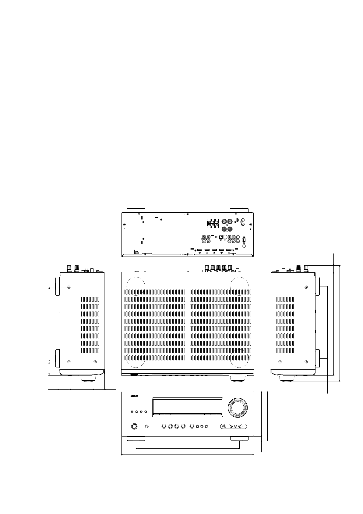
DIMENSION
50 dB Quieting Sensitivity :
[FM]MONO 2.8 μV (20.2 dBf)
S/N (IHF-A) :
[FM]MONO 70 dB
STEREO 67 dB
Total harmonic Distortion (at 1 kHz) :
[FM]MONO 0.7 %
STEREO 1.0 %
General
n
Power supply (for E3) : AC 120 V, 60 Hz
(for E2, EA) : AC 230 V, 50 Hz / 60Hz
(for E1C) : AC 220 V, 50 Hz
Power consumption :
330 W
0.5 W (Standby)
Maximum external dimensions :
435 (W) x 162 (H) x 382 (D) mm
Weight : 9.2 kg
Remote Control Unit (RC-1158)
n
Batteries : R03/AAA Type (two batteries)
Maximum external dimensions : 50 (W) x 211 (H) x 22 (D) mm
Weight : 110 g (including batteries)
245.0
43.5
30.5
86.0
30.5
162.0
236.8
54.7
21.5
22.0
338.5
382.0
340.0
435.0
15.0 147.0
5
Page 6
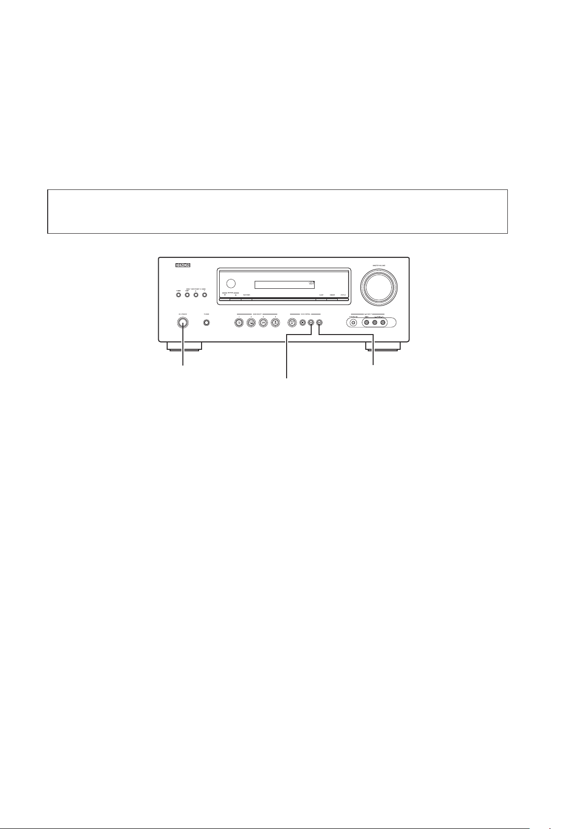
CAUTIONS IN SERVICING
Initializing AV SURROUND RECEIVER
AV SURROUND RECEIVER initialization should be performed when the μcom, peripheral parts of μcom, and Digital
P.W.B. were replaced.
1. Turn off the power pressing ON/STANDBY button.
2. Press ON/STANDBY button while simultaneously while pressing DOCK CONTROL
buttons.
3. Check that the entire display is ashing at intervals of about 1 second, and then release the 2 buttons.
The microprocessor will be initialized.
Note: • If step 3 fails, start over from step 1.
• All user settings will be lost and the factory setting will be recovered after the set is initialized.
So make sure to note down your setting beforehand for restoring after the initialization.
and DOCK CONTROL
8
9
ON/STANDBY
DOCK CONTROL 9
DOCK CONTROL 8
Service Jig
When you update the rmware, you can use the following
JIG (RS232C to internal connector conversion adapter).
Please order it from Denon Ofcial Service Distributor in your region if necessary.
8U-210100S :
606050028012P : 7P FFC(1.0) L-240 : 1 Set
(Refer to "PROCEDURE FOR UPGRADING THE VERSION OF THE FIRMWARE".)
WRITING KIT : 1 Set
6
Page 7
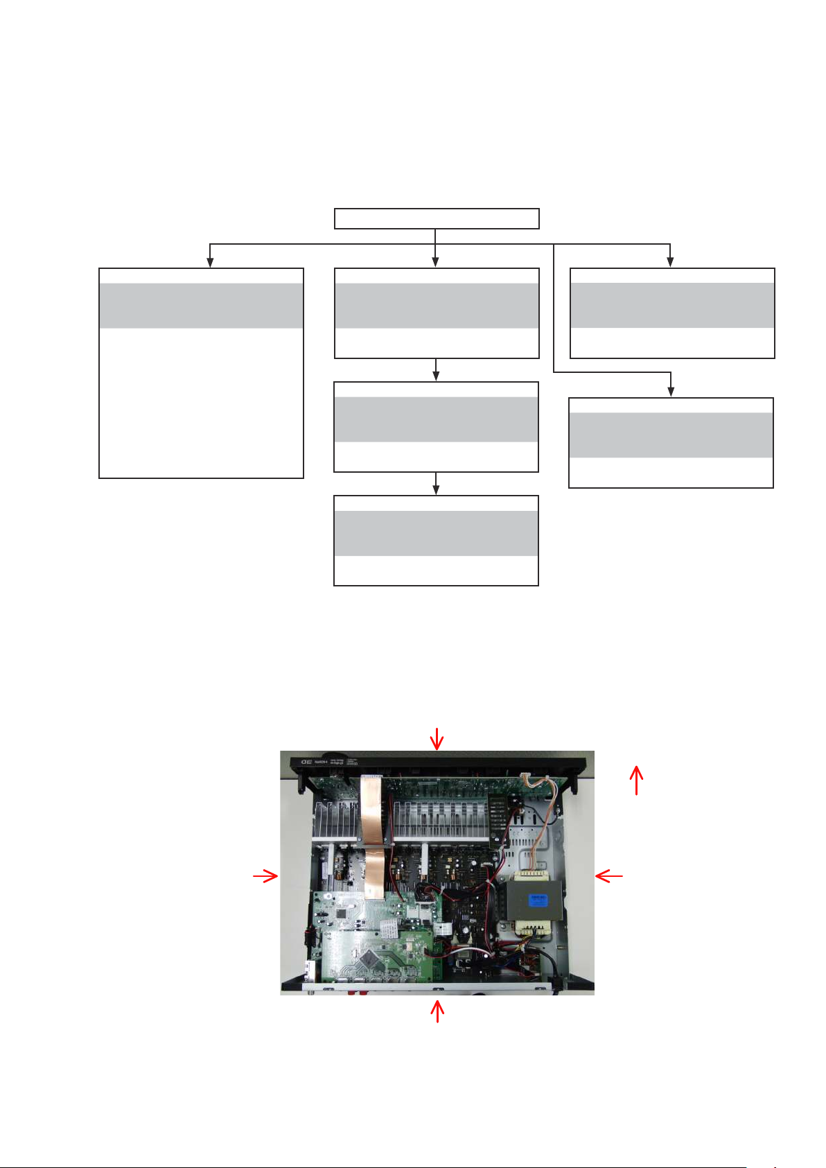
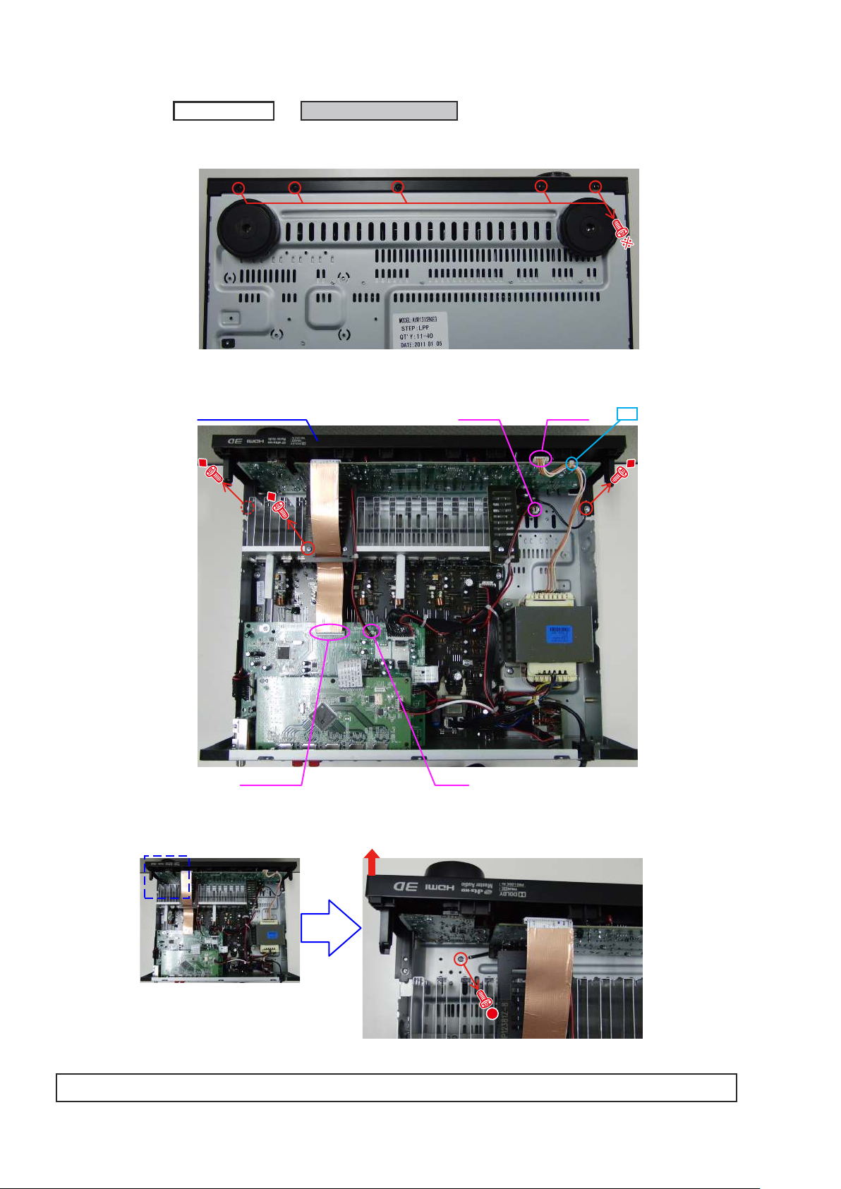
DISASSEMBLY
• Disassemble in order of the arrow in the following gure.
• In the case of the re-assembling, assemble it in order of the reverse of the following ow.
• In the case of the re-assembling, observe "attention of assembling".
• If wire bundles are untied or moved to perform adjustment or replace parts etc., be sure to rearrange them neatly as
they were originally bundled or placed afterward.
Otherwise, incorrect arrangement can be a cause of noise generation.
TOP COVER
FRONT PANEL ASSY
Refer to "DISASSEMBLY
1. FRONT PANEL ASSY"
and "EXPLODED VIEW"
PORTABLE IN UNIT
(Ref. No. of EXPLODED VIEW : C1)
VOLUME UNIT
(Ref. No. of EXPLODED VIEW : C2)
FRONT UNIT
(Ref. No. of EXPLODED VIEW : C3)
HEADPHONE UNIT
(Ref. No. of EXPLODED VIEW : C4)
POWER UNIT
(Ref. No. of EXPLODED VIEW : C5)
HDMI UNIT
Refer to "DISASSEMBLY
2. HDMI UNIT"
and "EXPLODED VIEW"
HDMI UNIT
(Ref. No. of EXPLODED VIEW : C11)
INPUT UNIT
Refer to "DISASSEMBLY
3. INPUT UNIT"
and "EXPLODED VIEW"
INPUT UNIT
(Ref. No. of EXPLODED VIEW : C10)
RADIATOR ASSY
Refer to "DISASSEMBLY
4. RADIATOR ASSY"
and "EXPLODED VIEW"
MAIN UNIT
(Ref. No. of EXPLODED VIEW : C6)
REGULATOT UNIT
(Ref. No. of EXPLODED VIEW : C7)
POWER TRANS
(Ref. No. of EXPLODED VIEW : C14)
POWER UNIT
Refer to "DISASSEMBLY
5. POWER UNIT"
and "EXPLODED VIEW"
POWER TRANS
Refer to "DISASSEMBLY
6. POWER TRANS "
and "EXPLODED VIEW"
About the photos used for "descriptions of the DISASSEMBLY" section
• The shooting direction of each photograph used herein is indicated on the left side of the respective photograph as
"Shooting direction: ***".
• Refer to the diagram below about the shooting direction of each photograph.
• Photographs with no shooting direction indicated were taken from the top of the set.
The viewpoint of each photograph
(Shooting direction)
View from the top
Shooting direction : B
Front side
Shooting direction: C
Shooting direction: D
Shooting direction: A
7
Page 8
1. FRONT PANEL ASSY
Proceeding :
(1) Remove the screws.
View from the bottom
(2) Cut the wire clamp band, then disconnect the connector wires and FFC cable. Remove the screws.
TOP COVER
FRONT PANEL ASSY
FRONT PANEL ASSY
CN603
CN610
cut
CN71FFC cable
(3) Remove the screws.
Please refer to "EXPLODED VIEW" for the disassembly method of each P.W.B included in FRONT PANEL ASSY.
8
Page 9
2. HDMI UNIT
Proceeding :
(1) Remove the screws.
Shooting direction: A
(2) Disconnect the connector wire and FFC cable.
TOP COVER
HDMI UNIT
HDMI UNIT
CN12FFC cable
9
Page 10
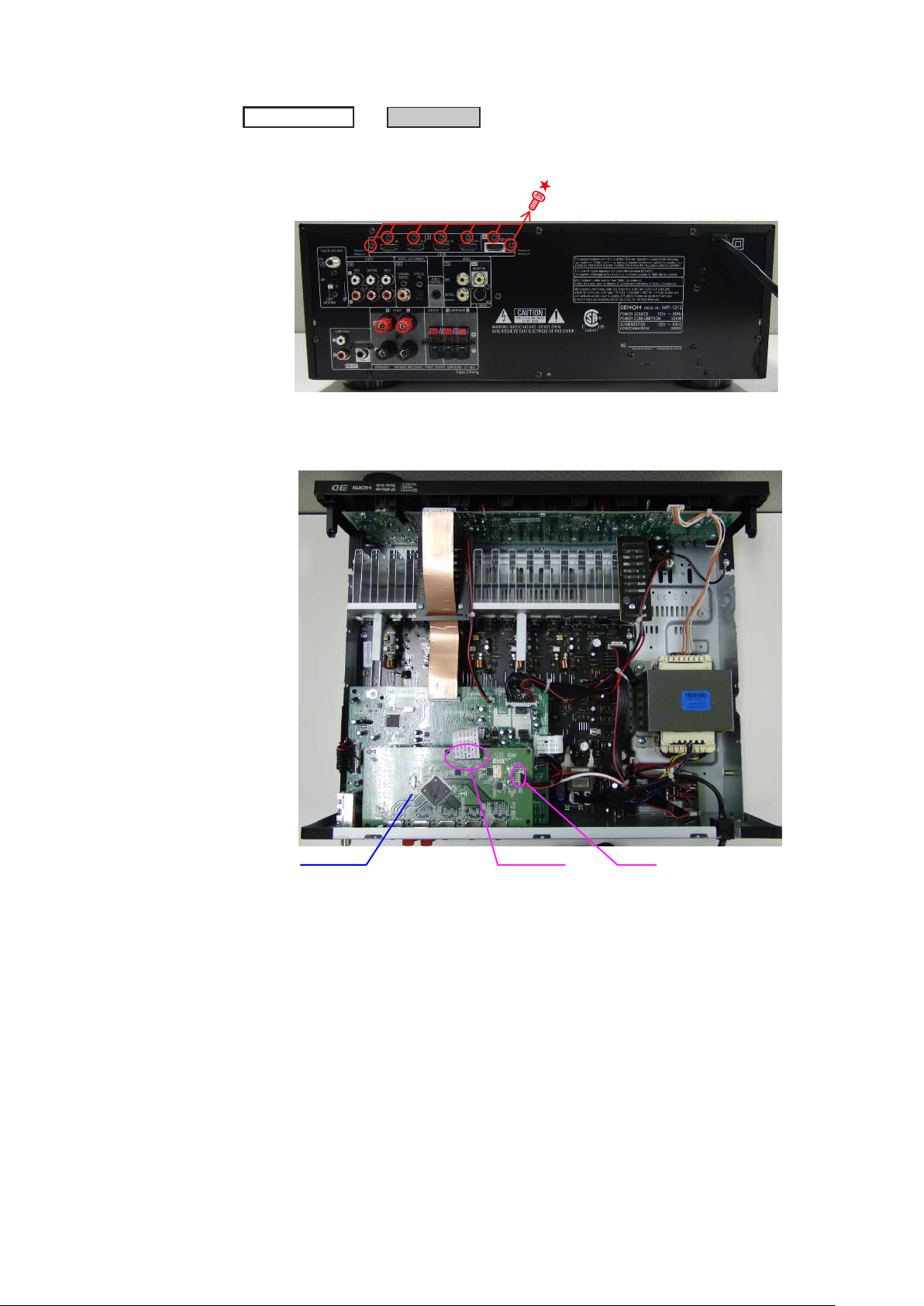
3. INPUT UNIT
Proceeding :
(1) Remove the screws.
Shooting direction: A
(2) Disconnect the connector wires and FFC cables, then remove the screws.
TOP COVER
HDMI UNIT
INPUT UNIT
FFC cable
CN71
cut
CN42
INPUT UNIT
FFC cableCN43
10
Page 11
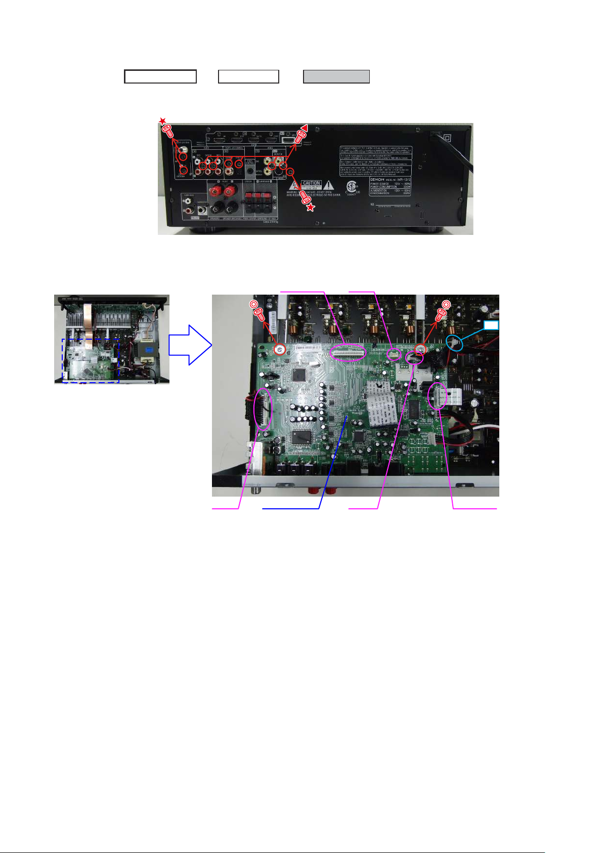
4. RADIATOR ASSY
Proceeding :
(1) Remove the screws.
Shooting direction: A
(2) Disconnect the connector wires, then remove the screws.
TOP COVER
HDMI UNIT
INPUT UNIT
RADIATOR ASSY
CN46
cut
CN45
cut
RADIATOR ASSY
(3) Disconnect the connector wire, then remove the screws. Remove the RADIATOR ASSY from the main unit.
CN47 CN48
CN41
Shooting direction: C
RADIATOR ASSY
Please refer to "EXPLODED VIEW" for the disassembly method of each P.W.B included in RADIATOR ASSY.
11
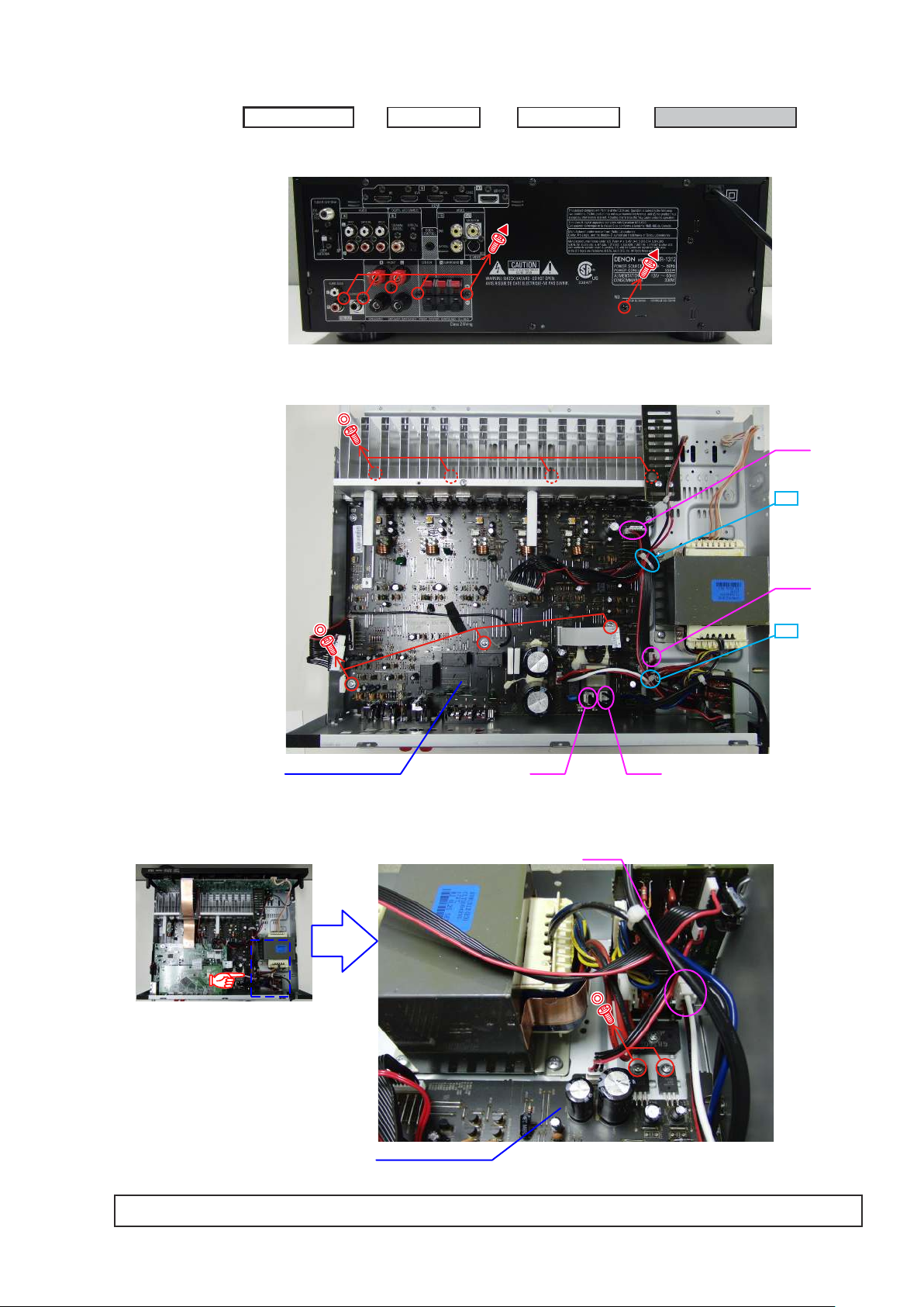
Page 12

5. POWER UNIT
Proceeding :
Please refer to "EXPLODED VIEW" for the disassembly method of POWER UNIT.
TOP COVER
POWER UNIT
6. POWER TRANS
Proceeding :
Please refer to "EXPLODED VIEW" for the disassembly method of POWER TRANS.
CABINET TOP
TRANS MAIN
12
Page 13
SPECIAL MODE
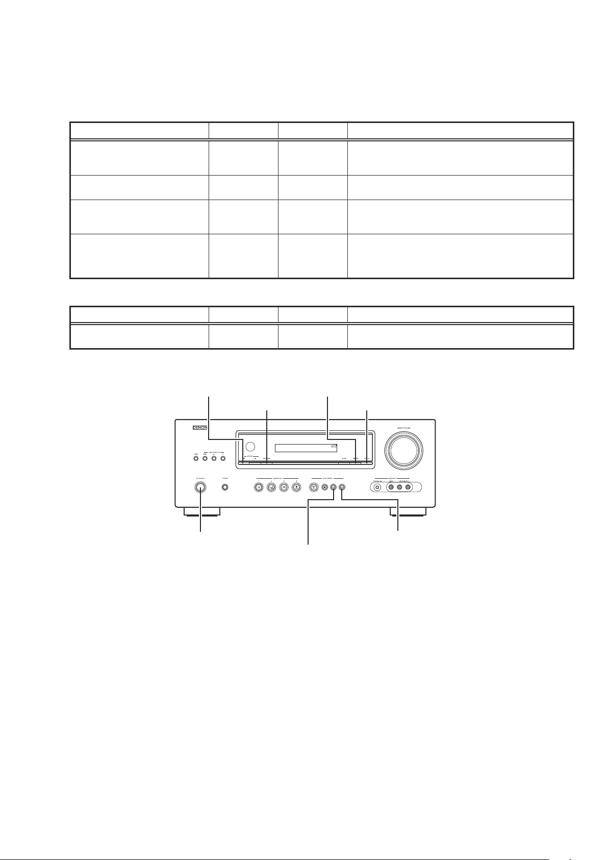
Special mode setting button
Press the ON/STANDBY button to turn on the power while pressing both the button A and the button B at the same
b
time.
Mode Button A Button B Contents
Firmware versions such as Main or DSP are displayed in the
µcom/DSP Version display mode STATUS DIMMER
Initialization mode
Mode for switching tuner frequency
step
Mode for preventing remote control
acceptance
When power is turned on, pressing both buttons A and B at the same time for 3 seconds or more.
b
Mode Button A Button B Contents
Select the video signal format STATUS DIMMER
DOCK
CONTROL
RESTORER SOURCE
8
DIMMER PRESET CH +
DOCK
CONTROL
FL display. Errors are displayed or when they occur.
(Refer to page 14 .)
Backup data initialization is carried out. (Refer to page 6 .)
9
---E2 model only---
Change tuner frequency step to AM9k/FM50kHz STEP or
AM:10k/FM:200kHz.
Operations using the remote control are rejected.
"REMOTE LOCK:ON" is displayed in FL display.
f
(Mode the cancellation: Turn off the power and execute the
same button operations as when performing setup.)
Select with the "+", "-" and iPod play button change video
format NTSC or PAL
ON/STANDBY
DIMMERSOURCE f
RESTORER
DOCK CONTROL 8
STATUS
DOCK CONTROL 9
13
Page 14
1. µcom/DSP Version display mode
1.1. Operationspecications
µcom/DSP version display mode:
When the set is started up in this mode, the version information is displayed.
Starting up:
Press the "ON/STANDBY" button to turn on the power while pressing the "RETURN" and "STATUS" buttons.
Now, press the "STATUS" button to the display the 2nd item information on the FL Display.
1.2. Display Order
Model destination information → w Main-µcom version → e DSP version → r OSD version
q
→ t iPod Dock version (Connecting iPod Dock)
Display State
Model destination information
q
AVR-1312 E3 model
A V R 1 3 1 2 E 3
AVR-1312 E2 model
AVR-1312 E1C model
Main-µcom version
w
DSP version
e
OSD version
r
iPod Dock version (Connecting iPod Dock)
t
(ASD-1R/11R)
(ASD-3/51)
A V R 1 3 1 2 E 2
A V R 1 3 1 2 E 1 C
M a i n : * * . * *
D S P . * . * . *
O S D : * * . * *
D o c k V e r : * * . * *
D o c k : I * * * * * * * *
Cleared of mode:
Press the "ON/STANDBY" button to turn the power off.
1.3. Error display
See the following table for each "Error information" display and its contents (status).
Condition - State
DSP NG When DSP boot, executing DSP reset makes to becomes error.
DSP OK (No error display, version display only)
D S P E R R O R 0 1
14
Page 15
WHEN THE MICROPROCESSOR IS REPLACED WITH A NEW ONE
When the U-PRO (Microprocessor) or the Flash ROM is replaced, conrm the following.
PWB Name Ref. No. Description
INPUT IC91 T5CN5 B SOFTWARE: Main
INPUT IC82 ST25VF080B-50-4C-S2AF B SOFTWARE: DSP ROM
After
replaced
Remark
After replacing
A
: Mask ROM (With software). No need for write-in of software to the microprocessor.
B : Flash ROM (With software). Usually, no need for write-in of software. But, when the software was updated, you should
write the new software on the microprocessor or ash ROM. Please check the software version.
C
: Empty Flash ROM (Without software). You should write the software on the microprocessor or ash ROM.
Refer to "Update procedure" or "writing procedure", when you write the software.
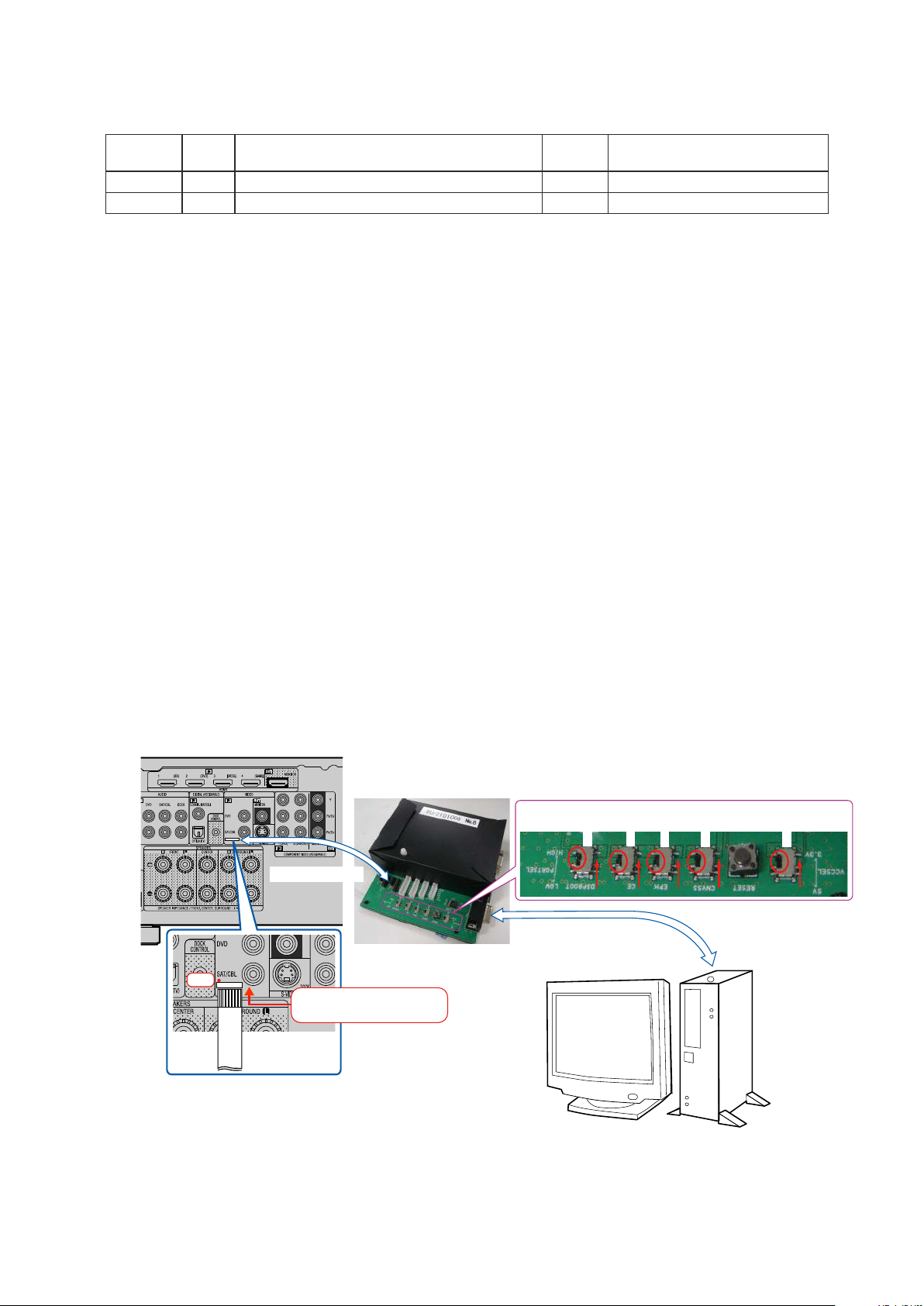
PROCEDURE FOR UPGRADING THE VERSION OF THE FIRMWARE
1. Preparations
1.1. Before starting the operation
(1) Personal Computer (Installed “BootTool_M330(Writing program).exe”).
(2) RS-232 cable (9P (Male), Straight).
(3) 8U-210100S Writing Kit.
(4) 606050028012P / 7P FFC(1.0) L=240.
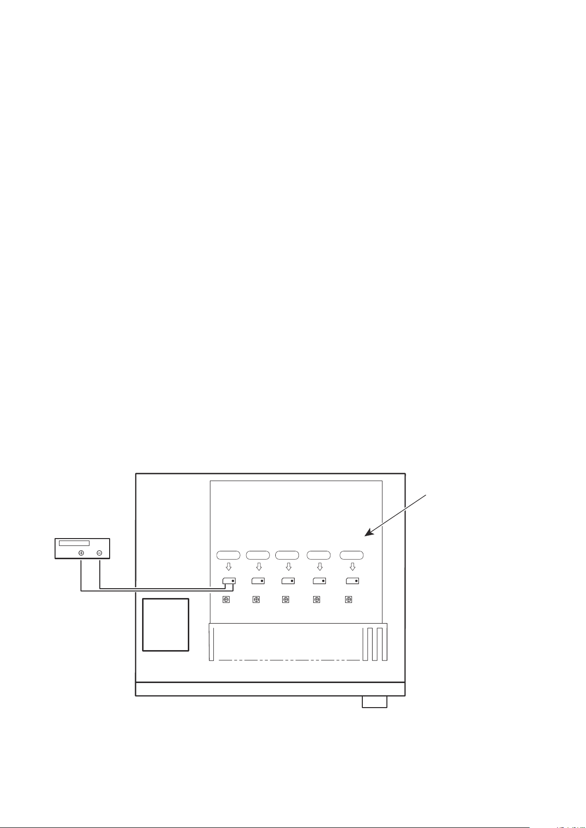
1.2. Connection of the AV receiver
(1) Conrm the power on/off switch of the AV receiver is turning off.
(2) Connect the update terminal of AV receiver with the “Writing Kit”.
(Refer to gure below for the connection of the 7P FFC cable.)
(3) Connect the RS-232C cable from PC with the “Writing Kit”.
7P FFC Cable
Writing Kit
1 pin
This side is contacts of
7P FFC Cable.
7P FFC Cable
S706-709 : HIGE
S709
S708
RS-232C Cable
S707
S706
S702 : 3.3V
S702
PC
15
Page 16
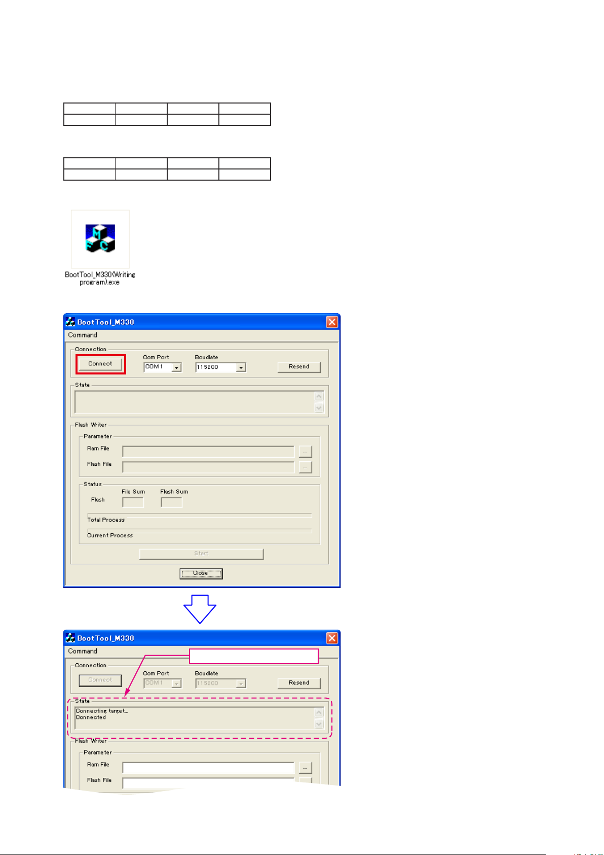
2. UPDATE FIRMWARE
(1) Connect the update terminal of AV receiver with the “Writing Kit”.
(2) Set the switch of “Writing Kit" (Refer to the table below).
DSPBOOT CE EPM CNVSS
H H H H
(3) Press the "ON/STANDBY" button to turn the power on of AV receiver.
(4) Set the switch of “Writing Kit" (Refer to the table below).
DSPBOOT CE EPM CNVSS
H H L H
(5) Press the "RESET" switch of “Writing Kit".
(6) Run the “BootTool_M330(Writing program).exe” on desktop of PC.
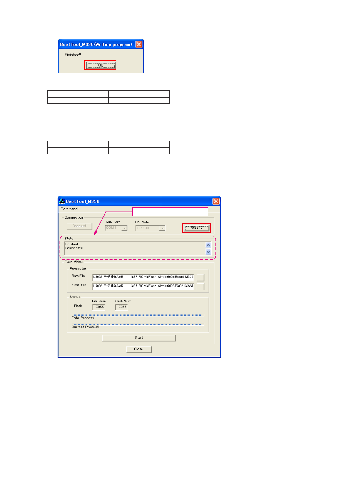
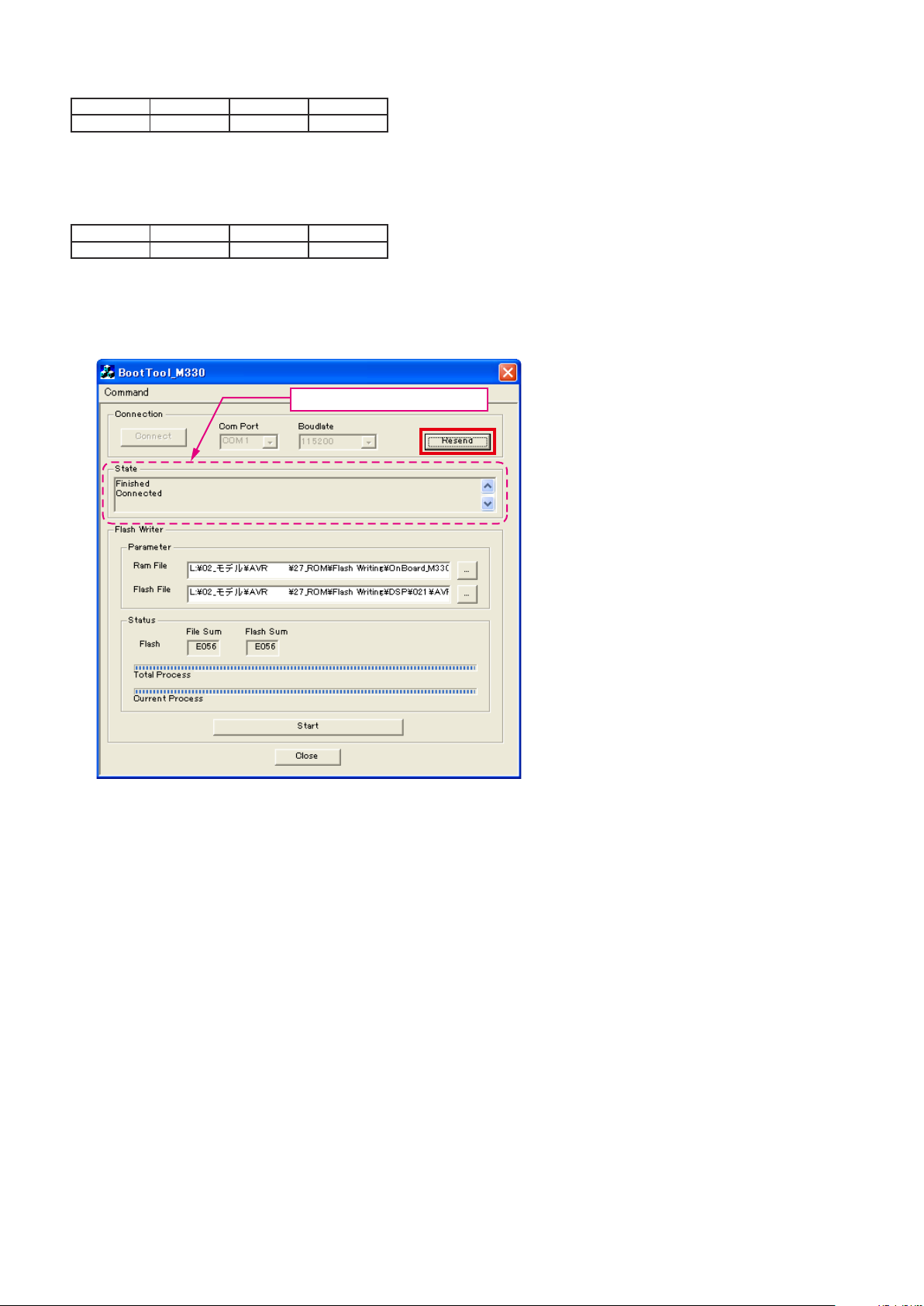
(7)-1 Click the “Connect” button.
"Connected" is displayed, it is OK.
16
Page 17
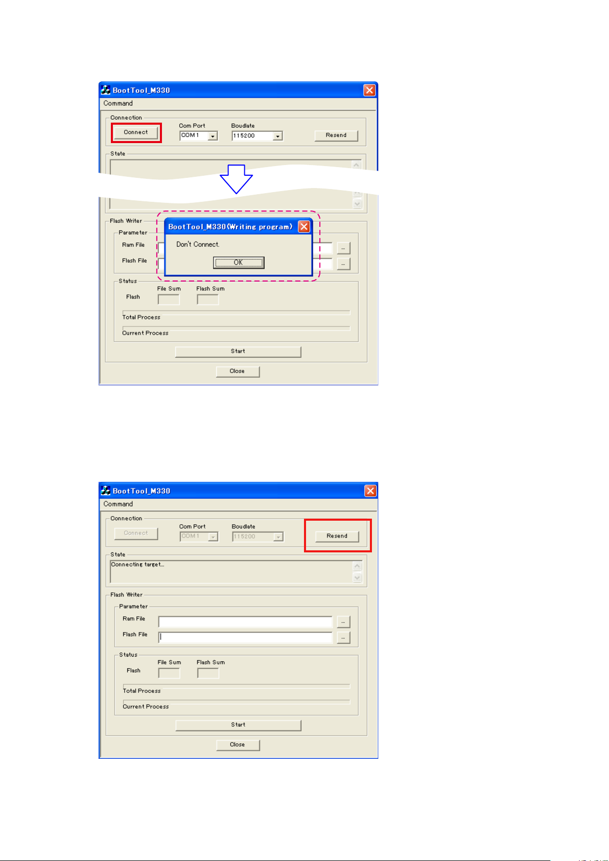
[ If you can't get a "Connected" message. ]
(7-a) Click the “Connect” button. If connection is not good, then you can see the “Don't Connect” message.
Please conrm the following
(i) Check the connection of the AV receiver and PC. (Refer to "1.2. Connection of the AV receiver" )
(ii) Check the selection of the RS-232C port number of PC.
(ii) Refer to "3. Notice: ". (page 27 )
(7-b) If Ram/Flash le selection screen is active, after you Click "Resend" button.
Connection is good, go to next step.
17
Page 18
SP SF1
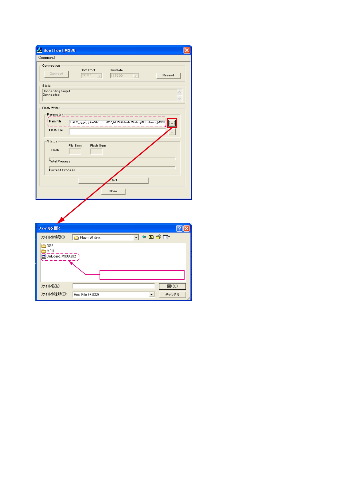
(8) Choose Ram File(OnBoard_M330.s32).
XXXX
Choose Ram File(OnBoard_M330.s32).
18
Page 19
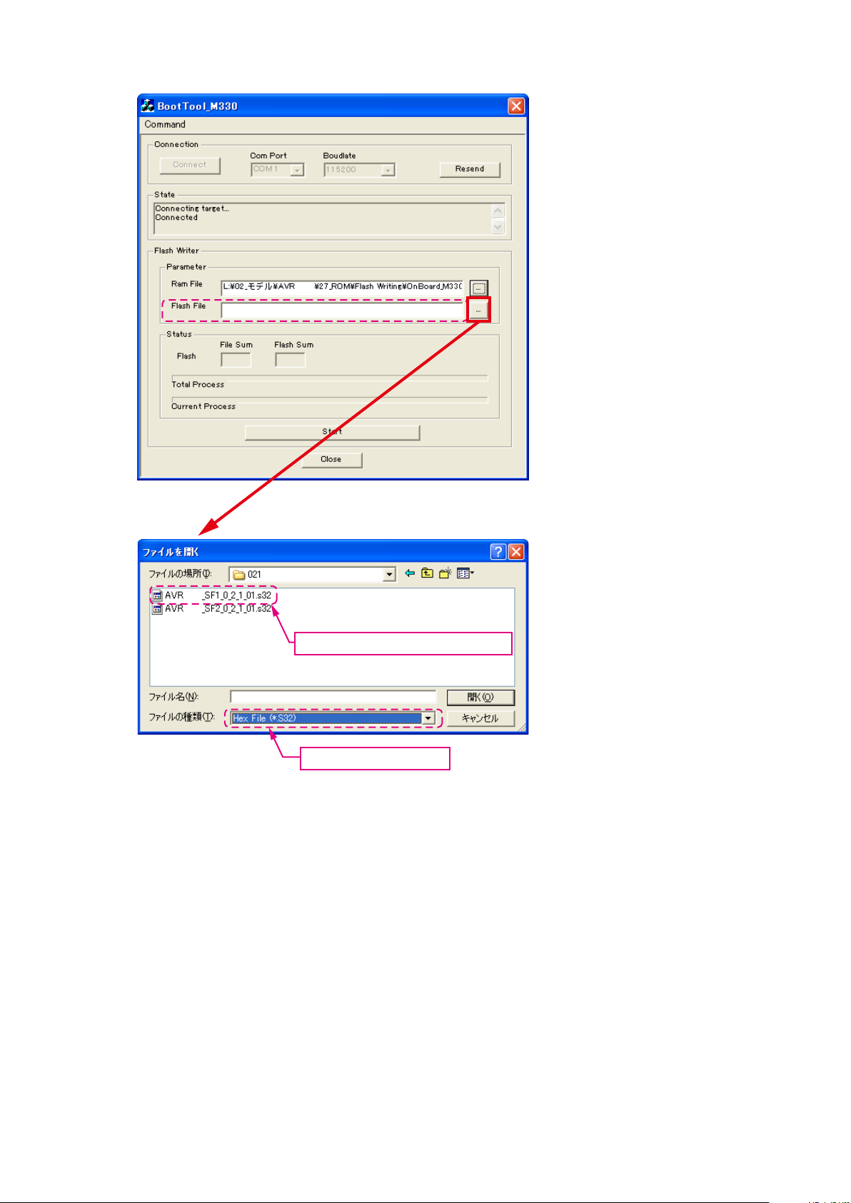
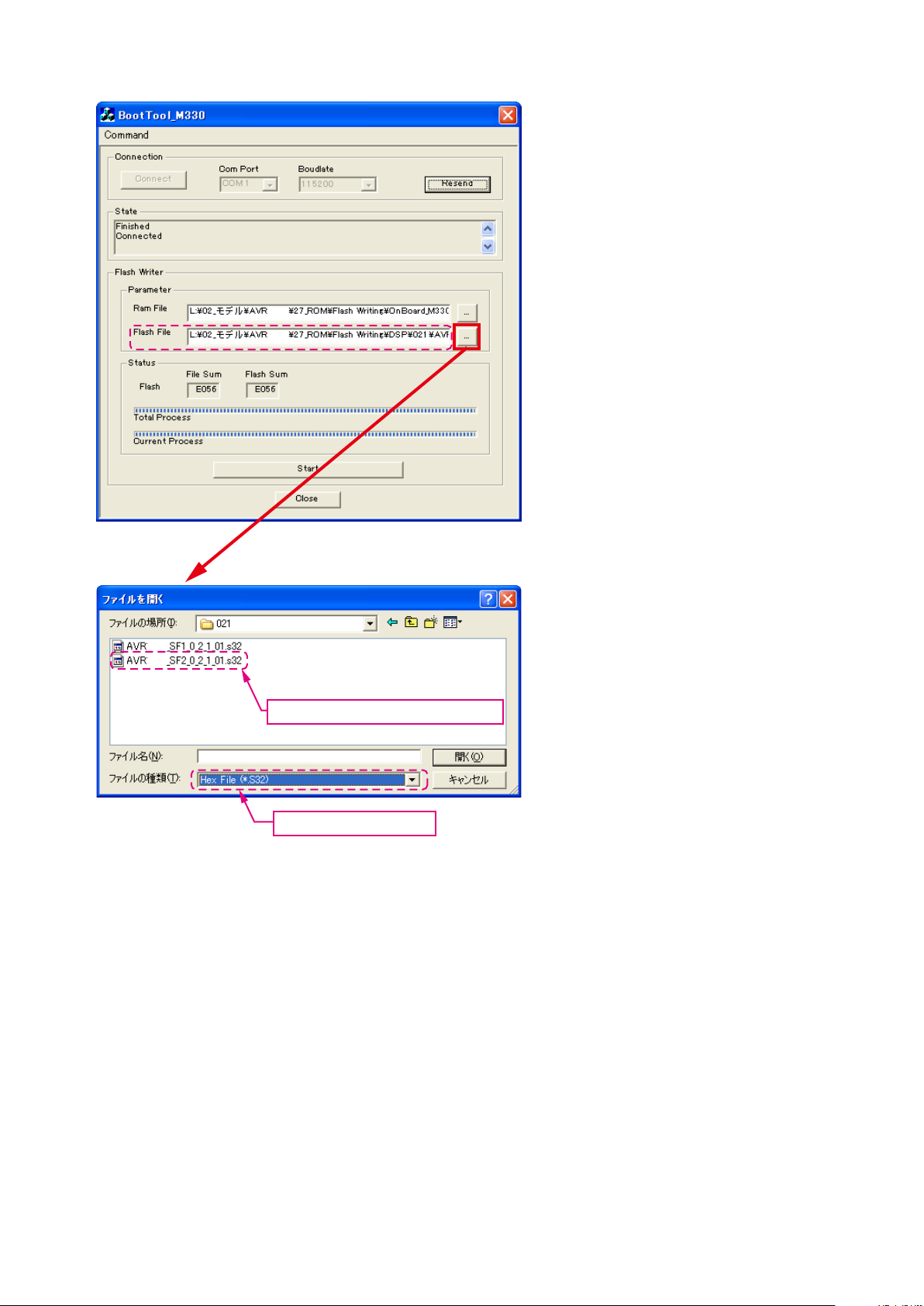
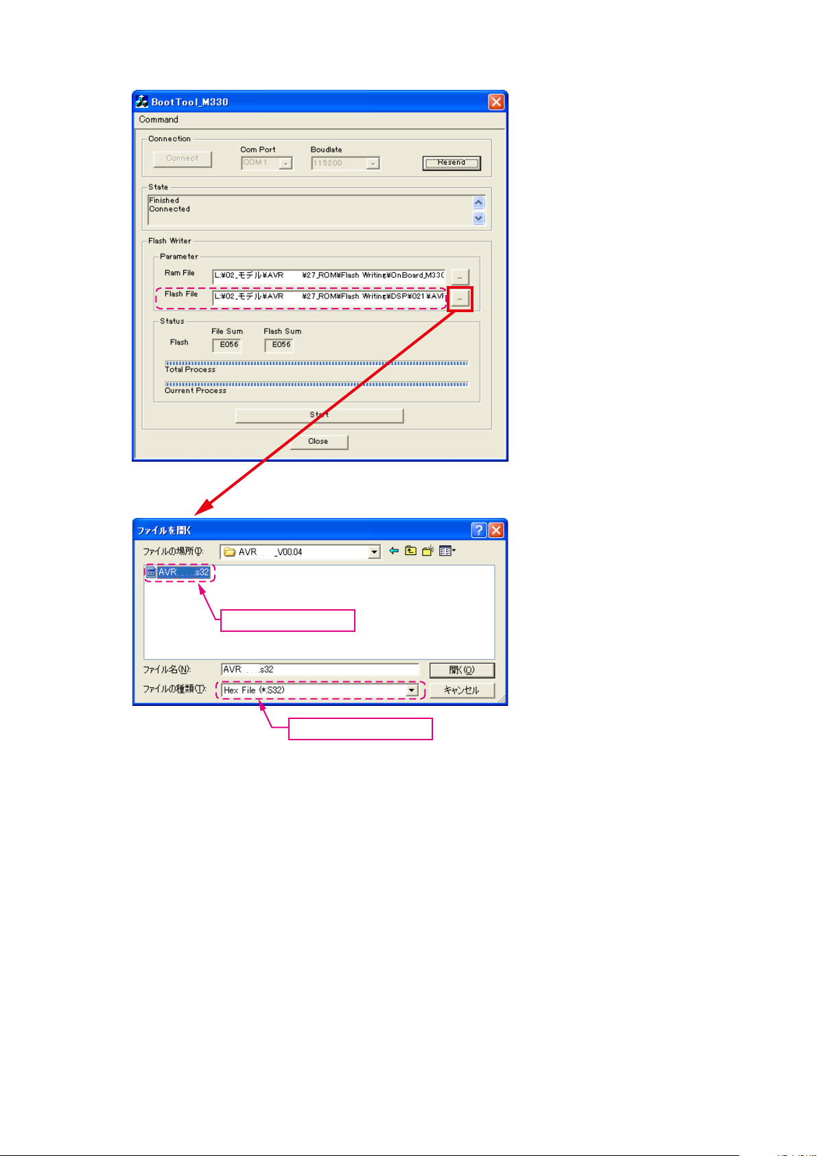
(9) Choose Flash File(DSP : SF1).
XXXX
XXXX
XXXX
Choose "AVRXXXX_SF1_*_*_*_01.s32".
Choose "Hex File (*.S32)".
19
Page 20
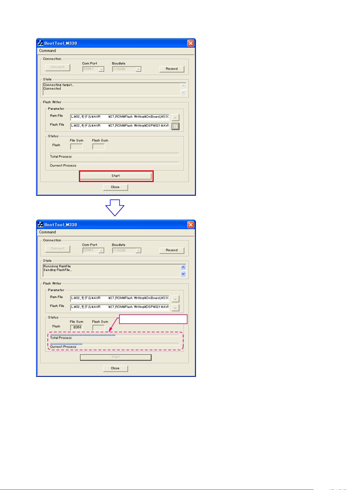
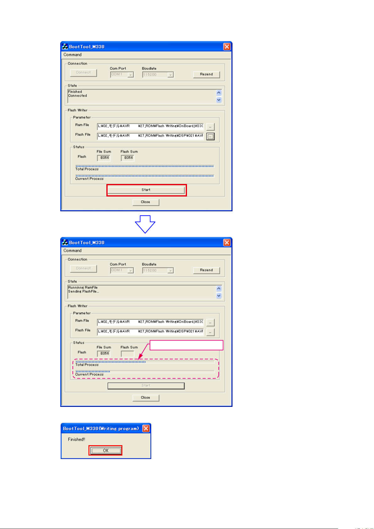
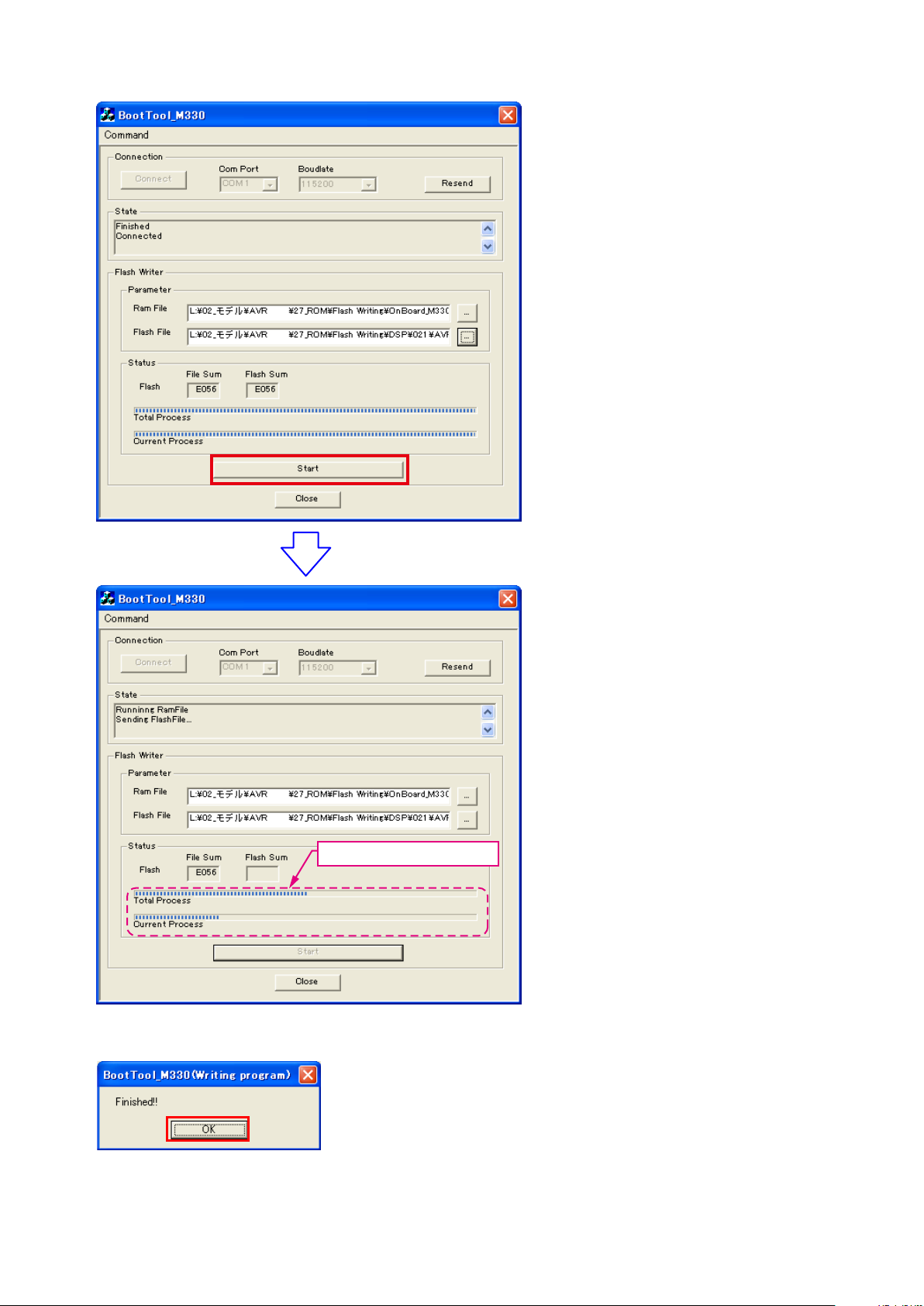
(10) Click the “Start” button.
XXXX
XXXX
XXXX
XXXX
The Setup Status bar appears.
20
Page 21
(11) "Finished!!" is displayed. Click the "OK"” button.
(12) Set the switch of “Writing Kit" (Refer to the table below).
DSPBOOT CE EPM CNVSS
H H H H
(13) Press the "RESET" switch of “Writing Kit".
(14) AV receiver is power on and starts update of DSP1.
(15) "Write Comleted" is displayed in the FL tube.
(16) Set the switch of “Writing Kit" (Refer to the table below).
DSPBOOT CE EPM CNVSS
H H L H
(17) Press the "RESET" switch of “Writing Kit".
DSP SF2
(18) Click the “Resend” button.
"Connected" is displayed, it is OK.
XXXX
XXXX
21
Page 22
(19) Choose Flash File(DSP : SF2).
XXXX
XXXX
XXXX
XXXX
Choose "AVRXXXX_SF2_*_*_*_01.s32".
Choose "Hex File (*.S32)".
22
Page 23
(20) Click the “Start” button.
XXXX
XXXX
XXXX
XXXX
The Setup Status bar appears.
(21) "Finished!!" is displayed. Click the "OK" button.
23
Page 24
(22) Set the switch of “Writing Kit" (Refer to the table below).
DSPBOOT CE EPM CNVSS
H H H H
(23) Press the "RESET" switch of “Writing Kit".
(24) AV receiver is power on and starts update of DSP2.
(25) "Write Comleted" is displayed in the FL tube.
(26) Set the switch of “Writing Kit" (Refer to the table below).
DSPBOOT CE EPM CNVSS
H H L H
(27) Press the "RESET" switch of “Writing Kit".
MAIN
(28) Click the “Resend” button.
"Connected" is displayed, it is OK.
XXXX
XXXX
24
Page 25
(29) Choose Flash File(MAIN).
XXXX
XXXX
XXXX
XXXX
Choose "AVRXXXX.s32".
XXXX
Choose "Hex File (*.S32)".
25
Page 26
(30) Click the “Start” button.
XXXX
XXXX
XXXX
XXXX
The Setup Status bar appears.
(31) "Finished!!" is displayed. Click the "OK" button.
26
Page 27

(32) Set the switch of “Writing Kit" (Refer to the table below).
DSPBOOT CE EPM CNVSS
H H H H
(33) Press the "RESET" switch of “Writing Kit".
(34) Initializing.
1. Turn off the power using ON/STANDBY button.
2. Press ON/STANDBY button while simultaneously pressing DOCK CONTROL
buttons.
3. Check that the entire display is ashing with an interval of about 1 second, and release your ngers from the 2
buttons and the microprocessor will be initialized.
Note: • If step 3 does not work, start over from step 1.
• All user settings will be lost and this factory setting will be recovered when this initialization mode.
So make sure to memorize your setting for restoring after the initialization.
and DOCK CONTROL
8
3. Notice:
Please keep the following notice for rmware update.
(a) Keep the PC environment
(b) Avoid the communication cable from the electrical noise source.
(e.g. telephone cable, AC line, a uorescent light)
(c) Don’t remove cable during update.
(d) Don’t turn off the power during update.
(e) Don’t run other PC application during update.
(f) Stop the resident program on PC (Virus checker and System check utilitu, etc)
(g) Stop the screen saver on PC.
(h) Stop the power save ability on PC.
(i) In case of laptop PC, Use the AC adaptor.
9
Conrmingthermware’snumberafterupgraded
After completion of the updating operation, the new version number can conrmed by starting up the AVR-1312 according
to the following procedure.
With the following operation, the AVR-1312 can be set to the Flash ROM Version-Number Conrmation mode.
Turn on power switch while simultaneously pressing "DIMMER" and "STATUS" buttons on the front panel. Every time the
"STATUS" button is pressed, version number of the Model, Main, DSP, … are indicated on the front panel section. (Refer
to "1.2. Display other" (page 14 ))
27
Page 28
ADJUSTMENT
Audio Section
Adjusting Idling Current
Required measurement equipment: DC Voltmeter
1. Preparation
(1) Avoid direct blow from an air conditioner or an electric fan and humidity should be moderate, and place the set at
normal usage environment.
Temperature should be at 15 °C ~ 30 °C.
(2) Presetting
• POWER (Power source switch) OFF
• SPEAKER (Speaker terminal) No load
(Do not connect speaker, dummy resistor, etc.)
2. Adjustment
(1) Removed the top cover and set VR41(FL),VR45(FR),VR42(C),VR44(SL),VR43(SR), on Main Amp. Unit at fully
counterclockwise position.
(2) Connect DC Voltmeter to test points (Front-Lch:CN51,Front-Rch:CN55,CENTERch:CN53,
Surround-Lch:CN52,Surround-Rch:CN54).
(3) Connect the power cord to AC Line, and set the power switch to "ON".
(4) Presetting.
MASTER VOLUME : "---" counterclockwise (
SPEAKER (Speaker terminal) : No load
(Do not connect speaker, dummy resistor, etc.)
FUNCTION : DVD
(5) Within 2 minutes after the power on, turn VR41 clockwise (
1.5 mV ± 0.5 mV DC.
(6) After 10 minutes from the preset above, turn VR41 to set the voltage to 2.0 mV ± 0.5 mV DC.
(7) Adjust the Variable Resisters of each channel (VR42-VR45) in the same way.
min.)
c
) to adjust the TEST POINT voltage at
x
DC Voltmeter
S Lch
F Lch
CN51
VR41 VR44 VR42 VR43 VR45
CN52
C ch
CN53
S Rch
CN54
F Rch
CN55
MAIN UNIT ASS'Y
28
Page 29
SURROUND MODES AND PARAMETERS
“Speaker Config.”.
S S
D. Comp z3 DRC z4 LFE z5
z2
Channel output Audio Adjust
S S
D S S S
z1
z2
“Bass Setting”), sound is output from the subwoofer.
S D
S D D D D S S
S D D D D S S
S D D D D S S
S D D D D S S
S D D D D S S
S D D D D S
S D D D D S S
S D D D D S S S
DOLBY PRO LOGIC g S D D D S S S
S D D D D S S
DTS NEO:6
DOLBY DIGITAL
DTS 96/24
DTS SURROUND
DOLBY TrueHD
DOLBY DIGITAL Plus
DTS Express
DTS-HD
z1 A signal for each channel contained in an input signal is output as audio.
z2 Only when “SW Mode” is set to “LFE+Main” (
z3 This item can be selected when a Dolby Digital or DTS signal is played.
z4 This item can be selected when a Dolby TrueHD signal is played.
z5 This item can be selected when a Dolby Digital or DTS signal or DVD-Audio is played.
VIRTUAL
MULTI CH STEREO
S D S S S
S D
Front L/R Center Surround L/R Surround Back L/R Subwoofer Mode
Surround mode)
Symbols in the table
S This indicates the audio output channels or surround parameters that can be set.
D This indicates the audio output channels. The output channels depend on the settings of
DIRECT (2channel)
S D D D D S
S D D D
DOLBY PRO LOGIC gx S D D D D S S S
STEREO
MULTI CH IN
DIRECT (Multi-channel)
29
Page 30
RESTORER z7
Tone
NEO:6 Music mode only
PRO LOGIC g/gx Music mode only
Panorama Dimension Center Width Center Image
Audio Adjust
S S
S S
z2
S
SB CH OUT Subwoofer
AFDM z6
Surround mode
DIRECT (2 channel)
S S S
DIRECT (Multi-channel)
STEREO
MULTI CH IN
DOLBY PRO LOGIC gx S S S S S S
DOLBY PRO LOGIC g S S S S S S
S S S S
S S S
DOLBY DIGITAL
DTS NEO:6
S S S
S S
S S S
S S S
DOLBY DIGITAL Plus
DOLBY TrueHD
DTS SURROUND
DTS 96/24
S S
S S S
DTS-HD
DTS Express
S S S
z2 Only when “SW Mode” is set to “LFE+Main” (“Bass Setting”), sound is output from the subwoofer.
z6 This item can be selected when a Dolby Digital or DTS or DVD-Audio signal is played.
z7 This item can be set when the input signal is analog, PCM 48 kHz or 44.1 kHz.
MULTI CH STEREO
VIRTUAL
30
Page 31

DOLBY
DIGITAL
DOLBY
DIGITAL
DOLBY
DIGITAL
DOLBY
DIGITAL EX
(2ch)
(4/3ch)
(5.1/5/4ch)
Flag)
(With no
DOLBY
(With Flag)
DIGITAL EX
DOLBY
DIGITAL Plus
DOLBY
TrueHD
DTS 96/24
DTS
(5.1ch)
Input signal types and formats
MTRX
DTS ES
DSCRT
DTS ES
DTS
High
DTS-HD
(With Flag)
(With Flag)
EXPRESS
Audio
Resolution
S F F F
F
F
S S F
F
F
F
Audio
Master
DTS-HD
(2ch)
LINEAR PCM
PCM DTS-HD DTS DOLBY DOLBY DIGITAL
(multi ch)
LINEAR PCM
S S S
z S S S
DTS EXPRESS
DTS + NEO:6
DTS NEO:6 CINEMA
S S S
DOLBY TrueHD
DTS NEO:6 MUSIC
DOLBY SURROUND
ANALOG
z F D
z F D
Surround mode NOTE
DTS-HD MSTR
DTS-HD HI RES
DTS ES DSCRT6.1
DTS ES MTRX6.1
Symbols in the table
F This indicates the default surround mode.
D This indicates the surround mode that is fixed when “AFDM” is set to “ON”.
S This indicates the selectable surround mode.
DTS SURROUND
DTS + PLgx MUSIC z S S S S
DTS SURROUND
DTS 96/24FDTS + PLgx CINEMA z S S S S
z S S S S
DOLBY DIGITAL+
DOLBY DIGITAL EX
DOLBY DIGITAL
DOLBY (D) +PLgx CINEMA z F D S S S
S S S
z If “Speaker Config.“ – “Surround Back“ (“Speaker Config.”) is set to “None”, this surround mode cannot be selected.
DOLBY PRO LOGIC g CINEMA S S S
DOLBY PRO LOGIC gx GAME z S S S
DOLBY PRO LOGIC gx MUSIC z S S S
DOLBY PRO LOGIC gx CINEMA z S S S
DOLBY (D) +PLgx MUSIC z S S S S
DOLBY PRO LOGIC g MUSIC S S S
DOLBY PRO LOGIC g GAME S S S
DOLBY PRO LOGIC
31
Page 32

DOLBY
DIGITAL
DOLBY
DIGITAL
DOLBY
DIGITAL
DOLBY
DIGITAL EX
DOLBY
DIGITAL EX
DOLBY
DOLBY
DTS 96/24
DTS
(2ch)
(4/3ch)
(5.1/5/4ch)
Flag)
(With no
(With Flag)
DIGITAL Plus
TrueHD
(5.1ch)
Input signal types and formats
MTRX
DTS ES
(With Flag)
DSCRT
DTS ES
(With Flag)
DTS
EXPRESS
High
DTS-HD
Resolution
Audio
Master
DTS-HD
(2ch)
LINEAR PCM
PCM DTS-HD DTS DOLBY DOLBY DIGITAL
(multi ch)
LINEAR PCM
ANALOG
Audio
F
F D (7.1)
F S F S S S S S S S S S S S S S S
S S S S S S S S S S S S
S S S S S S S S S S S S
S S S S S S S S S S S S S S S S S
z If “Speaker Config.“ – “Surround Back“ (“Speaker Config.) is set to “None”, this surround mode cannot be selected.
Surround mode NOTE
MULTI CH IN
MULTI CH IN + PLgx CINEMA z S
MULTI CH IN
MULTI CH IN 7.1
MULTI CH IN + PLgx MUSIC z S
DIRECT
MULTI CH STEREO
DIRECT
DSP SIMULATION
VIRTUAL
STEREO
STEREO
32
Page 33

TROUBLE SHOOTING
1. POWER
1.1. Power not turn on
Power not turn on.
Is the ON/STANDBY
indicator on the front panel
ashing red?
YES
Are there any incomplete
connections in the
connectors connecting
between the various circuit
boards?
Is there a short circuit
NO
between the speaker
terminals and the ground?
Correct the short
YES
circuit between the
speaker and ground.
NO
Is the fuse blown?
NO
Does the power turn on
when the POWER switch is
turned off then back on?
YES YES YES
Check the primary circuitry
parts including the POWER
switch(for poor contacts,
etc.), and replace any
defective parts.
YES
Connect the connectors
property.
YES
Refer to "1.2. Fuse is blown".
Is a DC 5V voltage being
NO NO
supplied from the MAIN B'd
to the microprocessors?
Check the microprocessor
periphery circuitry and
replace any defective parts.
NO
Check for damage in the
power amplier circuitry
parts and replace any
defective parts.
Is a DC5V voltage output
when the cord supplying the
power from the MAIN B'd to
the microprocessor(BN43)
is unplugged?
Check the circuitry and parts
from BN43 on the MAIN
B'd to the microprocessor
for damage and short-
circuits,and replace any
defective parts.
Check the parts from
NO
IC45 to the primary
circuitry and replace
any defective parts.
1.2. Fuse is blown
Check for leaks or short
circuits in the primary side
parts and replace any
defective parts.
Fuse is blown
Check for short circuits in the
rectier diodes and circuitry of
the secondary side rectifying
circuits and replace any
defective parts.
After repairing, also replace the fuse.
33
Check for short circuits in
the power stabilizer unit's
regulator output terminal and
the ground and replace any
defective parts.
Page 34

2. Analog video
MONITOR OUT(CVBS) Output NG
Check ±5V
+5V : C755
-5V : C754
YES
Check output
Output V : IC71-1pin
YES YES
Check cable between main unit and
monitor or Check monitor.
VIDEO test point
BK61
BK61
JK72
C772
R763
R764
JK73
C766
IC72
C765
C769
C768
C757
IC71
A
7
R766
R760
R76
C860
RN85
R823
R861
R852
C726
IC70
C961
6.+5VD
7.+5VD
8.DGND
9.DGND
5.DGND
10.-12V
C770
R765
C759
C756
C754
R768
SCLK
R771
R846
C843
IC81
RN86
R866
R851
R867
R853
R854
RN88 RN87
R855
RN89
RN90
IC69
CN8A
C749
C751
1.VGND
3.VGND
2.AUX_CV
IC
11.PRE_GND
15.MCUGND
13.+12V
12.PRE_GND
14.MCU+5V
C780
C779
C755
IC83
C859
C771
C718
7805
BD62
0
6
C9
1.VGND
3.+5VH
2.+5VH
4.DGND
1.PROTECTION
2.FRONT_RLY
3.C_SUR_RLY
4.C_SUR_RLY
5.HP_RLY
6.P_DOWN
7.SB_MUTE
8.SUB_MUTE
9.PWR_RLY
10.LIMIT_DET
11.LIMIT
12.NC
13.NC
C785
C789
C787
C783
C778
C781
C782
R782
R781
R783
R780
R779
R778
C797
C795
C793
C796
IC73
C799
BN12
C791
C792
RN83
R785
1.+5VH
R784
C790
2.+5VH
3.DGND
RN84
4.DGND
5.+1V8
C730
C731
BD63
C629
O
I
G
7905
IC74
R940
IC68
7805
J1
C720
C745 CN9 A
C747
IC60
CN43
ET71
C958
C957
C959
INPUT (COMPONENT SIDE)
C764
C763
R845
R847
R844
RN80
IC82
C728
R609
R613
C724
C725
CN71
MP_CUP12375Z
ICT
ADJ1
JK71
C811
RXP2
C824
C822
C826
C825
C827
C882
SDOUT
C806
R808
C804
R809
R812
R813
LRCK
CLK
LRCK
DATA0
R842
C839
X801
R839
R838
R837
R819
RN82
X-OUT
1
RN8
R860
R856
R859
C842
R857
R858
R881
R826
R827
R825
R824
D605
R736
R612
946
R
R945
C722
D606
R944
R942
R943
1.HDMIOSD_MI
C723
R737
ADJ2
RP
NO
The power supply circuitry is
defective.
Check input
NO NO
(When the DVD function)
Vin5 : IC71-3pin
Check pattern from JK71 to IC71 and
check cable between AMP and player or
check player .
Check set value of IC.
SW1 : IC71-14pin : 3.3V : OK
SW2 : IC71-10pin : 3.3V : OK
NO
CPU(IC91) aw.
SW3 : IC71-4pin : 3.3V : OK
SW4 : IC71-6pin : 3.3V : OK
YES
The IC71 and surrounding
circuitry is defective.
8
5
6
R659
CN91
R922
R923
R921
JK91
C816
BD83
C814
IC84
24.576MHz
IC85
C836
R828
5.DGND
3.HDMIOSD_CS
6.HDMIOSD_HOLD
2.HDMIOSD_MO
4.HDMIOSD_CLK
23.MCUGND
JK81
JK82
C830
C975
R935
C924
C923
757
C743
R
R758
C742
R936
IC67
C815
C737
C813
05
R8
C741
R754
C658
C660
R670
C656
R671
R676
R672
R677
R673
C657
C659
C810
C808
C676
C674
C672
R686
R687
R692
R688
R693
R689
C673
C675
C693
C691
C689
R702
R703
R708
R709
R704
R820
R705
C690
C692
J3
C707
C709
C705
R718
R724
R719
R720
829
R725
R830
R
R721
C706
3
2
R79
R79
R959
7.DGND
8.HDMI_SDA
12.INT1_RX
10.HDMI_SCL
16.DGND
9.DGND
21.HDMI_LRCLK
18.HDMI_SDAA1
13.INT2_RX
15.HDMI_RST
14.INT_TX
17.HDMI_SDAA0
19.HDMI_SDAA2
11.DGND
22.HDMI_SCLK
23.HDMI_MCLK
20.HDMI_SDAA3
D94
BD92
BD93
BD95
BD91
B
8.VOL-
11.KEY1
13.STBY _LEDG
10.KEY2
9.KEY3
18.VFD_DATA
21.MCU+3V3
12.STBY _LDER
15.VFD_RST
20.MCU+3V3
14.REMOTE_IN
19.PWR_RLY
17.VFD_CLK
16.VFD_CE
22.MCUGND
C974
C829
0
9
R791
R7
35
C7
R745
C736
R746
IC66
R748
R678
94
R7
C661
R679
IC62
C662
R681
R680
C665
R795
R694
R695
C678
R796
IC63
C679
R697
R797
R696
R710
98
R7
R711
C694
IC64
C695
C698
R713
R799 C682
R712
R726
7
0
2
R7
R80
C710
IC65
R652
C711
C708
9
R738
R72
R728
Pb
A30C5/C5
J2
CN1A
1.+12V
2.-12V
3.VAUX_L
5.VAUX_R
5.MCU+5V
6.3D_LEDB
7.N.C
7.VOL+
4.AGND
6.HP_DET
0
4
2
25
6
6
R615
R622
C619
R
C62
C627
R
R623
C628R624
R626
R621
C623
R619
R617
C617
C732
C618
C663
C664
IC61
C638
C640
C636
C680
C681
C641
C639
C637
C696
C650
C646
C717
C697
R735
C712
C713
Q608
Q609
33
32
9
9
R
R
R931
R930
R929
R920
IC91
RN91
C913
RN92
C916
C915
C914
R912
1
91
C
5
4
1
RN93
R91
X901
C917
R913
R9
10MHz
CN2A
1.-12V
2._MIC_DET
3.MIC_SIGNAL
4.AGND
1312E2/EA
R916
10K
R917
X
BARCODE LABEL
1312E1C
1312E3
10K
4K7
R
TU61
C611
C612
C610
C613
JK62
7
0
R6
R608
R638
6
C635
620
R618
R61
C
C634
R639
L602
R640
C633
R651
R643
R642
C643
C648
C644
C642
C645
IC94
CN93
CN92
R937
R956
R955
C908
C907
C906
02
3
R9
R90
C905
7
R928
R926
R92
C918
Q901
R917
R916
R901
IC92
10K
10K
INT
RESET
CE
SDIO
L601
SCLK
VCC
R-OUT
L-OUT
C607
CN42
ET01
1.FL
2.AGND
3.SL
4.AGND
5.CT
6.AGND
7.SR
8.AGND
9.FR
10.AGND
11.SW
C649
12.AGND
13.SBR
14.AGND
15.SBL
C921
C919
IC93
IC95
C902
C904
R905
R906
904
R
C909
IC96
C954
Q903
R954
R910
C926C927
ET91
Detail A
C955
03
9
D
R908
R953
C956
C928
C779
SW1 SW2
R765
34
C860
IC71
R766
R760
RN85
C755
+5V
Output V SW3Input V SW4
R767
C757
R771
R768
C756
C759
C754
-5V
SCLK
R846
R844
Page 35

3. HDMI/DVI
3.1. No picture or sound is output
No picture or sound is output.
Check HDMI/DVI cable connection.
(1) Is the HDMI/DVI cable properly connected?
YES
(2) Are you using an HDMI/DVI selector, repeater or a device for
improving picture quality?
NO
(3) Are you using a certied HDMI cable (with the HDMI stamp)?
YES
(3) Are you using an HDMI/DVI cable less than 5 meters in length?
YES
(4) Are the picture and sound output when another HDMI/DVI cable
is used?
NO
d
NO
There may be the a problem with the HDMI/
DVI cable. Check connection.
YES
Disconnect everything and connect only the
HDMI/DVI cable to check
NO
Use a certied HDMI cable (with the HDMI
stamp).
Replace the HDMI/DVI cable with one that
NO
is less than 5 meters in length (2 meters
recommended) to check.
YES
The HDMI/DVI cable is defective.
Check BD/DVD player.
(5) Is the BD/DVD player's HDMI output setting correct?
YES
(6) When you use a DENON BD/DVD player's, is the uorescent
display tube's "HDMI" indicator lit? If you use a non-DENON BD/
DVD player's, proceed to
NO
(8) Is sound output from the set's speaker terminals when the TV's
power is turned off or the connection cable between the TV and
the set is disconnected?
"YES".
YES
(7)
Are the picture and sound output
when the BD/DVD player's
resolution is changed?
NO
NO
(9) Are the picture and sound
output when a different BD/
DVD player is used?
NO
NO
Check the HDMI output setting, referring to
the BD/DVD player's operating instructions.
YES
Set the BD/DVD player output resolution to
a resolution with which the TV is compatible.
YES
The BD/DVD player may not be compatible
with HDCP repeaters. Ask the BD/DVD
player's manufacturer.
YES
The BD/DVD player is defective.
35
Page 36

Check TV
(10) Is the TV HDCP-compatible?
YES
(11) Is the TV compatible with resolutions of 1080P?
YES
(12) Is the TV's input set to HDMI?
YES
(13) Are the picture and sound output when a different TV is used?
YES
Check set (AVR-1312)
Is a contact part of HDMI connector normal? (Refer to 37 page (*1).)
YES
NO
Use an HDCP-compatible TV. PC TVs
cannot be used.
If the TV is not compatible with resolutions
NO
of 1080P, no picture will be output, even
if the BD/DVD player's resolution is set to
1080P.
NO
Check the TV's input setting, referring to the
TV's operating instructions.
NO
The TV is defective.
NO
The HDMI connector is defective.
Replace the new HDMI connector.
(14) Is the set's input set to HDMI?
YES
The set does not recognize the TV.
(15) Is test point (HPD_O) set to the "H"(3V-5V)?
With the TV connected, Check voltage of the IC on the side on
which the TV is connected.
Is communication waveform conrmed in Test point (DDC_CLK/
DDC_DATA)?
Is terminate the TMDS signal
D145/D146/D147/D148/D149/D150?
YES
(16)
When using a DENON
BD/DVD player, is the FL
display's "HDMI" indicator lit?
If using a non-DENON BD/
DVD player, proceed to "NO".
is
3.3V
conrmed in
The BD/DVD player does not recognize the
connection with the set.
(17)
Is HDMI connector Test point (HPD) set to the
"H"(3V-5V)?
NO NO
With the BD/DVD player connected, Check
voltage of the HDMI connector for the input on the
side on which the BD/DVD player is connected.
Is communication waveform conrmed in Test
point (DDC_CLK/DDC_DATA)?
Is terminate the TMDS signal
each HDMI connector?
HDMI IN1 : D133 : 140
HDMI IN2 : D123 : 130
HDMI IN3 : D113 : 120
HDMI IN4 : D103 : 110
D143/D144/
is
NO
Check the set's input setting, referring to the
set's operating instructions.
The pattern and circuit from the HDMI
NO
connector (JK15) to the IC11 is defective, or
HDMI output circuitry is defective (IC11 and
surrounding circuitry).
Replace the IC11.
The pattern and circuit
from the HDMI connector
(JK11/JK12/JK13/JK14)
to the IC11 are defective.
3.3V
conrmed
of
Replace the IC11.
YES
Check operation of IC11.
(Video input 480P from BD/DVD players / Connect the TV.)
Replace the IC11.
YES
36
Page 37

(18) Check power supply.
Are 1.8V or 3.3V supplied to IC11 (each power supply pin)?
YES
(19) Check xtal oscillator.
Is there 28.6363MHz oscillation of X101?
YES
NO
The power supply circuitry is defective.
NO
The X101 or IC11 is defective.
Replace the new parts.
(20) Check RESET.
Is RESET waveform conrmed at IC11 (97pin)? (If reference
waveform, proceed to "YES".)
YES
(21) Check control signal(I2C).
Is waveform conrmed at Test point (SDA/SCL). (If not continued
to " L", proceed to "YES".)
YES
HDMI output circuitry is defective (IC11 and surrounding circuitry).
Replace the IC11.
(*1) Abnormal sample of HDMI connector : The internal terminal has bent.
NO
The RESET pattern or IC11 is defective.
Replace the new parts.
NO
The SDATA/SCL line pattern is defective.
37
Page 38

3.2. HDMI test point and waveforms
C
R108
D
BK11
+5V_O
L114
JK15
C162
C161
A
L113
150
D149
D
IC13
D146
D145
48
1
D143
D144
D147
D
C153
C152
C157
C156
59
C158
C160
L301
1.+5V
R301
2.+5V
3.GND
C304
C303
C302
4.GND
5.+1V8H
L109
C165
C170
CN12
C168
T105
T104
(GND)
(+8V)
CN11
4.VCC
3.MISO
1.SCK
2.GND
6.MOSI
5./CS
C1
C155
C154
C179
8
16
R
IC16
301
C
4
C33
T103
(POK)
C174 C173
C169
L110
98
7.GND
R1
R200
R196
R199
JK11
D152
HPD_O
R183
D153
D110
DDC_CLK_O
R124
D109
R148
DDC_DATA_O
D107
D108
R147
C182
R180
145
R
R181
R146
R179
41
C181
1
D
D142
R170
R169
C178
(EAOUT)
T102
R167
(AGND)
T101
R103
C167
C185
C166
C164
IC15
C163
CN8B
MI
MO
CS CLK
D105
D106
D104
D103
R162
D
SCL
SDA
INT1
INT2
R109
C102
B
HPD_3
D115
A
A
R175
R176
DDC_CLK_3
A
+5V_3
R193
R107
3
1
D114
D1
R108
R192
IC11
B
A
B
C
A
R177
3.CS
2.MO
1.MI
R110
Q103
Q104
JK13
R186
D111 R111
D112 R172
30
D129
D1
28
D1
DDC_DATA_3
B
B
B
A
5
3
RN11
1
R
R136
R157
7
9
33
1
R
R134
R132
R1
4.CLK
6.HOLD
10.SCL
13.INT2
7.GNDB9.GND
5.GND
8.SDA
12.INT1
11.GND
R105
Q101
Q102
JK12
R187
HPD_4
+5V_4
119
D
D120
R104
C101
DDC_CLK_4
R195
R101
R102
R194
D101 R106
R164
C180
RESET
INT_TX
D0
D116
D118
D117
DDC_DATA_4
A
: 1.8V
B
: 3.3V
71
1
R
D102
B
C332
A
A
122
C137
R123
R
A
R178
IC14
MCLK
SCLK
LRCLK
D1
D2 D3
R114
C103
R115
Q105
JK14
HPD_2
D125
D126
D124
D127
A
A
B
B
A
R142
A
RN12
Q106
R185
73
1
+5V_2
R
R116
9
36
D13
D135
D1
D140
2
12
D121
D
B
137
R191
DDC_CLK_2
R112
DDC_DATA_2
R113
R190
C333
X101
C146
5
C14
C331
D138
D
28.636 36 MHz
BAR CODE LABEL
D123
A
R143
R144
R141
MP
CUP12376Z_A(MP)
IC ICT
18.SDATA1
17.SDATA0
14.INT_TX
21.LRCLK
15.RESET
16.GND
19.SDATA2
20.SDATA3
22.SCLK
23.MCLK
ADJ1
D134
D133
ADJ2
HPD_1
DDC_CLK_1
Pb
A30C5/C5
D131
121
R
RP
+5V_1
DDC_DATA_1
D132
R184
R174
R117
R188
BK12
R120
R118
R119
C104
Q107
Q108
189
R
DIPPING
Detail A
+5V
+5V_O
TMDS D2+
BK11
TMDS D0+
TMDS D2-
L114
C162
C161
L113
IC13
C160
D150
C152
JK15
D149
C153
D148
C154
TMDS D1+ TMDS CK+
TMDS D1- TMDS CK-
TMDS D0-
D146
D147
C156
C155
DDC_CLK_0
D145
D144
D143
C157
C158
C159
HPD_0
HPD_O
DC_CLK_O
R124
DDC_DATA_0
D152
R183
D153
R148
R147
R146
D142
DC_DATA_O
C182
R180
R145
R181
R179
C181
D141
D110
HDMI (COMPONENT SIDE)
B
Detail
TMDS D2+
Q105
JK14
Q106
D140
D139
TMDS D1+ TMDS CK+
TMDS D0+
TMDS D2-
D135
D136
D137
D138
TMDS D1- TMDS CK-
TMDS D0-
DDC_CLK_1
D134
D133
DDC_CLK_1
+5V
+5V_1
DDC_DATA_1
D131
D132
HPD_1
R184
R188
R121
R174
HPD_1
DDC_DATA_1
BK12
R117
R189
R118
Q107
Q108
R120
R119
C104
C
Detail
Check that silk A/B described in the terminal is numerical
value of a red frame.
AB: 1.8V
B
C137
R123
: 3.3V
A
A
R122
R192
IC11
B
A
A
B
A
B
A
A
A
R175
R157
DD
B
B
A
A
B
B
A
R143
R144
A
R142
A
B
A
B
R135
RN11 RN12
R136
R141
38
Detail
CN8B
D
SDA SCL RESET
MI
CS
CLK
SDA
INT1
MO
SCL
INT2
RESET
INT_TX
D0
D1 D2
D3
MCLK
SCLK
LRCLK
Page 39

DDC_CLK/DDC_DATA/TMDS : Check items (15),(17)
0.9V
DDC_CLK
TMDS SIGNAL
2.48V
DVDD/XTAL/RESET/SCL : Check items (18),(19),(20)
P-ON
DDC_DATA
HDMI_SDA/SCL(I2C) : Check item (21)
HDMI_SDA
HDMI_SCL
39
Page 40

4. AUDIO
4.1. AUDIO CHECK
AUDIO OUTPUT : NG
CHECK1
CHECK2
CHECK3
CHECK4
CHECK5
Check other factors.
INPUT SURROND MODE SOURCE
ANALOG 2CH DIRECT ANALOG
OK
INPUT SURROND MODE SOURCE
COAX or OPT --- Legacy(PCM or DolbyDigital or dts…)
OK
INPUT SURROND MODE SOURCE
ANALOG 2CH 7ch STEREO ANALOG
OK
INPUT SURROND MODE SOURCE
HDMI --- Legacy(PCM2ch or DolbyDigital or dts…)
OK
INPUT SURROND MODE SOURCE
HDMI ---
OK (Digital Audio BOLCK is OK)
NG
Check ANALOG AUDIO BLOCK.
NG
Check Digital AUDIO BLOCK.
NG
Check via AD.
NG
Check HDMI BLOCK.
HD AUDIO
(PCM MULTI or DolbyTrueHD or dtsHD MA)
NG
HDMI IN
OPT
IN
COAX
IN
②
③
Connect Setting SOURCE
CHECK6
HDMI OUT→other AVR HDMI IN TV MODE
Check Digital AUDIO BLOCK.
HDMI
TRANSCEIVER
DSP
OK
⑤
④
DIR + CODEC
HD AUDIO
(PCM MULTI or DolbyTrueHD or dtsHD MA)
NG
Check HDMI BLOCK.
HDMI OUT
HDMI UNIT
FUNCTION
SELECTOR
+
VOLUME
Analog IN
①
INPUT UNIT
MAIN UNIT
40
Page 41

4.2. Power AMP (MAIN UNIT)
No sound is output.
The protector operates.
YES
Is the power transistor open or short-
circuited?
2SB1560/2SD2390
NO
Is the emitter resistance of the power
transistor open?
0.47Ω
NO
Is the base resistance of the power
transistor open?
4.7Ω
NO
Is the trimmer potentiometer between the
base of the power transistor open?
1kΩ
NO
Are the zener diode and diode which
are connected with the base of a power
transistor short-circuited?
MTZJ3.3B
1SS133
NO
YES
Replace the power transistor.
YES
Replace the emitter resistance.
YES
Replace the base resistance.
YES
Replace the trimmer potentiometers.
YES
Replace the zener diode and the diode.
YES
Is other transistor trouble?
NO
Is other resistance trouble?
Turn on the power, check that voltage of the section is normal and that idling electric current is
owing.
Replace the transistor.
YES
Replace the resistance.
41
Page 42

CLOCK FLOW & WAVE FORM IN DIGITAL BLOCK
C813
BD83
C810
Wave form
1
CH1: RXP2
2
CH1: SDOUT
Coaxial1
Optical1
IC11
ADV7623BSTZ
(88)AP1_OUT
(87)AP0_OUT
(89)AP2_OUT
(90)AP3_OUT
(91)AP4_OUT
(94)AP5_OUT
(95)SCLK_OUT
(96)MCLK_OUT
IC84
CS42528
(DIR+CODEC)
DAI1_DATA0,DSD0(27)
DAI1_DATA1,DSD1(26)
DAI1_DATA2,DSD2(24)
DAI1_DATA3,DSD3(23)
q
(47)RXP2/GPO2
(49)RXP0
RMCK(55)
SAI_CLK(61)
SAI_LRCK(60)
SAI_SDOUT(54)
(32)DAI2_LRCK
(33)DAI2_SCLK
(34)DAI2_DATA,DSD5
DAO_MCLK(40)
DAI1_LRCK,DSD4(30)
DAI1_SCLK,DSD-CLK(29)
IC81
CS497024CVZ
(AUDIO DSP)
w
CH2: LRCLK
(47)DAO1_D3
(48)DAO1_D2,HS2
(49)DAO1_DATA1,HS1
(51)DAO1_DATA0,HS0
(52)DAO1_SCLK
(54)DAO1_LRCLK
(59)OMCK
(3)CX_LRCK
(2)CX_SCLK
(1)CX_SDIN1
(64)CX_SDIN2
(63)CX_SDIN3
(62)CX_SDIN4
(16)XTAL_OUT
CH3: CLK
e
Test point
BK61
3
CH1: DATA0
C785
C789
1.PROTECTION
2.FRONT_RLY
3.C_SUR_RLY
4.C_SUR_RLY
5.HP_RLY
6.P_DOWN
7.SB_MUTE
8.SUB_MUTE
9.PWR_RLY
10.LIMIT_DET
11.LIMIT
12.NC
13.NC
C787
C783
C781
R782
R781
R783
R780
R779
R778
C797
C799
1.+5VH
2.+5VH
3.DGND
4.DGND
5.+1V8
C747
C958
C795
C793
C796
IC73
BN12
R785
R784
C790
RN84
C730
C731
BD63
C629
G
O
I
IC74
R940
IC68
CN9A
J1
C720
5
C74
CN43
ET71
C957
C959
CH2: LRCK
CH3: SCK
CH4: X-OUT
BK61
JK72
C772
R763
R764
C764
JK73
C765
C768
C780
C778
C779
C782
C791
RN83
7805
C757
IC71
C755
R768
7
R766
R760
R771
R76
IC83
C792
C860
RN85
RN86
R866
R851
R823
R867
R853
R854
R861
R852
7905
IC60
7805
RN88 RN87
R855
C859
C771
IC69
C726
C718
IC70
3.VGND
BD62
C961
C960
1.VGND
6.+5VD
7.+5VD
3.+5VH
2.+5VH
8.DGND
9.DGND
4.DGND
5.DGND
11.PRE_GND
10.-12V
12.PRE_GND
C763
C766
IC72
C769
C770
R765
C825
C759
C806
R845
R847
LRCK
C756
C754
DATA0
SCLK
R842
R846
R844
RN80
C843
IC81
C842
RN89
RN90
IC82
C728
CN8A
C749
D605
R609
R613
R612
C724
C751
C725
D606
CN71
AUX_CV
1.VGND
2.
MP_CUP12375Z
ICT
ADJ1
IC
15.MCUGND
13.+12V
14.MCU+5V
C826
SDOUT
C804
R808
R809
LRCK
CLK
C839
A
X801
R839
R838
R837
RN82
X-OUT
1
RN8
R860
R856
R859
R857
R858
R881
R824
R736
946
R
R945
C722
R943
C723
R737
ADJ2
RP
CN91
1
2
R9
R923
R922
JK91
JK71
R935
C924
C811
C816
BD83
C814
RXP2
C824
C822
C827
C882
R812
R813
IC84
24.576MHz
R819
R820
IC85
R826
R827
R825
C836
R830
R828
R829
R944
R942
1.HDMIOSD_MI
5.DGND
6.HDMIOSD_HOLD
2.HDMIOSD_MO
3.HDMIOSD_CS
7.DGND
4.HDMIOSD_CLK
8.HDMI_SDA
9.DGND
23.MCUGND
21.MCU+3V3
22.MCUGND
JK81
JK82
C830
C975
8
43
5
C923
757
C7
R7
R
C742
R936
IC67
C815
C737
C813
05
R8
41
C7
754
R
C658
C660
R670
C656
R671
R676
R672
R677
R673
C657
C659
C662
C810
R681
R680
C808
12.INT1_RX
10.HDMI_SCL
11.DGND
BD91
18.VFD_DATA
20.MCU+3V3
19.PWR_RLY
R695
C676
C674
C672
R686
R687
R692
R688
R693
R689
C673
C675
C679
R697
R696
711
R
C693
C691
C689
R702
R708
R703
R709
R704
R705
C690
C692
C695
R713
R712
J3
R726
R727
C710
C707
C709
C705
R718
R724
R719
R720
R725
R721
C706
C708
R738
3
2
R79
R79
R959
16.DGND
17.HDMI_SDAA0
19.HDMI_SDAA2
18.HDMI_SDAA1
21.HDMI_LRCLK
14.INT_TX
13.INT2_RX
15.HDMI_RST
22.HDMI_SCLK
23.HDMI_MCLK
20.HDMI_SDAA3
D94
BD95
BD92
BD93
B
11.KEY1
8.VOL-
7.VOL+
9.KEY3
6.HP_DET
10.KEY2
13.ST BY_LEDG
15.VFD_RST
12.ST BY_LDER
14.REMOTE_IN
17.VFD_CLK
16.VFD_CE
C974
C829
0
9
R7
R791
35
C7
25
627R6
R623
C628R624
C
R745
R746
C736
R748
R678
679
R794
R
C661
R795
C665
R694
796
C678
R
7
9
R7
R710
98
R7
C694
R799 C68 2
0
R80
C711
9
R72
R728
A30C5/C5
CN1A
3.VAUX_L
2.-12V
5.VAUX_R
4.AGND
C617
IC66
C732
C618
C663
IC62
C664
IC61
C636
IC63
C680
C681
C696
IC64
C697
R735
8
9
C6
C712
IC65
C713
Q608
Q609
R652
Pb
C914
R912
J2
1.+12V
X901
10MHz
R916
R917
CN2A
BAR CODE LABEL
1.-12V
5.MCU+5V
6.3D_LEDB
2._MIC_DET
7.N.C
3.MIC_SIGNAL
4.AGND
3
2
R626
C6
C637
C717
C913
RN92
C916
C915
1312E2/EA
10K
6
0
4
15
2
620
6
619
R618
R61
R6
R622
C619
C
R
R621
C62
R
R617
C643
C638
C640
C641
C639
C650
C646
CN93
0
33
32
3
9
9
R931
R
R
R9
R929
R920
IC91
RN91
1
91
C
5
RN93
R91
R913
C917
R914
1312E3
1312E1C
10K
10K
10K
X
4K7
8
5
6
R
R659
C611
C612
C610
C613
L601
JK62
7
0
608
R6
R
R638
C635
C634
R639
L602
R640
C633
R651
R643
R642
C648
C644
C642
C649
C645
C921
IC94
IC93
CN92
R937
R956
C902
R955
C908
C907
R905
C906
R902
R903
C905
7
C909
R926
R92
R928
C918
IC96
Q901
C954
R917
R916
R901
R954
IC92
R910
TU61
INT
RESET
CE
SDIO
SCLK
VCC
R-OUT
L-OUT
C607
CN42
ET01
1.FL
2.AGND
3.SL
4.AGND
5.CT
6.AGND
7.SR
8.AGND
9.FR
10.AGND
11.SW
12.AGND
13.SBR
14.AGND
15.SBL
C919
IC95
C904
906
R
904
R
C955
03
9
D
R908
R953
C956
Q903
C928
C926C927
ET91
Detail A
C770
9
754
SCLK
R846
R844
R845
RN80
R847
C825
C806
LRCK
DATA0
R842
R837
R838
RN82
C826
SDOUT
C804
R839
LRCK
CLK
C839
C824C882
R808
R809
R812
X801
X-OUT
C822
C827
R813
C814
RXP2
IC84
24.576MHz
R819
R805
C808
R820
INPUT (COMPONENT SIDE)
42
Page 43

BLOCK DIAGRAM
43
Page 44

44
Page 45

DOCK
45
Page 46

46
Page 47

LAEVEL DIAGRAM
47
Page 48

48
Page 49

PRINTED WIRING BOARDS
181716151413121110987654321
FRONT (COMPONENT SIDE)
CN604
NC
NC
FL_AC
FL_AC
GND
VDISP
NC
D6001
Pb
A30C5/C5
C6104
D6002
R6008
C6105
OUT
SW601 SW607 SW602 SW613
TUNER
SHIFT
GRN_LED
MCU+5
D_GND
J6006
J6007
J6005
J6008
RED_L
ED
J6009
POWER_KEY
PRESET CH-
CN610
GND
GND
C6005
R6030
R6031
VDISP
J6001
F6001
T100mAL/250V
PRESET CH+
VOLUME (COMPONENT SIDE)
C6017
R6004
C6001
FL_AC
FL_
AC
R6096
R6007
C6006
C6002
R6003
R6002
R6001
D6005
Q6001
C6004
D6004
D6003
C6003
RC601
C6035
C6007
BK601
C6010
VDD
GND
F2
VDDH
VFL
TSB
CP
DA
TSA
OSC
/RESET
/CS
Q6005
FL601
C6008
C6018
Q18G
18G
D6006
D6007
F1
17G
Q17G
CMD1A572
BN64A
SW603
SOURCEUP
H/P_DET
D_GND
D_GND
SW612
Q.S_1
SW614
RESTORER
IC ICT
SW618
Q.S_2
CUP12381Z-1
ADJ-2ADJ-1
RP
J6002
SW606
Q.S_3
SW611
Q.S_4
AVR-1612
AVR-1312
J6004
SW617
ipod.p
J6003
SW605 SW616
stop
SW610
d.c_b
SW608
SOURCEDOWN
C6019
BK602
FL_CLK
RC_IN
KEY_2
RED_LED
GRN_LED
FL_RST
D_GND
MCU_3V3
MUV_5V
FL_DATA
15. KEY_1
CPU_POWER
20. FL_CE
26. D_GND
CMD1A572
SW604
SLEEP
d.c_f
SW609
DIMMER
Pb
A30C5/C5
CN602
V.AUX_R
V.AUX_L
AGND
POWER_KEY
MIC_DET
+12
VSEL_B
KEY_3
VSEL_A
6. -12
10. H/P_DET
J6020
J6017
CENTER BAR
SW615
C6074
STATUS
V.AUX_R
A_GND
+12V
-12V
BN61A
1612ONLY
MIC_SIGNAL
2. A_GND
C6431
IN
C6075
V.AUX_L
LUG61
VOL+
BN63B
D6430
D6429
C6432
BN62A
MIC_DET
+12V
-12V
MIC_SIGNAL
A_GND
+3V3
D_GND
VOL-
N63A
B
VOL+
D_GND
-12V
+12V
AUX_R
AGND
AUX_L
BN61B
VGND
AUX_CV
VGND
C6039 C6072
C6071
N606
B
JK602
D_GND
C6099
C6073
CUP12381Z-2
CN62B
VOL-
+3V3
D_GND
VR601
A
Pb
A30C5/C5
+12V
-12V
A_GND
MIC_SIG
MIC_DET
B
LUG66
C6412
D6412
C
C6419
CHASSIS
C6403
B
B
C6451
JK604
D
E
POWER (COMPONENT SIDE) HEADPHONE (COMPONENT SIDE) PORTABLE IN (COMPONENT SIDE) REGULATOR (COMPONENT SIDE)
-12V
+12V
AGND
V.AUX_R
LUG62
1.D_GND
2.MUC+5
2.RED_GND
LED
C6038
3.GRN_LED
5.POWER_KEY
CN603
HP_LCH
AGND
HP_RCH
C6091
LED
LUG65
D6
0
LED
14
SW619
POWER
Pb
A30C5/C5
CUP12381Z-3
C6089
CUP1238 1Z-4
R6091
R6090
Pb
JK605
A30C5/C5
H/P_DET
DGND
DGND
BN64B
C
N
61B
CN61A
-12V
+12V
LU
V.AUX_R
G
6
7
AGND
V.AUX_L
V.AU
X_L
C6076
C6049
JK603
A30C5/C5
C6041
Pb
C6040
BN46
CUP1238 1Z-6
R268
GND21
DGND
DGND
8VAC
8VAC
8VAC
8VAC
N.C
C248
R285
R269
DGND
S2_GND
N.C
S3_AC
S2_AC
S2_AC
S3_AC
CUP12381Z-7
BN45
S2_IN-
S2_IN+
S2_GND
C256
C250
C255
R286 C249
R283
R275
R284
CN201
D217
D216
D219
GND
+VCC
-VCC
D218
C257
Pb
A30C5/C5
R276
S1_AC
GND
S1_AC
CN41
C244
C247
C246
CN203
F
G
H
GND22
D213
BN71
I
BN72
BN73
BN74
J
K
鉛フリー半田
半田付けには、鉛フリー半田(Sn-Ag-Cu)を使用してください。
Lead-free Solder
When soldering, use the Lead-free Solder (Sn-Ag-Cu).
L
M
49
Page 50

123456789101112131415161718
VOLUME (FOIL SIDE)
+12V
BN605
-12V
LUG66
C6451
A_GND
J6039
MIC_SIG
J6024
C6412
J60
J6012
47
C64
56
R
6412
R6
4
1
8
6403
C6403
JK604
BD
6
51
BD641
C6455
D6451R
D64
5
2
VR601
MIC_DET
C6100
D6412
R6427
R64
26
C
D6023
64
17
D6022
C6098
C6097
IC601
R642
3
C6420
R64
20
C6419
R6
R
6419
0
28
R
60
C64
C6404
R6
71
405
05
B
R6083
R6401
B
C
6454
C6452
CHASSIS
C
6067
C6
R6402
4
C6453
0
2
CUP12381Z-2
C6068
VOL-
+3V3
R6
R
R6094
60
0
9
95
2
C61
0
1
R6093
Pb
A30C5/C5
-12V
AUX_R
J6045
R
60
63
C6099
IC602
C60
64
L60
06
R6
0
6
R6
8
R606
0
7
0
9
C6473
C6472
R
6
067
C6069
C6439
R6066
R6064
D6018
R
C
606
6070
D6017
5
C6066
JK602
C6065
D6019
D
6020
FRONT (FOIL SIDE)
C
C
6030
C6029
5.+12
PO
WER_
KEY
H/P_DET
R6072
N602
J60
DGND
C60
3
4
C6028
C6027
C60
C6
C60
C6023
C
C60
6
0
025
2
2
22
2
4
6
1
10.H/P_DET
13.KEY_3
-12
16.RED_LED
V.AUX_R
A
VSEL_A
V.AUX_L
KEY_2
KEY_1
VS
G
EL_B
ND
J6016
J6057
RED_LED
J6058
GRN_L
RE_IN
FL_CLK
ED
FL_CE
FL_RSTV.AUX_R
R60
5
0
C6074
DIMMER
V.AUX_R
V.A
UX_L
AGND
+12V
GRN_LED
1
5
RC_IN
CPU_POWER
FL_DATA
-12V
MCU_3V3
L60
0
1
FL
_RST
MCU_5V
C6019
D_GND
24.MUV_5V
20.FL_CE
CPU_P
FL_DATA
FL_CLK
MCU_3V3
OWER
KEY_1
J6046
J6030
C602
0
SLEEP
C6017
C6018
D_GND
F1
Q17G
Q18G
17G 18G
D6006
D6007
K
KEY_3
EY_2
J6070
R60
39
J
6027
R
6044
J6055
J6073
J6056
Q6004
R60
2
6
R6018
R6016
J6059
J6026
J6025
J6014
BRR CODE LABEL
R6
0
27
R6017
R6019
Pb
A30C5/C5
Q6003
J6072
J6028
CUP12381Z-1
J6068
J6033
J6032
J6031
R61
0
1
R6051
R
6
0
4
5
R6040
AVR-1312
stop
R6
1
00
AVR-1612
R
6046
+3V3
d.c_f
d.c_b
J6061
ipod.p
R605
2
R6
0
20
Q6005
J6011
R60
2
1
J6052
R6
J6034
0
2
4
J6067
C
C
C
C6
C6015
C60
60
601
60
0
C601
1
1
1
1
6
1
3
2
4
Q6006
/CS
CP
TS
DA
B
R
R6
R6
601
0
0
15
14
3
J6029
Q6002
J6054
J6040
J6013
J6062
J6035
0
/RESET
V
D
D
VDDH
OSC
R
6010
R
6012
R6011
F2
GND
R60
0
9
J601
8
R6032
C6009
J
J6036
606
0
C6460
C6008
C6
0
07
J6
0
66
R60
8
0
C6458
C64
C6
C645
4
6
59
1
7
D6003
J6
041
RC601
C6036
C6035
Q6007
R6038
J
6065
R6049
SOURCEUPRESTORER
H/P_DET
CN608
D_GND
J6002
R
604
1
Q.S_4
Q.S_3
Q.S_2
Q.S_1
R6005
C6
003
R6006
R
6
023
R6
0
2
2
SOURCEDOWN
R60
43
R6004
R6003
C6
002
R6002
R6001
Q600
1
C
60
0
4
J6063
CN610
C6001
C600
6
005
D6004D6
J6075
FL_
FL_AC
AC
R60
R9
096
07
T100mAL/250V
GND
VDISP
G
ND
PRESET CH+
D6001
D6002
C6005
J6001
R6008
F6001
R
6048
R6030
R6031
R
R6
0
3
7
R6
6099
0
42
PRESET CH-
RED_LED
POWER_KEY
GRN_LED
J6008
J600
J6009
7
CN604
FL_AC
FL_AC
GND
VDISP
C6014
C601
5
OUT
SHIFT
MCU+5
TUNER
D_GND
J600
J6006
5
A
B
C
D
E
LUG61
VOL
+
D_GND
J6048
J6044
J60
+12V
64
C6063
BN6B
AGND
AUX_L
BN606
VGND
R602
9
C6071
R6062
R
6025
AUX_CV
+12V
-12V
MIC_SIG
+3V3
DGND
VOL-
VOL+
DGND
MIC_SIGNAL
J6019
D6429
D6430
J
6051
A_GND
J6023
C6429
R6424
J6050
C6432
MIC_DET
CN605
AGND
CENTER BAR
J6022
BN601
R60
7
3
V.AUX_L
C6032
C60
C
C60
C6048
C
604
6047
3
3
6
3
1
POW_KEY
MIC_SIGNAL
MIC_DET
A_GND
L6002
C6431
J6021
J6020
J6017
IN
C6075
STATUS
BN6A
F
G
POWER (FOIL SIDE)HEADPHONE (FOIL SIDE)PORTABLE IN (FOIL SIDE)REGULATOR (FOIL SIDE)
V.AUX_L
CUP12381Z-7
S1_AC
CN41
-VCC
GND
+VCC
C247
J22
J225
C244
6
C246
A30C5/C5
GND
S1_AC
CN203
D213
BN71
BN72
BN73
BN74
D217
S2_IN+
D217
D219
D218
C257
Pb
R284
R276
S2_AC
C255
S2_GNDS2_GND
S2_IN-
S2_GND
C256
C250
C249
R275
R283
S2_AC
S3_AC
8VAC
8VAC
8VAC
DGND
N.C
DGND
8VAC
J227
C248
R269
R285
R28
6
DGND
DGND
R268
S3_AC
CN201
A30C5/C5
C6041
J
K603
Pb
AGND
R607
R6076
7
J6043
C
C6
R6
L
6007
0
0
78
7
9
R6075
V.A
UC_L
6082
C6
077
C6076
R6078
J60
IC
603
CUP123 8
R6
71
0
7
4
V.AUC_R
1Z-6
V.AUX_R
CN61B
J6053
J
6042
+12V
-12V
C6043
R
R6085
6
084
CN61A
C
6
0
J6074
8
1
J6069
C6042
R6098
C6050
C6
0
51
C6049
D6024
LUG67
D6025
A30C5/C5
BN608
R6091
R6090
Pb
H/
C6095
P_DET
C6093
C6094
DGND
HP_LCH
CN6
AGND
03
HP_RCH
C6091
L6008
LUG65
C6092
C6089
C
6096
CUP1238 1Z-4
C
6090
R6
0
8
9
POWE
GRN_LED
MUC+5
R
R_K
ED_GND
EY
Q6012
RED
CUP12381Z-3
Q6011
JK605
C6062
LUG6
C6061
D_GND
C6038
2
D6015
Q6010
R60
R
D6016
60
5
58
9
GREEN
Q6009
C6
060
H
D_GN
D
R
R6061
6060
D6014
C6
0
5
9
I
Pb
A30C5/C5
J
K
鉛フリー半田
半田付けには、鉛フリー半田(Sn-Ag-Cu)を使用してください。
Lead-free Solder
When soldering, use the Lead-free Solder (Sn-Ag-Cu).
L
M
50
Page 51

MAIN (COMPONENT SIDE)
181716151413121110987654321
A
CN45
IC41
Pb
C5
IC42
3.S2_IN+
2.S2_GND
1.S2_IN-
C485
C478
15.MCU_GND
14.MCU+5V
13.+12V
12.PRE_GND
11.PRE_GND
10.-12V
9.DGND
8.DGND
7.+5VD
6.+5VD
5.DGND
4.DGND
3.+5VH
2.+5VH
1.VGND
BN43
NC42
JK43
C464
D442
D441
R580
Q447
C437
C419
Q446
Q403
R421
R409
2
Q402
42
R
C458
C460
C562
C427
R521
R610
J409
R545
R613
C496
C502
D458
R620
R622
R623
R630
R632
R501
2SD2390
C465
R581
R582
R579
R585
C469
8
4
D439
D438
4
Q
R578
R594
R589
Q449
8
C563
R58
07
R4
R406
Q451C564
R408
R595
9
R56
Q444
D501
C461
568
R
R575
Q445
R574
R570
D437
R608
11
R6
C493
Q460
R624
C505
C508
R635
Q473
D433
R573
D435
D436
D434
D432
C492
Q457
C497
R619
R629
Q458
C494
C495
R612
R615
R616
R614
R617
L415
R625
R627
R631
ZD60
D459
D460
ZD59
R633
FR
Q463
C431
ADJ2
C558
Q418
03
R5
C434
R445
4 R55 3
R55
2SD2390
J402
R436
J631
C440
RP
D416
RY45
R561
Q416
R562
Main PCB
R456
R423
C410
C443
R538
R452
Q435
R473
R432
C446
C451
Q471
JK45
C420
1
D42
Q423
Center Bar
C450
Q425
R485
C425
R482
ZD58
D411
D412
ZD57
R467
SR
Q462
RY42
C556
Q419
R524
CUP12292Y
C411
C407
R427
7
47
R
L404
R506
R509
R444
VR43
8
C43
D404
ZD48
C453
34
35 R5
R5
6
3
5
R537 R533 R559
R
16
C4
Q410
MP2
R440
Q440 D408
R541
Q430
R577
R507
R508
CN54
2SB1560P
Q472
C475
BK41
O
C561
D440
C480
D445
D446
C479
C474
C473
CN47
CN48
F401
C472
RED
O G I
I G
D447
C486
R451
R472
Q414
Q424
C498
C499
C506
C507
1.8VAC
3.DGND
5.8VAC
6.8VAC
2.8VAC
4.DGND
7.N.C
E2/EA/ E1C (EU/A U/CN) : T 3. 15A L 250V
E3/E3B (US/BR ) : T6.3A L 250V
R502
C477
D451
D454
C490
C491
R471
Q415
Q421
Q401
R401
R403
L405
L406
L407
CN46
C503
D414
D450
D453
D455
C559
C418 Q411
R522
C417
R557
C463
R402
D401
D402
C408
L408
L409
R526 R525
L410
L411
L412
L413
L414
C504
R636
D461
T401
C484
D449
J408
D452
NC43
Q413
R555
C501
C489
IC45
ET41
R493
C428
R504
C555
R558
C403
TH41
Q412
R556 Q422
C409
C500
C509
D422
Q417
RY44
2.AGND
1.HP_RCH
BN44
D420
R492
R548
R549
R495
2SD2390
Q464
IC46
C560
D448
C487
R607
ZD49
R603
C488
Q454
R523
R560
R435
R426
C413
J406
R439
C462
3.HP_LCH
R527
C439
R455
Q429
R449
R476
R429
C448
ZD52
D418
D419
ZD51
C455
R470
FL
Q465
BN41
RY43
R564 R563
R602
Q456
R606
ZD41
R605
R604
Q455
BN9B
D426
NC41
1.PROTECTION
2.FRONT_RLY
3.SURR_RLY
4.CEN_RLY
6.P_DOWN
5.HP_RLY
7.SB_MUTE
8.SUB_MUTE
10.LIMIT_DET
9.PWR_RLY
12.MUTE_PWR
11.LIMIT
13.NC
C454
C404
C412
Q427
R465
R488
R480
R466
C423
R484
L401
R530
R518
R519
R520
R511
CN51
R443
VR41
2SB1560P
Q466
BLACK
BN41 WIR E
WHITE
Q426
C457
R458
R459
R457
R428
Q428
D405
R539
Q431
R543
R496
D424
R491
R547
R550
R494
2SD2390
R434
Q441
R464
R425
C421
J404
C426
R438
C444
R529
C432
R454
Q433
R450
R475
R430
C449
ZD54
D415
D423
ZD53
C441
R469
SL
Q461
Q467
Pb
C5
R572
Q437
C422
R542
78
R4
R528
R517
R516
CN52
VR44
2SB1560P
R571
R448
D406
Q432
R497
Q468
C476
C456
C406
R486
R462
R481
L403
R505
R532
R442
JK41
JK44
C601
C429
J630
RY41
BN45_
R546
C435
D410
R453
R447
R490
R474
R431
C447
R551
42
R552
C4
R498
2SD2390
Q469
C433
D417
C557
Q420
C452
R433
R487
R424 R460
R461
15
C4
J403
Q439
C424
R437
C445
R483
R531
L402
Q436
R514
R510 R512
R441
ZD56
D425
D409
ZD55
VR42
R468
CEN
Q475
C436
C430
ADJ1
ICT
IC
R446
Q438
D407
C414C405
Q434
R540R479
R463
R515
R513
2SB1560P 2SB1560P
R544
D413
R489
CN53
R499
R500
Q470
JK42
D444
C466
C470
R590
6
R59
C481
D427
D431
D428
D430
R609
D457
Q459
R584
C467
C468
D443
3
R58
C471
87
R5
R586
1
Q450
R593
R601
R59
R592
Q452
R597
C459
9
2
D4
R567
R618
R415
Q404
BN46
R598
Q453
R600
R599
C482
C483
FL
AGND
SL
AGND
CEN
AGND
SR
AGND
FR
AGND
PRE-SUB
AGND
42
BN
1
SBR
AGND
SBL
IN
Q443
566
R
R411
16
R4
Q409
BN45
565
R
Q442
Q408
R576
J619
R412
R
4
20
0
1
Q405
R4
Q406
R414
C401
R413
C402
D403
R418
Q407
R419
R417
B
C
D
E
F
G
H
R621
R626
R628
CN55
I
Bar code
VR45
R634
Q474
J
鉛フリー半田
半田付けには、鉛フリー半田(Sn-Ag-Cu)を使用してください。
Lead-free Solder
When soldering, use the Lead-free Solder (Sn-Ag-Cu).
K
L
M
51
Page 52

INPUT (COMPONENT SIDE)
MONITOR
SAT/CBL
BD
OUT
C785
C797
C799
1.+5VH
2.+5VH
3.DGND
4.DGND
5.+1V8
1.PROTECTION
2.FRONT_RLY
3.C_SUR_RLY
4.C_SUR_RLY
5.HP_RLY
6.P_DOWN
7.SB_MUTE
8.SUB_MUTE
9.PWR_RLY
10.LIMIT_DET
11.LIMIT
12.NC
13.NC
C789
C787
C783
C778
C781
C782
R782
R781
R783
R780
R779
R778
C795
C793
C796
IC73
BN12
R785
R784
C790
C730
C731
BD63
C629
O
I
IC74
R940
CN9A
J1
C720
5
C74
C747
CN43
C958
C959
ET71
C957
IC83
C791
C792
RN83
RN84
G
7905
IC68
7805
IC60
7805
JK73
C780
C779
C755
C860
C859
C771
C718
BD62
0
6
C9
1.VGND
3.+5VH
2.+5VH
4.DGND
5.DGND
BK61
C961
6.+5VD
181716151413121110987654321
MONITOR
S-VIDEO IN
CVBS IN
DOCK
OPT IN
COAX IN
DOCK
SAT/CBL
TUNER
DVD
A
B
8
5
6
R
BK61
JK72
R763
C765
C768
C757
IC71
R768
7
R766
R760
R771
R76
RN85
C843
RN86
R866
R851
R823
R867
R853
R854
R861
R852
RN88 RN87
R855
IC69
C726
IC70
3.VGND
2.AUX_CV
7.+5VD
8.DGND
9.DGND
11.PRE_G ND
10.-12V
13.+12V
12.PRE_G ND
C772
R764
IC72
C756
IC81
1.VGND
15.MCUGND
14.MCU+5V
C764
C766
C769
R765
C759
C754
SCLK
RN89
RN90
C749
C751
C763
C770
C826
C825
C806
R845
R847
LRCK
DATA0
R846
CN8A
R842
R844
RN80
IC82
C728
R609
R613
R612
C724
C725
CN71
SDOUT
R808
C804
R809
LRCK
CLK
C839
X801
R839
R838
R837
RN82
X-OUT
1
RN8
R860
857
R856
R859
C842
R
R858
R881
R824
D605
R736
946
R
R945
C722
D606
R943
C723
R737
MP_CUP12375Z
ICT
ADJ1
ADJ2
RP
IC
CN91
1
2
R923
R922
R9
JK91
JK71
C811
C824
C822
C827C882
R812
R813
RXP2
R935
C924
C923
C816
BD83
C814
IC84
C742
R936
C815
C813
05
R8
41
C7
C810
C808
24.576MHz
R819
R820
IC85
R826
R827
R825
C836
829
R830
R
R828
R959
R944
R942
1.HDMIOSD_MI
5.DGND
3.HDMIOSD_C S
6.HDMIOSD_H OLD
2.HDMIOSD_MO
7.DGND
8.HDMI_SDA
4.HDMIOSD_C LK
12.INT1_RX
10.HDMI_SCL
16.DGND
9.DGND
18.HDMI_SDA A1
17.HDMI_SDA A0
14.INT_TX
15.HDMI_RST
13.INT2_RX
11.DGND
D94
BD93
BD92
BD91
B
JK81
8
43
5
757
C7
R
R7
IC67
C737
C736
754
R
C658
R670
R671
R672
R673
C659
C674
R686
R687
R688
R689
C675
C691
R702
R703
R704
R705
C692
J3
C707
R718
R719
R720
R721
21.HDMI_LRCLK
19.HDMI_SDA A2
22.HDMI_SCLK
23.HDMI_MCLK
20.HDMI_SDA A3
BD95
679
R
C660
C656
R676
R677
C657
C662
R681
R680
R694
R695
C678
C676
C672
R692
R693
C673
C679
7
9
R697
R7
R696
R710
711
R
C694
C693
C689
R708
R709
C690
C695
R713
R712
R726
7
2
R7
C710
C709
C705
R724
R725
C706
C708
R738
3
2
R79
R79
R678
C661
R795
9
R72
C830
R745
R746
R748
C665
R799 C682
0
R80
C711
R728
CN1A
94
R7
796
R
98
R7
Pb
A30C5/C 5
J2
JK82
C975
C974
C829
0
9
R7
R791
35
C7
IC66
IC62
IC63
IC64
8
9
C6
IC65
R652
25
627R6
R623
C
C617
C732
C618
C663
C664
IC61
C680
C681
C696
C697
R735
C712
C713
Q608
Q609
C914
R912
X901
10MHz
0
4
3
2
2
6
619
R
R626
C62
R621
C628R624
R
C6
C638
C636
C637
C639
C650
C717
0
3
R929
R9
R920
RN91
C913
N92
R
C916
C915
R913
C917
1312E2/EA
R916
10K
R917
CN2A
X
R622
C619
C640
C641
33
32
9
9
R
R
R931
5
4
1
R91
R9
1312E3
10K
4K7
R617
C646
IC91
1
91
C
6
15
R61
R6
CN93
RN93
1312E1C
620
C
10K
10K
7
0
608
R6
R
R638
8
C635
1
R6
C634
C643
C642
C645
IC94
R937
R956
R955
C908
C907
7
R926
R92
R917
R916
R901
IC92
BAR CODE LABEL
1.+12V
3.VAUX_L
23.MCUGND
21.MCU+3V 3
18.VFD_DA TA
22.MCUGND
20.MCU+3V 3
19.PWR_RL Y
11.KEY1
13.ST BY _LEDG
9.KEY3
7.VOL+
4.AGND
6.HP_DET
10.KEY2
12.ST BY _LDER
15.VFD_RS T
14.REMOTE _IN
17.VFD_CL K
16.VFD_CE
2.-12V
5.VAUX_R
8.VOL-
1.-12V
5.MCU+5V
6.3D_LEDB
7.N.C
2._MIC_DET
3.MIC_SIGNA L
4.AGND
R659
C611
C612
C610
C613
L601
JK62
INT
RESET
CE
SDIO
SCLK
TU61
C
VCC
R-OUT
R639
L-OUT
D
L602
R640
C633
R651
R643
R642
C648
C644
C921
CN92
C902
C607
CN42
ET01
1.FL
2.AGND
3.SL
4.AGND
5.CT
6.AGND
7.SR
8.AGND
9.FR
10.AGND
C649
C919
IC93
IC95
11.SW
12.AGND
13.SBR
14.AGND
15.SBL
C904
E
F
G
H
C906
C905
R905
02
3
R90
R928
C918
Q901
906
R
R9
C909
IC96
C954
R954
R910
904
R
C955
03
9
D
R908
R953
C956
Q903
C928
C926C927
ET91
I
J
鉛フリー半田
半田付けには、鉛フリー半田(Sn-Ag-Cu)を使用してください。
Lead-free Solder
When soldering, use the Lead-free Solder (Sn-Ag-Cu).
K
L
M
52
Page 53

INPUT (FOIL SIDE)
60
R957
R6
1.FL
2.AGND
3.SL
4.AGND
5.CT
6.AGND
7.SR
8.AGND
9.FR
10.AGND
11.SW
12.AGND
13.SBR
14.AGND
15.SBL
INT
RESET
CE
SDIO
SCLK
VCC
R-OUT
L-OUT
C605
BD61
C940
R602 R 601
R661
C941
C903
C966
C963
C932
C931
N61
R
C614
R637
601
C
C602
R604
R641
C922
C920
C901
123456789101112131415161718
A
R814
C934
R815
R744
R742
R788
R682
C666
83
C667 C828
R6
Q605
C684
R699
C699
Q606
R715
C700
C715
Q607
C714
Pb
A30C5/C 5
933
C
C935
905
D
33
7
C
R747
C734
C654
Q604
R684
C655
R685
C683
R698
R700
R701
R714
R716
R717
C688
R730
C703
R732
R733
C704 C671
6
8
1
R8
R81
R817
8
C740
R752
C73
50
R7
R789
R749
74
R6
C652
C653
R675
R690
C669 C668
R706
C687 C670
C686 C685
R707
C701C7 02
R723 R722 R691
R753
C739
R751
R755
R756
17
C8
3
C83
C947
46
C9
C812
4
R848
R849
C83
2
0
8
R802
C
C809
C832
C948
0
C95
R924
C925
904
R939
D
R925
C930
BD82
0
9
5
9
R
R94
3
R862
9
1
823
C8
C821
C
C820
R821
49 C8 07
9
C
R86
0
8
1
R811
R81
C8
C803
C805
1
C80
R801
8
5
R9
C841
1
22
R8
C83
38
C8
837
C
51
C9
967
C
C761
29
9
C
R761
R803
BD81
R833
C762
R762
R807
6
0
R8
4
0
R8
C936
R865
3
84
R
C861
C848
C868
840
C
R840
C847
C846
C866
5
4
C867
C8
R831
2
R835
R83
R834
835
C
1.VGND
2.AUX_CV
C760
R864
0
5
R8
C849
C862
C863
841
R
C851
C844
C865
C729
2
C95
0
C75
C752
1
7
BD
3.VGND
R759
R769
C758
C972
C973
C879
C850
864
C
C727
C953
C968
2
7
BD
774
R
R772
R777
3
76
7
R
R77
0
R77
C881
C880
C969
R775
C794
5
C877
C878 C 876 C87
C777
C719
2
7
R8
R873
C798
R740
952
R
R951
0
C80
8
937
C
C93
1.+5VH
2.+5VH
3.DGND
4.DGND
5.+1V8
878
R877
R
02
6
D
0
3
C6
21
7
C
C746
R880
879
R
C962
D601
R739
74
R8
R869
R868
0
R87
871
R
C748
C971
C970
B
C
D
E
F
G
H
I
8.DGND
9.DGND
11.PRE_G ND
15.MCUGND
14.MCU+5V
12.PRE_G ND
10.-12V
1.+12V
3.VAUX_L
2.-12V
5.VAUX_R
8.VOL-
11.KEY1
6.HP_DET
4.AGND
13.ST BY _LEDG
9.KEY3
7.VOL+
10.KEY2
18.VFD_DA TA
12.ST BY _LDER
17.VFD_CL K
16.VFD_CE
19.PWR_RL Y
15.VFD_RS T
14.REMOTE _IN
20.MCU+3V 3
13.+12V
23.MCUGND
21.MCU+3V 3
22.MCUGND
1.VGND
2.+5VH
3.+5VH
6.+5VD
7.+5VD
5.DGND
4.DGND
786
R654
R
C631
C677
C603
C651
R605
R648
603
R
R606
R649
C606
C604
R650
R645
R646
47
C6
R610
R938
R941
C964
C965
R631
R632
R629
R647
R630
R627 R6 28
R644
R667
R666
R668
R665
9
R66
R611
5
R65
R787
C632
R636
R635
R656
R741 R74 3
R657
R664 R 633 R634
R662
R663
R734
C716
R731
._MIC_DET
1.-12V
5.MCU+5V
2
7.N.C
6.3D_LEDB
4.AGND
3.MIC_SIGNA L
鉛フリー半田
半田付けには、鉛フリー半田(Sn-Ag-Cu)を使用してください。
Lead-free Solder
When soldering, use the Lead-free Solder (Sn-Ag-Cu).
J
K
L
M
53
Page 54

HDMI (COMPONENT SIDE)
BK11
L114
CN12
+5V_O
1.+5V
2.+5V
3.GND
4.GND
5.+1V8H
T104
(GND)
C304
T105
(+8V)
1.SCK
JK15
C162
C161
L113
49
D1
D150
IC13
C160
L301
R301
C303
L109
C165
C170
C168
CN11
4.VCC
3.MISO
2.GND
5./CS
D146
147
3
D
D148
C15
C152
C156
C155
C154
IC16
73
C302
C301
C334
C174 C1
C169
L110
6.MOSI
7.GND
96
R198
R1
D152
HPD_O
R183
124
D153
DDC_CLK_O
R
R148
DDC_DATA _O
R147
C182
D145
D143
D144
C157
C158
C159
C179
R168
T103
(POK)
R200
R199
R180
R145
R146
R181
R179
C181
141
D
D142
R170
R169
C178
(EAOUT)
T102
R167
(AGND)
T101
R103
C185
IC15
CN8B
181716151413121110987654321
R109
C102
R105
Q101
JK11
D110
D109
D108
HPD_4
D105
D106
D104
D107
D103
Q102
JK12
R187
+5V_4
R104
C101
DDC_DATA _4
DDC_CLK_4
R195
R101
R102
R194
R171
D102
D101 R106
C332
HPD_3
DDC_CLK_3
116
D119
D120
D
D115
D114
D118
D117
A
: 1.8V
A
B
: 3.3V
A
B
B
A
R110
Q103
Q104
JK13
+5V_3
D113
IC11
A
B
R186
D111 R111
D112 R172
R193
R107
R108
R192
30
D129
D1
D126
28
D1
D127
DDC_DATA _3
B
B
B
A
B
A
C137
R122
R123
A
R178
MCLK
SCLK
LRCLK
A
A
R175
R176
B
R157
R177
7
9
33
1
R
R134
R1
R132
3.CS
4.CLK
2.MO
1.MI
9.GND
6.HOLD
5.GND
8.SDA
7.GND
C167
C166
C164
C163
MI
MO
CS CLK
R164
R162
C180
SCL
SDA
INT_TX
INT1
INT2
RESET
IC14
D0
D1
D2 D3
R142
A
B
A
5
RN11
RN12
R13
R136
15.RESET
16.GND
14.INT_TX
12.INT1
11.GND
10.SCL
13.INT2
R114
C103
R115
105
Q
JK14
HPD_2
+5V_2
D125
3
D124
D12
A
B
A
R143
R144
A
R141
Q106
R185
R173
R116
D139
D136
D135
D140
2
12
D121
D
R191
DDC_CLK_2
R112
DDC_DATA _2
R113
R190
C333
X101
C146
5
C14
28.63636 MHz
C331
3
137
D134
D138
D13
D
BAR CODE LABEL
BK12
+5V_1
DDC_DATA_1
131
D
D132
HPD_1
4
DDC_CLK_1
R18
121
R174
R
R188
R120
8
04
R11
R119
C1
Q107
Q108
R117
R189
DIPPING
Pb
MP
CUP12376Z_A(MP)
IC ICT
20.SDATA3
22.SCLK
23.MCLK
19.SDATA2
18.SDATA1
17.SDATA0
21.LRCLK
ADJ1
A30C5/C5
ADJ2
RP
A
B
C
D
E
鉛フリー半田
半田付けには、鉛フリー半田(Sn-Ag-Cu)を使用してください。
HDMI (FOIL SIDE)
(GND)
Pb
(GND)
A30C5/C5
F
G
H
5
C105
C30
C106
C319
C326
C128
C325
L101
C130
C129
138
R
R140
R137
23.MCLK
20.SDATA3
22.SCLK
21.LRCLK
C127
C309
C126
C314
C125
C324
C124
C323
C123
C144
R139
15
19.SDATA2
C150
L108
C308
C122
C121
C318
C317
C120
C149
C316
C118
C119
C313
C117
C312
R155
R156
13
R129
R130
16.GND
15.RESET
17.SD
18.SDATA1
14.INT_TX
13.INT2
12.INT18.SDA
11.GND
AT
A0
(GND)
C107
C320
C132
L102
C108
C310
4
C109
C13
C306
C133
C110
C321
131
C
C140
C148
C141
L107
R153
R154
C147
R152
R151
R149
C116
C315
R131
C142 R150
C143
7.GND
9.GN
10.SCL
5.GND
6.
HOLD
D
C330
C111
L103
C322
C112
L106
C307
L104
C328
35
C113
C136
C1
C327
5
C114
C329
C139
C138
15
1
311
C
C
R126
R127
R128
R125
1.MI
2.MO
3.CS
4.CLK
D151
10
L
16
23
R182
R166
R163
R165
22
14
18
20
17
19
21
12
C183
R159
R158
R161
R160
C184
L116
2
1
6
8
10
3
5,7,9,11
4
C171
C172
115
L
1,2
1.+5V
2.+5V
3.GND
4.GND
5.+1V8H
3,4
6
C17
5
17
C
5
(GND)
I
J
K
L
Lead-free Solder
When soldering, use the Lead-free Solder (Sn-Ag-Cu).
M
54
Page 55

87654321
HVIBA 4560RF
8 7 6 5
V+
-
CM2
+
+
CM1
-
+-O
4.7K
820
R6028
R6419
C6419
100/ 16V
R6062
75(1 %)
HVIBA 4560RF
C6063
0.1u F
CWB05020 0-S
CJP05GA19ZY
0.1u F
C6081
R6084
47
R6085
47
AVR131 2 ONLY
R6095 1 0K
R6094 1 0K
R6093
1K
R6092
1K
0.01u F
C6100
OPEN
OPEN
C6097 OPEN
D6022
D6023
2.2K
OPEN
+-O
V-
R6427
R6426
4321
100
R6418
C6412
OPEN
100K
C6417
0.047u F
R6405
C6405
JACK I N : SW OPEN
R6025
0
C6064
0.1u F
4321
V-
+
+
-
+
CM2
-
O
-
+
CM1
8 7 6 5
O
V+
IC602
R6063
5 4 3 2 1
10/ 50V
C6076
100K
R6076
L6007
BEAD
100K
R6077
C6041
HVIBA 4560RF
-
+
CM2
+
CM1
8 7 6 5
IC603
23p -AVR131 2
1.25m m 23 PI N FFC
FRONT PART
CFL18ST15GI NK
J6002
OPTIO N
5. POW ER_KEY
J6009
JUMPER
5. POW ER_KEY
ON/ STANDBY
SW619
Q6009
FL601
NX
Q6003
R6018
CVT2SC3052
39K
R6016
R6026
AVR131 2 ONLY
R6058 560
R6059 560
CVTRT1P141 C
2.2K
R6060
R6061
OPEN
CVTRT1P141 C
C6061
C6062
D6015
D6016
C6038
F1
NP
17G
18G
Q18G
Q17G
0.047u F
Q6004
100
CVT2SC3052
OPEN
D6006
39K
100K
R6027
LINE
R6099 R6038 R604 3R6040R6039R6037 R604 2 R6045 R60 48R6046R6044 R6049
NAME
8.2K 5 .6K 3. 3K 2.7K 1.5K 1K 5 .6K 3.3K 2 .7K 1.5 K 1K 5 .6K 3.3K 2 .7K 1.5K 1K
ohm
LINE
NAME
R6099 R6038 R604 3R6040R6039R6037 R604 2 R6045 R60 48R6046R6044 R6049
330 220 180 150 0 330 220 1 80 150 100 330 220 180 1 50 100
ohm
C6017
100
R6019
OPEN
D6007
100K
R6017
KEY_1
KEY_2
KEY_3
KEY_1 KEY_2 KEY_3
KEY_1 KEY_2 KEY_3
2.0 STRAI GHT
D6014
CVDBLBJEGJ204LQ6011
GR
SB-LED
0.1u F
0.1u F
C6060
C6059
OPEN
OPEN
OPEN
OPEN
OPEN
POWER
F6001
T 10 0mA L 250V
D6002
D6001
R6008
1W 4 .7
CVD1N400 7ST
CVD1N400 7ST
C6105
OPEN
CJP05GB03ZY
C6104
54321
5. VDISP
4. GND
3. GND
2. FL_AC
1.. FL_AC
AVR131 2 ONLY
FROM T RANS
AVR161 2 ONLY
7. FL_AC
6. NC
5. FL_AC
4. NC
3. GND
2. NC
1. VDISP
7654321
OPEN
220/ 63V
OPEN
OPEN
R6030
R6031
CN610
CN604
CJP07GB03ZY
RED_LED
GRN_LED
R6001
R6002
OPEN
C6001
R6003
R6004
TUNER
SW601
SHIFT
SW607
PRESET CH+
SW613
OPEN
OPEN
2.2
2.2
C6005
C6002
SOURCE DOWN
J6001
OPEN
R6007
C6006
R6006
0.1u F/100V
R6005
PRESET CH-
SW602
R6099
OPTIO N
SW608
R6042
OPTIO N
RESTORER
SW614
R6048
OPTIO N
Q6001
KTC1027YT
10K
OPEN
R6096
13V
D6005
1/ 50V
100
C6003
D6003
100
D6004
10/ 50V
6.8V
SOURCE UP
SW603
R6037
OPTIO N
DIMMER
SW609
R6043
OPTIO N
STATUS
SW615
R6049
OPTIO N
C6004
24V
F2
NP
GND
57 53 52 51 50 49 4 8 47 46 45 44 4 3 8 7 6 5 1
OPEN
0.047u F
C6009
C6008
C6007
R6032
10
OPEN
C6457
SLEEP
R6038
R6044
R6050
C6010
10/ 50V
C6011
0.1u F
OPEN
OPEN
OPEN
OPEN
Q6002
C6461
C6459
C6460
C6458
CVTRT1N1 41C
DOCK CONT ROL
SW605
R6039
OPTIO N
Q/S_4
SW611
R6045
OPTIO N
ipod
SW617
R6051
OPTIO N
1/ 50V
SW604
OPTIO N
DOCK CONT _B
SW610
OPTIO N
DOCK CONT _F
SW616
OPTIO N
CP
CS
VFL
10
0.1u F/50V
R6009
DA
TSB
TSA
OSC
VDD
VDDH
RESET
C6012
OPEN
C6013
100P
C6014
100P
C6015
100P
C6016
1000P
100
100
100
100
R6015
R6014
R6013
R6012
39K
R6010
R6011 1 0K
+ 3V3
Q/S_3
SW606
R6041
R6040
0
OPTIO N
Q/S_1
SW612
R6046
OPTIO N
Q/S_2
SW618
R6052
OPTIO N
MODEL DI STI NCTI ON OPTI ON
AVR1312 AVR1612
R6101
7. S3_ AC
6. D GND
5. S3_ AC
4. N .C
R275
R283
3. S2_ AC
2. S2_ GND
1.. S2_AC
1 2 3 4 5 6 7
CN201
3. S1_ AC
2. GND
FROM T RANS
1.. S1_AC
C246
1 2 3
CN203
C247
AVR131 2 ONLY
R6100
OPTIO N_F
OPTIO N_G
J6003
J6004
OPTIO N_H
OPTIO N_I
R268
0.22
R285
0.22
R286
0.22
R269
0.22
0.22
0.22
C255
C256
0.047u F
R284
0.22
C257
R276
0.22
BN73
CWE7202040TT
1P WIRE
0.1u /250 V
BN74
CWE7202040TT
1P WIRE
BN72
CWE7202040TT
1P WIRE
D213
4
C244
0.1u /250 V
0.1u /250 V
F,H
G,I
0.047u F
C248
C249
0.047u F
D216
CVD1N400 7ST
D217
0.047u F
CVD1N400 7ST
D218
CVD1N400 7ST
0.047u F
D219
CVD1N400 7ST
HVDGBJ606
3
1
CWE7202040TT
2
REGULAT OR
AVR1312 AVR1612
INSERTI ON
NON I NSERTIO N
0.047u F
C250
C6040
CHASSIS
METAL PLAT E
3. S2_ IN+
2. S2_ GND
BN71
1P WIRE
NON I NSERTIO N
1.. 8VAC
2. 8 VAC
3. D GND
4. D GND
5. 8 VAC
6. 8 VAC
7. N .C
1/ 50V
1.. S2_IN-
1.. +V CC
2. GND
3. - VEE
INSERTI ON
BN46
1234567
321
BN45
123
CN41
4.RED_LED
3. GRN_ LED
1.. D_GND
2. MCU+ 5
J6007
J6006
J6008
J6005
JUMPER
JUMPER
JUMPER
JUMPER
4. RED_LED
3. GRN_ LED
2. MCU+ 5
1.. D_GND
TO MAI N TO MAI N
TO MAI N
Q6010
CVTRT1N1 41C
Q6012
CVTRT1N1 41C
LUG62
OPEN
CHASSIS
FROM I NPUT B'D
25.MCU_3 V3
22.FL_DAT A
23.CPU_POWER
24.MCU_5 V
26.D_GND
27.D_GND
27
25 23
26 24
10/ 50V
21 19
22 20
0.01u F
C6020
CN602
LUG61
CJP27GB116ZY
OPEN
C6021
OPEN
C6022
C6023
C6026
C6028
C6030
C6032
Q6005
KTA127 1Y
C6034
C6047
OPEN
C6018
L6001
1 2
BEAD
+ 3V3
OPEN
C6024
OPEN
OPEN
C6025
OPEN
OPEN
C6027
OPEN
OPEN
C6029
OPEN
OPEN
C6031
OPEN
OPEN
C6033
OPEN
OPEN
C6046
OPEN
OPEN
C6048
1K
R6021
C6019
3.3K
R6020
Q6006
CVTRT1N1 41C
AVR131 2 RESISTO R VA LUE
R6041 R6050 R6051 R6052
AVR161 2 RESISTO R VA LUE
R6041 R6050 R6051 R6052
100
CONNECTI ON ONLY
AT AVR1312
CONNECTI ON ONLY
AT AVR1612
TO DIGI TAL B OARD
USB BOARD
1 2 3 4 5
BN610
1.VBUS
D6012
C6054
C6053
D6011
100P
100P
R6054
R6055
27
27
CLZ9Z014Z
L6005
BEAD
L6010
OPEN
L6004
BEAD
L6011
OPEN
L6003
CVDCDS3C05HDMI 1
CVDCDS3C05HDMI 1
CWB05020 0-S
5.DGND
4.DGND
3.USBD-
2.USBD+
D6013
C6055
R6056
C6057
2.2K
0.1u F
220/ 10V
CVDCDS3C05HDMI 1
JK601
C6102
C6058
C6056
D6027
D6008
D6028
OPEN
0.1u F
OPEN
1SS355T
1SS355T
CVDCDS3C05HDMI 1
CHASSIS
METAL PLAT E
CJJ9X006Z
4321
2.DAT A-
3.DAT A+
4.DGND
1.VBUS
iPOD/ USB AVR16 12 ONLY
19.FL_RST
20.FL_CE
18.RC_IN
21.FL_CLK
15.KEY_1
14.KEY_2
16.RED_LED
17.GRN_LED
17 15141312111098765
18316
2.0 STRAI GHT
TO MA I N
3 2 1
CN603
3.HP_LCH
R6091
2W 4 70
13.KEY_3
2.AGND
JK605
10.H/ P_DET
11.VSEL_A
12.VSEL_B
CJP03GI236Z W
1.HP_RCH
R6090
2W 4 70
2
2. H P_LCH
8.A_GND
7.V.AUX_ L
9.V.AUX_ R
BEAD
L6002
CWB03020 0-S
0.1u F
0.1u F
470
R6089
C6095
C6096
873
3. H P_RCH
7. D ET
8. MCUGND
6.-1 2V
5.+ 12V
3.MI C_DET
4.POWER_KEY
4 2
3 2 1
3.H/ P_DET
3 2 1
BN64B
3.H/ P_DET
C6093
C6094
BEAD
L6008
220P
220P
1
CJJ2E020Z
HEADPHONE
1.. AGND
STBY POWERGND POWER + POWER -
27p -AVR161 2
1.25m m 27 PI N FFC
FROM DI GIT AL B'D
2.A_GND
1.MI C_SIGNAL
1
1612 ONLY
Q6007
CVTRT1P141 C
R6022
1K
AVR131 2 ONLY
47K
1/ 50V
1/ 50V
R6424
C6431
C6432
100K
100K
R6072
R6073
BN64A
2.D_GND
1.D_GND
2.0 STRAI GHT
CWB03020 0-S
2.D_GND
1.D_GND
C6089
C6092
C60900.1u F
C6091
0.1u F
1/ 50V
1/ 50V
LUG65
CHASSIS
WIRE
BN63B
1. + 3V 3
12345
RC601
VccGNDVOUT
(37.9 kHz)
321
CRVKSM603TH5 B
R6080
10
C6035
47/ 16V
C6036
100P
BN63A
1. + 3V 3
10K O PTION
1. A_ GND
4. + 12 V
3. V. AUX_R
2. AGND
1. V. AUX_L
AVR161 2 ONLY
5. - 12V
2.D_GND
3.VOL-
4.VOL+
5.D_GND
12345
2.0 STRAI GHT
CWB05020 0-S
BN62A
12345
CWB05020 0-S
2.0 STRAI GHT
CWB05020 0-S
1 2 3 4 5
BN61A
47K
R6023
R6024
2. MI C_SIGNAL
3. - 12V
4. + 12 V
5. MI C_DET
5.1V
OPEN
D6430
5.1V
C6429
D6429
10/ 50V
C6074
10/ 50V
C6075
2.D_GND
3.VOL-
4.VOL+
5.D_GND
CWB05020 0-S
2.0 ANGLE
CN62B
1. A_ GND
2. MI C_SIGNAL
3. - 12V
4. + 12 V
5. MI C_DET
5 4 3 2 1
CJP05GJ247ZW
2.0 ANGLE
AVR161 2 ONLY
BN606
1.VGND
321
2.AUX_CV
3.VGND
TO I NPUT
VI DEO BOARD
CWB03020 0-S
0.1u F
C6456
R6423
R6420
100
2.0 STRAI GHT
18K
C6420
82P
IC601
2.0 STRAI GHT
2.0 STRAI GHT
CJP05GI236Z W
5. - 12V
4. + 12 V
3. V. AUX_R
2. AGND
1.V.AUX_ L
1 2 3 4 5
CN61A
220P
220P
C6043
C6042
2.0 STRAI GHT
SCHEMATIC DIAGRAMS (1/7)
SCHEMATIC DIAGRAMS (1/7)
FRONT UNIT
FRONT UNIT
POWER UNIT
POWER UNIT
JACK I N : SW OPEN
HEADPHONE UNIT
HEADPHONE UNIT
PORTABLE UNIT
PORTABLE UNIT
PORTABLE UNIT(AVR-1312 ONLY)
PORTABLE UNIT(ABR-1312 ONLY)
PORTABLE UNIT(AVR-1312 ONLY)
REGUATOR UNIT(ABR-1312 ONLY)
iPOD/USB UNIT(AVR-1612 ONLY)
iPOD/USB UNIT(ABR-1612 ONLY)
100pF
C6404
10/ 50V
+
-
O
-
V+
0.01u F
C6101
C6098 OPEN
C6402
10/ 50V
C6403
1/ 50V
47
R6078
R6079
4321
0.1u F
5.1V
D6412
CHASSIS
METAL PLAT E
R6029
0
R6068
12345
R
100K
C6077
100K
C6078
L
V-
+
-
O
VOLUME PCB
VR601
ENCODER
OPEN
C6099
R6083
OPEN
BD641
R6401
BEAD
100
100K
R6402
2.2K
R6412
BD651
BEAD
OPEN
C6451
1SS355
D6451
1SS355
D6452
100K
C6452
OPEN
C6453
0.1u F
C6454
1000p F
R6403
C6455
OPEN
C6066
C6065
D6017
0.1u F
OPEN
1SS355T
R6064
C6072
10/ 50V
100K
R6069
12
L6006
BEAD
C6073
10/ 50V
100K
R6065
R6070
47
BN61B
5.-1 2V
4.+ 12V
3.AUX_R
2.AGND
1.AUX_L
5.-1 2V
4.+ 12V
3.AUX_R
2.AGND
1.AUX_L
CN61B
R6074
470
330P
330P
R6075
470
C6082
0.1u F
CHASSIS
MICDET
D6018
1SS355T
100K
100K
LUG66
OPEN
MIC
C6069
C6070
A
JK604
3
2
1
CHASSIS
C6071
C6068
C6067
D6019
0.1u F
OPEN
1/ 50V
1SS355T
AUX_CV
330P
R6066
470
AUX_L
AUX_R
R6071
470
330P
LUG67
CHASSIS
WIRE
R6098
D6024
D6025
C6049
C6050
C6051
1
8
7
R
3
2
L
4
5
MI C
CJJ1D001Z
C6039
D6020
1/ 50V
1SS355T
JK602
CJJ4S041Z
B
C
V.AUX
OPEN
R6067
D
OPEN
OPEN
OPEN
1/ 50V
0.1u F
OPEN
PORTABLE
JK603
CJJ2E028Z
E
F
55
Page 56

I NPUT-1
19.HP DET
18.+ 5V
17.GND
16.DDC DATA
15.DDC CLK
14.NC
13.CEC
12.CK-
11.D1 SHIELD
10.CK+
9.D0-
8.D1 SHI ELD
7.D0+
6.D1-
5.D2 SHI ELD
4.D1+
3.D2-
2.D2 SHI ELD
1.D2+
I NPUT-2
19.HP DET
18.+ 5V
17.GND
16.DDC DATA
15.DDC CLK
14.NC
13.CEC
12.CK-
11.D1 SHIELD
10.CK+
9.D0-
8.D1 SHI ELD
7.D0+
6.D1-
5.D2 SHI ELD
4.D1+
3.D2-
2.D2 SHI ELD
1.D2+
I NPUT-3
19.HP DET
18.+ 5V
17.GND
16.DDC DATA
15.DDC CLK
14.NC
13.CEC
12.CK-
11.D1 SHIELD
10.CK+
9.D0-
8.D1 SHI ELD
7.D0+
6.D1-
5.D2 SHI ELD
4.D1+
3.D2-
2.D2 SHI ELD
1.D2+
I NPUT-4
19.HP DET
18.+ 5V
17.GND
16.DDC DATA
15.DDC CLK
14.NC
13.CEC
12.CK-
11.D1 SHIELD
10.CK+
9.D0-
8.D1 SHI ELD
7.D0+
6.D1-
5.D2 SHI ELD
4.D1+
3.D2-
2.D2 SHI ELD
1.D2+
JK14
AD3PBI19G0
OPEN
CHASSIS
JK13
AD3PBI19G0
OPEN
JK12
AD3PBI19G0
OPEN
JK11
AD3PBI19G0
OPEN
87654321
0.01uF OPEN(ADI RECOMMENDATION)
DDVPXTDDVAXTDDVLPXTDDVTDDVPOIDDVDDDVDCVDD
OPEN
OPEN
OPEN
OPEN
OPEN
OPEN
R188
OPEN
+ 5VH
OPEN
C326
C325
C324
C323
C322
C321
C320
C319
C318
C317
C316
C315
C314
C313
C312
C311
C310
C309
C308
C307
C306
C305
OPEN
OPEN
C328
C327
OPEN
OPEN
OPEN
OPEN
OPEN
OPEN
OPEN
OPEN
OPEN
OPEN
OPEN
OPEN
OPEN
OPEN
OPEN
OPEN
OPEN
C330
C329
+ 5VH
Q107
Q108
0.1uF
C102
0.1uF
OPEN
D131
R112
C103
OPEN
D121
1K
R107
OPEN
D111
R118
22K
1K
RT1P141C
R189
OPEN
C104
0.1uF
OPEN
OPEN
A A
A A
D133
D132
RT1N241C
R119
47K
OPEN
OPEN
OPEN
OPEN
OPEN
A A
A A
A A
A A
A A
D138
D137
D136
D135
D134
OPEN
R190
R174
OPEN
R120
0
OPEN
OPEN
ESD suppressor
A A
A A
A A
ASQS12U020R2
D140
D139
Q105
RT1P141C
OPEN
A A
D124
Q103
RT1P141C
OPEN
A A
D114
Q106
RT1N241C
R114
47K
OPEN
OPEN
OPEN
OPEN
8
A A
A A
A A
A A
D12
D127
D126
D125
OPEN
R192
R173
OPEN
R115
0
OPEN
OPEN
ESD suppressor
A A
A A
A A
ASQS12U020R2
D130
D129
Q104
RT1N241C
R109
47K
OPEN
OPEN
OPEN
OPEN
A A
A A
A A
A A
D118
D117
D116
D115
R172
OPEN
R110
0
OPEN
OPEN
ESD suppressor
A A
A A
A A
ASQS12U020R2
D120
D119
R191
OPEN
R113
22K
OPEN
OPEN
A A
A A
D123
D122
R193
OPEN
R108
22K
A
OPEN
OPEN
A A
A
D113
D112
1K
R117
19
18
17
15
16
14
13
12
11
9
10
8
7
6
52
3
4
1
D_GND
19
18
17
15
16
14
13
12
11
9
10
8
7
6
52
3
4
1
19
18
17
15
16
14
13
12
11
9
10
8
7
6
52
3
4
1
4.7K
R184
10K
47P
X101
28.6363M
0
390K
R141
DDCA_SDA
RXA_C-
RXA_C+
TVDD
RXA_0-
RXA_0+
CGND
RXA_1-
RXA_1+
TVDD
RXA_2-
RXA_2+
HP_CTRLB
5V_DETB
DGND
DVDD
DDCB_SDA
DDCB_SCL
CVDD
CGND
RXB_C-
RXB_C+
TVDD
RXB_0-
RXB_0+
CGND
RXB_1-
RXB_1+
TVDD
RXB_2-
RXB_2+
HP_CTRLC
5V_DETC
DDCC_SDA
CVDD
0.1uF
R140
1K
R137
R139
OPEN
0.1uF
47P
0
R138
C144
C145
C120
C121
0.1uF
0.1uF
XTAL
PGND
PVDD
XTAL1
PVDD
PGND
RTERM
5V_DETA
HP_CTRLA
PWRDNB
ADV7623BSTZ
HDMI Transceiver
RXC_C+
TVDD
RXC_0-
RXC_0+
CGND
RXC_1-
RXC_1+
CGND
RXC_C-
C106
C105
0.1uF
0.1uF
5 6 7 8
1 2 3 4
RESETB
MCLK_OUT
TVDD
RXC_2-
C107
5 678
1 234
RN12
33ohm (1005SI ZE X 4),1/ 16W
C119
0.1uF
DGND
DVDD
AP2_OUT
AP3_OUT
AP4_OUT
AP5_OUT
SCLK_OUT
OPEN
0
0
RN11
C142
33ohm (1005SI ZE X 4),1/ 16W
R136
R1350R134
OPEN
C117
C118
0.1uF
0.1uF
INT
INT2
DVDD
INT_TX
DVDDIO
AP0_OUT
DGNDDIO
AP1_OUT
IC11
CVDD
CGND
RXD_C-
RXD_C+
TVDD
RXD_0-
RXD_0+
DGND
DVDD
DDCD_SDA
DDCD_SCL
5V_DETD
RXC_2+
HP_CTRLD
C108
0.1uF
0.1uF
CGND
C110
C109
0.1uF
100
R133
100C143
R132
10K
10K
10K
10K
R153
R154
R155
R156
C116
0.1uF
AP2_IN
AP3_IN
DVDDIO
DGNDIO
72
SCL
DGND
SDATA
AP0_IN
TXDDC_SCL
TXDDC_SDA
EXT_SWING
TXPLGND
RXD_1-
RXD_1+
TVDD
RXD_2-
C111
0.1uF
AP4_IN
AP1_IN
AP5_IN
SCLK_IN
MCLK_IN
EP_MISO
EP_MOSI
EP_CS
EP_SCK
TXGND
TXAVDD
TXGND
TXGND
TXGND
TXAVDD
HP_ARC-
RXD_2+
1uF
0.
DVDD
DGND
TX2+
TX1+
TX0+
TXC+
ARC+
CVDD
71
70
69
68
67
66
65
64
CSB
63
ALSB
62
61
60
CEC
59
58
57
TX2-
56
55
54
TX1-
53
52
51
TX0-
50
49
48
TXC-
47
46
45
44
43
42
41
40
39
38
CGND
37
TXPVDD
3635343332313029282 726252423222 120191817161 51413121 110987654321
<TXPVDD_1V8>
C112
0.1uF
5.2mA
TXPGND
C135
C333
R152
R151
R150
R149
C115
0.1uF
C114
0.1uF
C113
0.1uF
1uF
< CVDD_1V8>
503.6m A
OPEN
47K
R121
C146
< DVDD_1V8>
332.4m A
0.1uF
C148
C149
10uF/ 6.3V
500 oh m
R144
1K(1% )
R143
1K(1% )
R142
0.1uF
C147
10810710610510 410310 210 110 09 99897 9695 9493 9291 9089 8887 8685 8483 8281 8079 7877 76757 473
DDCA_SCL
109
C122
CVDD
110
0.1uF
CGND
111
112
113
C123
114
0.1uF
115
116
117
118
119
C124
120
0.1uF
121
122
123
124
125
C125
126
0.1uF
127
128
C126
129
0.1uF
130
131
132
C127
133
0.1uF
134
135
136
137
138
C128
139
0.1uF
140
141
142
143
144
DDCC_SCL
+ 1V8H
< PVDD_1V8>
36.7m A
L108
9R005Z
9R005Z
L107
OPEN
C150
C331
10uF/ 6.3V
+ 5VH
4.7K
R185
47K
R116
+ 5VH
4.7K
R186
47K
R111
+ 1V8H
+ 1V8H
C171
10uF/ 6.3V
OPEN
R194
Q101
1K
R195
OPEN
R102
R101
22K
C101
19
0.1uF
18
17
15
16
14
13
12
11
9
10
8
7
6
52
3
4
1
OPEN
OPEN
OPEN
A A
A A
D103
D102
D101
RT1P141C
OPEN
A A
D104
Q102
RT1N241C
R104
47K
OPEN
OPEN
OPEN
A A
A A
A A
D107
D106
D105
R105
0
OPEN
OPEN
OPEN
ESD suppressor
A A
A A
A A
A A
ASQS12U020R2
D110
D109
D108
+ 5VH
4.7K
R187
47K
R106
R171
OPEN
STBY POWERGND POWER + POWER -
4.7K
4.7K
R129
R197
10K
10K
10K
10K
R177
33
33
R176
33
R175
R128
47K
R125
< TXPLVDD_1V8>
24.8m A
C332
C136
OPEN
L103
9R005Z
C133
0.1uF
C134
< TVDD_3V3>
292.2m A
C129
C130
0.1uF
10uF/ 6.3V
R170
150K(1% )
C179
15P
NC(SW)
NC(SW)
NC
NC
VOUT
VOUT
C172
0.1uF
C334
C173
R157
OPEN
10uF/ 6.3V
HDMI_MCLK
HDMI_SCLK
HDMI_LRCLK
HDMI_SDATA3
HDMI_SDATA2
HDMI_SDATA1
HDMI_SDATA0
4.7K
4.7K
< DVDDIO_3V3>
1.5mA
R131
R130
<TXAVDD_1V8>
15mA
C138
C140
C139
0.1uF
0.1uF
OPEN
10uF/ 6.3V
D151
R127
47K
R126
OPEN
L104
9R005Z
+ 1V8H
C131
0.1uF
R169
39K(1% )
NC(SW)
38 37 36 35 34 3 3 32 31 3 0 29 28 2 7 26
1
2
3
4
5
6
VOUT
VOUT
3
OPEN
R123
R122
2K(1% )
1.6K(1% )
about 8 88.8ohm
Recommend ed
: 8 87 ohm( 1%)
place R122 & R123 & C137
as close as p ossible
to p in40 on the bo t of PCB
L102
9R005Z
L101
9R005Z
C183
C132
OPEN
10uF/ 6.3V
0
0
L115
R158
R159
OPEN
T101
AGND
R168
C178
68K(1% )
15n
AGND
NC(SW)
NC(SW)
NC(SW)
NC(SW)
AVIN
XFB
SS
IC16
EX3AV
DC/DC CONVERTER
1312
1110987
PGND
VOUT
VOUT
VOUT
PGND
PGND
NC(SW)
22UF/10V
OPEN
9R005Z
10uF/ 6.3V
C137
T102
EAOUT
EAOUT
PGND
L106
L105
9R005Z
C141
R178
1
2
OPEN
+ 3V3H
L116
ENABLE
POK
PGND
PGND
R182
OPEN
OPEN
C184
OPEN
R1600R161
OPEN
T103
POK
R167
4.7K
25
24
23
22
21
20
191817161514
PVIN NC
C174
+ 1V8H
33
NC
NC
NC
NC
PVIN
PVIN
10uF/ 6.3V
0
R103
C185
+ 5VH
C175
CN8B
1mm pitch / SMD
HDMI_MCLK
HDMI_SCLK
22
HDMI_LRCLK
21 2 3
HDMI_SDATA3
20
HDMI_SDATA2
19
HDMI_SDATA1
1816
HDMI_SDATA0
1715
GND
HDMI_RESET
INT_TX
14
INT2
13
INT1
12
GND
11
HDMI_SCL
HDMI_RESET
INT_TX
INT2
INT1
HDMI_SCL
HDMI_SDA
R162
10K
R163
10K
876 5
0.1uF
10K
+ 3V3H
MIMOCS
CLK
VCC
CS
R165
C180
OSD FLASH PART
TX2+
TX2-
TX1+
TX1-
TX0+
TX0-
TXC+
TXC-
1.8K
OPEN
OPEN
ARC
1.8K
C182
OPEN
R180
OPEN
R146
R145
+ 5VH
+ 1V8H
C181
OPEN
R179
OPEN
R181
0
OPEN
SCK
HOLD
SO
WP
4321
R166
MX25L8006EM2I -12G
OPEN
C152
OPEN
C154
OPEN
C156
OPEN
C158
OPEN
NJU7754F05TE1
+ 8VH
OPEN
+ 3V3H
C167
SI
GND
IC13
OPEN
R164
IC14
OPEN
10uF/ 6.3V
C153
C155
C157
C159
OPEN
OPEN
OPEN
OPEN
OPEN
C166
Vin
5
Cont
1 3
OPEN
C160
IC15
NJM2845DL133
3 1
OUT
GND
2
0.22u F
C301
OPEN
A A
D150
Vout
GND
2
+ 5VH
IN
C302
OPEN
OPEN
OPEN
A A
A A
D149
D148
+ 5VH
4
NC
0.1uF
C163
R301
OPEN
+ 8VH
0.1uF
C176
10uF/ 6.3V
C170
OPEN
OPEN
OPEN
OPEN
OPEN
A A
A A
D146
D147
R124
R183
L113
OPEN
L109 9Z014Z
C164
10uF/ 6.3V
L301
OPEN
L110 OPEN
C169
OPEN
R196
100
R198
100
R199
100
R200
100
OPEN
OPEN
OPEN
OPEN
OPEN
A A
A A
A A
A A
D141
D142
D143
D144
D145
OPEN
OPEN
R148
100
47K
R147
L114
9R005Z
1uF
0.1uF
C161
C162
C165
0.1uF
0
C303
C304
OPEN
C168
OPEN
10
9
GND
8
HDMI_SDA
7
GND
6
HDMI_ HOLD
5
GND
4
HDMI_CLK
3
HDMIOSD_CS
2
HDMIOSD_MO
1
HDMIOSD_MI
CN11
1mm pitch
1
SCK
2
GND
3
MISO ?
4
VCC
5
/CS
6
MOSI
?
7
GND
FOR OSD UPDATE
ESD suppressor
ASQS12U020R2
OPEN
OPEN
A A
OPEN
D152
400mA
A A
D153
CN12
A A
AD3PBI19G0
+ 5VH
+ 5VH
GND
GND
5432 1
+ 1V8H
GND
+ 8V
JK15
1
4
3
5 2
6
7
8
10
9
11
12
13
14
16
15
17
18
19
OUTPUT
T104
T105
1.D2+
2.D2 SHIELD
3.D2-
4.D1+
5.D2 SHIELD
6.D1-
7.D0+
8.D1 SHIELD
9.D0-
10.CK+
11.D1 SHI ELD
12.CK-
13.CEC
14.UTIL/ HEAC+
15.DDC CLK
16.DDC DATA
17.GND
18.+ 5V
19.HP DET
FROM/ TO I NPUT PART
A
FROM/ TO DSP & U-COM PART
B
C
D
E
HDMI/TMDS SIGNAL LINE
SCHEMATIC DIAGRAMS (2/7)
SCHEMATIC DIAGRAMS (2/7)
FRONT PART
FRONT PART
F
56
Page 57

I NPUT & VOLUME PART
87654321
C970 0.0 1uF
C971
0.1u F
C958
0.1u F
C959
0.1u F
C960
0.1u F
C961
0.1u F
R877
0
R878
0
C726
0.1u F
AGND
V.AUXL
V.AUXR
MCU+5V
MCUGND
DAC_MUTE
MAIN_V OL_MUTE
MAIN_V OL_CLK
MAIN_V OL_DATA
TUNER_CE
TUNER_INT
TUNER_RST
TUNER_SDIO
TUNER_SCLK
MIC_SI GNAL
+12V
-12V
CHGND_V
+5VV
VGND
-5VV
CLZ9R001Z
C962
0.1u F
R879 0
R880 0
100/ 16V
C730
100/ 16V
C731
0.1u F
BD62
BD63
CLZ9R001Z
FROM MCU PART
TO VIDEO PART
15141 3121 110987654321
MCUGND
MCU+ 5V
+ 12V
PRE_GND
PRE_GND
-1 2V
DGND
DGND
+ 5VD
+ 5VD
DGND
DGND
+ 5VH
+ 5VH
VGND
CN43
BN12
54321
+ 1V8
DGND
DGND
+ 5VH
+ 5VH
I NPUT B'D < --> AMP B'D
A
B
C
I NPUT B'D< --> HDM I B'D
CN42
FL
AGND
SL
AGND
C
AGND
SR
AGND
FR
AGND
SW
AGND
SBR
AGND
SBL
15141 3121 110987654321
FL
AGND
SL
AGND
CT
AGND
SR
AGND
FR
AGND
SW
AGND
SBR
AGND
SBL
WAFER/ 15P/ 2 m m WI RE/ 05P/ 2m m
D
I NPUT B'D < --> AMP B'D
CJP15GI236 ZW
E
* T UNER MODULE OPTI ON T ABLE
CNVMW00 4MV1S63SN
CNVMW10 4MV1S63N
TU61
87654321
INT
/RST
/CE
SDIO
SCLK
VCC
JK62
R601
270
C601
OPEN
R602
270
C602
OPEN
R659
R658
OPEN
C631 OPEN
R654 0
R786 0
R615
CHGND
100
R616
100
R619
100
R620
100
R623
100
R624
100
C632 OPEN
R655 0
R787 0
CJJ4R019T
C933 0.1u F
C934 0.1uF
CHGND
0
R741
C732
22/ 50V
15K
R788
R742
150K
C733
220P
100
R745
AD_LIN-
AD_LIN-
AD_LIN+
AD_RIN+
R-OUT
L-OUT
TUNER MO DULE
L CH
DVD IN
R CH
L CH
SAT/
CBL I N
R CH
L CH
R CH
DOCK I N
BKE3 BK E2 E2(AP) B KEA SPE1C
100P
C610
0.1u F
C605
L601
C677
3900P
C603
8200p F/50V
L602
C606
8200p F/50V
C604
OPEN
220P
R617
910K
C619
R618
910K
C620
220P
220P
C623
R621
910K
R622
910K
C624
220P
220P
C627
R625
910K
R626
910K
C628
220P
OPEN
R743
R746
4.7K
5678
+
-
CM2
4.7K
R744
+
-
CM1
1 2 3 4
IC66
C735
BA4510F
0.1u F
C736
2700P
D_FL-
D_FR-
D_CT-
D_FL+
D_FR+
D_SW-
D_CT+
AD_RIN-
D_SW+
R637
100
8 7 6 5
4 3 2 1
RN61 100X4
100P
100P
100P
0.1u F
C614
C613
C612
C611
BD61
CLZ9R001Z
C607
470/ 10V
R605
560
515253545556575859606162636465666768697071727374757677787980
100K
C660
0.1u F
C656
330P
C654
1500P
2.4K
50
MUTE
AVEE
N.C
ADC L
ADC R
AGND
N.C
V.AUX R
V.AUX L
INR3
INL3
TUNER R
TUNER L
INR4
INL4
INR5
INL5
INR6
INL6
DVD R
DVD L
INR8
INL8
N.C
SAT R
SAT L
N.C
IN
INL9
81
OPEN
1234
4 5 6
IC62
SUB R
R9
RECL4
82
838485
Q604
OPEN
C665
0.1u F
CM1
+
CM2
+
AZ4580M
C657
330P
C655
1500P
C635 OPEN
R651 100
R650 100
SUB L
SBLCIN
SBRCIN
DATA
DGND
CLOCK
R2A15 218FP
VOLUME/
SELECTOR
GAME R
GAME L
RECR4
MIC L
MIC R
86
87
123
C667
R683
C662
-
R681
5 6 7 8
1500P
R672
D_FR+
27K
R603
3900P
R606
560
27K
R604
C931
C932
OPEN
OPEN
R627 100K
R628 100K
R629 100K
R630 100K
R607 100K
R608 100K
R631 100K
R632 100K
R633 100K
R634 100K
R635 100K
R636 100K
R656 1 00K
C617 OPEN
C618 OPEN
R657 1 00K
0
R749
C737
22/ 50V
15K
OPEN
R750
R751
R789
150K
R754
4.7K
R758
10K
12K
C742
C743
R747
R748
R757
4.7K
C734
OPEN
100
AD_LIN+
D_SL-
D_SR-
D_SL+
D_SR+
D_SBL-
D_SBL+
D_SBR+
0.1u F
100/ 16V
+5VA
+5VA
AGND
D_SBR-
5678
+
-
CM2
4.7K
R752
C738
220P
100
R753
AD_RIN-
C740
IC67
0.1u F
BA4510F
C741 2700P
+
R790
R791
OPEN
OPEN
-
CM1
C739
R755
4.7K
OPEN
1 2 3 4
100
R756
AD_RIN+
AGND
C651
0.1u F
N.C
R684
OPEN
C666
R682
C663
4.7/ 50V
100
R794
330P
C661
3K
R678
K
2
R679
C658
1500P
2K
R676
R674
3K
2.4K
R671
R670
C652
1500P
D_FL-
D_FL+
N.C
R685
OPEN
100K
C659
R675
C653
1500P
R638
0
R639 100
R640 100
C634 OPEN
C633 OPEN
R736
100/ 16V
100/ 16V
123
R715
5 6 7 8
D605
MTZ7.5 BT
D606
MTZ7. 5BT
R668 470
R667 470
R666 470
R665 470
R664 470
R663 470
R662 470
R717
OPEN
100K
C695
R713
C692
1500P
2K
R709
R707
3K
2.4K
R704
C686
1500P
D_SR+
1W/ 68oh m
C722
OPEN
OPEN
C723
R737
1W/ 68oh m
VOL_FR
VOL_FL
VOL_CT
VOL_SR
VOL_SL
VOL_SBR
VOL_SBL
OPEN
C715
R730
4.7/ 50V
C712
C697
R799
330P
R712
2K
R705
D_SR-
100
4.7/ 50V
R800
100
3K
2.4K
C710
3K
R726
C707
1500P
R722
3K
2.4K
R718
C701
1500P
D_SBL-
FR
AGND
F
L
AGND
VOL_OUT
C
AGND
SW
AGND
SR
AGND
SL
AGND
SBR
AGND
SBL
Q607
OPEN
123
R732
OPEN
OPEN
100K
330P
2K
R727
C709
0.1u F
C705
330P
2K
C703
R724
1500P
R719
2.4K
D_SBL+
R733
4 5 6
IC65
1234
OPEN
C716
OPEN
R731
100K
C714
0.1u F
C713
4.7/ 50V
CM1
+
AZ4580M
100
R652
330P
CM2
C711
-
+
3K
R728
2K
R729
5 6 7 8
C708
1500P
C706
330P
2K
C704
R725
1500P
R723
3K
R721
2.4K
2.4K
R720
C702
1500P
D_SBR-
D_SBR+
R641
OPEN
C650
OPEN
C648
OPEN
C649
R642 100
R643 100
R649 100
R648 100
R647 100
R645 OPEN
R646 100
R644 100
OPEN
C647
0.1u F
37383940414243444546474849
3132333435
36
AVCC
N.C
N.C
TREL
C IN 2
FL IN 2
SL IN 2
FR IN2
SR IN2
SW I N2
SBL I N2
SBR IN 2
BASSL2
BASSL1
N.C
TRER
BASSR1
BASSR2
RECL3
N.C
9192939495
4.7/ 50V
100
3K
2.4K
FR OUT
FL OUT
C OUT
SW OUT
SR OUT
SL OUT
DAC SL
DAC SR
DAC SBL
DAC SBR
SBR OUT
SBL OUT
DAC SW
DAC FL
DAC FR
DAC CNT
969798
C683
C680
4.7/ 50V
100
R796
C678
3K
R694
C674
1500P
R690
3K
2.4K
R686
C668
1500P
D_CT-
IC61
RECR3
N.C
N.C
88
89
90
OPEN
C664
R795
330P
R680
K
2
2K
R677
3K
2.4K
R673
D_FR-
AGND
AGND
AGND
AGND
AGND
AGND
R698
R695
C645 OPEN
OPEN
Q605
OPEN
CM1
-
C682
+
CM2
+
AZ4580M
C643 47/ 50V
C642 47/5 0V
C641 47/1 6V
C640 22/5 0V
C639 47/1 6V
C638 47/1 6V
C637 47/1 6V
C636 47/1 6V
123
C684
R699
0.1u F
-
5 6 7 8
C673
1000P
C671
4700P
R688
D_SW+
C679
R697
C675
R701
OPEN
4700P
R691
6.2K
C669
1500P
C644
OPEN
100K
C681
4.7/ 50V
100
R797
1000P
6.2K
R696
2K
2K
R693
R689
2.4K
2.4K
D_SW-
N.C
FRC
FLC
CC
SWC
N.C
SRC
SLC
SBRC
SBLC
N.C
1 2 3 4 5 6 7 8 9 10 11 12 13 14 15 16 17 18 19 20 21 22 23 24 25 26 27 28 29 30
99
100
R700
OPEN
4 5 6
OPEN
100K
IC63
1234
330P
2K
C676
0.1u F
C672
330P
2K
C670
R692
1500P
R687
2.4K
D_CT+
C646
OPEN
R669
OPEN
R798
R792 0
C724
R738
0
R793
C725
OPEN
Q606
OPEN
R716
OPEN
4 5 6
C699
R714
C696
4.7/ 50V
100
C694
3K
R710
R711
C691
1500P
R706
3K
2.4K
R702
C685
1500P
D_SL-
C700
OPEN
100K
C698
0.1u F
IC64
1234
330P
CM1
+
CM2
2K
-
+
AZ4580M
C693
0.1u F
C690
C689
330P
330P
2K
C687
C688
R708
1500P
1500P
R703
2.4K
D_SL+
R735
C717
Q608
OPEN
OPEN
DSP_AUDIO
R957
OPEN
R868
OPEN
OPEN
R870
OPEN
R871 OPEN
R660 0
R661 0 R869
D601
1SS355
D602
1SS355
C947 OPEN
C946 OPEN
Q609
OPEN
OPEN
OPEN
R734
AGND
IC70
OPEN
OUT I N
321
GND
0
C751
C752
C747
C748
OPEN
C720
C721
OPEN
C630
C629
OPEN
OPEN
IC60
KIA7 805BPIGA
OUT I N
321
GND
100/ 16V
IC68
KIA7 805BPIGA
OUT I N
321
GND
100/ 16V
GND
100/ 16V
OUT IN
312
IC74
KIA7 905PI
OPEN
C749
C750
OPEN
C969
0.1u F
OPEN
C745
C746
100/ 16V
R872
0
R873
0
R874
OPEN
OPEN
C718
C719
100/ 16V
R739
OPEN
C777
C771
OPEN
100/ 16V
NJM2845 DL133
C728
C729
0.22u F
100/ 16V
IC69
3 1
OUT
2
C967
0.1u F
C968
0.1u F
IN
GND
C727
D_FL-
D_FL+
D_FR+
AD_LIN-
AD_RIN-
AD_LIN+
AD_RIN+
D_SL-
D_FR-
D_CT-
D_SR-
D_SL+
D_SW-
D_SR+
D_CT+
D_SBL-
D_SW+
D_SBL+
D_SBR+
FROM DSP PART
+1V8
+5VA
+5VD
CGND
AGND
DGND
+3V3 D
D_SBR-
SCHEMATIC DIAGRAMS (3/7)
SCHEMATIC DIAGRAMS (3/7)
INPUT & VOLUME UNIT
STBY POWERGND POWER + POWER -
INPUT & VOLUME UNIT
AUDIO SIGNAL LINE
F
57
Page 58

WAFER/03P/ 2mm
TO FRONT B' D
87654321
DVD I N
SAT/ CBL I N
DOCK I N
MONI TOR OUT
VI DEO PART
JK71
CJJ4N092U
CJJ9N004U
JK72
C763
10/ 50V
OPEN
C761
R761
75(1 %)
R762
C762
OPEN
75(1 %)
C764
10/ 50V
NLM25 95 S/W TABLE
FUNC.I N
MUTE
SAT/ CBL
AUX_CV
DVD
HVIM M1511XNRE
C766
0.1u F
R764
75(1 %)
C765
R763
75(1 %)
6 5 4
10/ 50V
R760 1.8K
R766 82(1 % )
22P
C772
C957
1/5 0V
ET71
SW1 SW2
(14 ) ( 10)
L
H L
H X
IC72
Cin
VCC
VOUT
GND
NC
Yin
VGND
VGND
AUX-CV
CN71
C759
10/ 50V
C760
OPEN
R770
100
R769
C758
0.1u F
VCC
VO2
SW4
SW3
(6 )
(4 )
X
X
X
X
L
X
HH
L
LDOCK
H
HHXH
321
C769
0.1u F
C768
R765
0
47/ 50V
C770
10/ 50V
OPEN
R759
SW1
IC71
1 2 3 4 5 6 7 8
NJM2595M TE1
V01
SW5
VI N5
10K
R767
GND
VI N1
VID EO SW
SW3
VI N4
100
R771
VO3
SW2
VI N2
9101 11213141516
VSS
SW4
VI N3
100
R768
100
C757
0.1u F
C756
0.1u F
CJP03GI236 ZW
1 2 3
BD72
BD71
CLZ9R005Z
CLZ9R005Z
C755
10/ 50V
C754
10/5 0V
FROM DSP PART
VGND
A
B
C
VGND
CVBS_SW3
CVBS_SW1
CVBS_SW4
COMPO_SW1
COMPO_SW2
CVBS_SW2
COMPONENT VI DEO
ALL OPEN
BD I N
SAT/ CBL I N
MONI TOR OUT
FROM MCU PART
C778
OPEN
OPEN
R772
OPEN
JK73
Y
Pb
Pr
Y
Pb
Pr
Y
Pb
Pr
C779
OPEN
OPEN
R773
C780
OPEN
OPEN
R774
C781
OPEN
OPEN
R775
C782
OPEN
OPEN
R776
C783
OPEN
OPEN
R777
R778 O PEN
R779 O PEN
C785
OPEN
R780 O PEN
R781 O PEN
C787
OPEN
R782 OPEN
R783 O PEN
C789
OPEN
R784
OPEN
R952
R951
OPEN
OPEN
C790
OPEN
CH1IN2
SW1
CH1IN1
1 2 3 4 5 6 7 8 9 10 1 1 12
SW1
CH1IN1
CH1IN2
IC73
OPEN
PS
CH2OUT
CH1OUT
PS
CH2OUT
CH1OUT
R740
OPEN
R785
OPEN
SW2
CH1IN3
GND
GND
SW2
CH1IN3
V+2
CH3OUT
GND
V+ 2
GND
CH3OUT
C796
OPEN
NLM25 86 S/W TABLE
SAT/ CBL
C792
C791
OPEN
V+ 1
CH2IN1
V+1
V+2
V+ 2
C795 OPEN
C794 OPEN
FUNC.INSW1
BD
MUTE
OPEN
OPEN
C797
C798
GND
CH2IN2
GND
CH2IN3
GND
GND
CH2IN1
CH2IN2
CH2IN3CH3IN 3
GND
V+1
CH3IN2
CH3IN1
1314151617181 92021222324
CH3IN2
GND
CH3IN3
C793 OPEN
SW2
(2 ) ( 4)
H
H
L
H
L L
OPEN
OPEN
C799
C800
OPEN
COMPONENT VI DEO PART
STBY POWERGND POWER + POWER -
CHGND_V
+5V V
VGND
-5VV
FROM I NPUT PART
VIDEO SIGNAL LINE
SCHEMATIC DIAGRAMS (4/7)
SCHEMATIC DIAGRAMS (4/7)
VIDEO UNIT
VIDEO UNIT
D
E
F
58
Page 59

STA/ CBL
TV
DSP PART
AD_LIN-
AD_LIN+
AD_RIN+
AD_LIN+
AD_RIN+
AD_LIN-
+5VD +5VD
AD_RIN-
AD_RIN+
AD_LIN+
AD_LIN-
AGND
R848 OPEN
R849 OPEN
C833
OPEN
C834
OPEN
D_SBR-
D_SBR+
D_SBL+
D_SBL-
D_SR-
D_SR+
D_SL+
D_SL-
D_SW-
D_SW+
D_CT+
D_CT-
D_FR-
D_FR+
D_FL+
D_FL-
+5VA
AGND
0.01u F
C975 0 .1uF
C974
CJJ4M044X
JK82
RX
JK81
HJSTORX177L
C828
R814
100P
321
VCC
GND
OUT
C935
0.1uF
TO I NPUT PART
AD_RIN-
D_FL-
D_FL+
D_FR+
D_FR-
D_CT-
D_CT+
D_SW+
D_FL-
AD_RIN-
D_FL+
D_FR+
D_FR-
D_CT-
D_CT+
D_SW+
R958 0 .1uF
C807
0.1u F
C808
4.7/5 0V
C809
0.1u F
C810
100/ 10V
BD82
OPEN
1
C812
470/ 10V
C81
HLZ9Z008 Z
+5VD
R815
0
75
0.1uF
C830
C829
47/5 0V
R816
0
SR-
D_SBL-
D_SBL+
D_SBR+
D_SL+
D_SR+
D_
D_SR+
D_SR-
D_SBL-
D_SL+
DSP_AUDIO
2
100
100
R80
100P
0.1uF
C802
AINR-
RESET
AINL-
AINL+
AINR+
CS42528-CQ
DI R + CODEC
AOUTA2-
AOUTB1-
AOUTA1+
AOUTA1-
C813
1000P
C814
0.1uF
D905
OPEN
OPEN
OPEN
D_SBR-
AGND
+5VD
+5VA
D_SBL+
D_SBR-
D_SBR+
AGND
+5VA
INT
VLC
DGND
AD0/CS
SCL/CCLK
AD1/CDIN
SDA/CDOUT
CX_SCLK
CX_LRCK
IC84
P3/GPO3
AOUTB1+
RX
AGND
VARX
RXP7/GPO7
RXP6/GPO6
LPFLT
MUTEC
C818 0.0 1uF
C817 0.1 uF
C819 0.1 uF
R805
1.37K( 1% )
0.022u
C815
C816
100/ 10V
D_SW-
D_SL-
D_SL-
D_SW-
R801
C801
VQ
17
FILT+
18
REFGND
19
AOUTB4-
20
AOUTB4+
21
AOUTA4+
22
AOUTA4-
23
VA
24
AGND
25
AOUTB3-
26
AOUTB3+
27
AOUTA3+
28
AOUTA3-
29
AOUTB2-
30
AOUTB2+
31
AOUTA2+
32
33 34 35 3 6 37 38 39 4 0 41 42 43 44 45 46 47 4 8
0.1uF
BD83
R817
R818
CGND
DGND
+1V8
+3V3 D
R803
0
C804
C803
0.1uF
SCLK1
LRCK1
12345678910111 21314151 6
64
CX_SDIN2
VD
CX_SDIN3
63
CX_SDIN4
62
SAI_SCLK
61
SAI_LRCK
60
CX_SDIN1
OMCK
59
ADCIN1
58
ADCIN2
57
CX_SDOUT
56
RMCK
55
SAI_SDOUT
54
VLS
53
RXP2/GPO2
RXP1/GPO1
DGND
52
VD
51
TXP
50
RXP5/GPO5
RXP4/GPO4
RXP0
49
C823 0.0 1uF
C820 0.1 uF
C821 0.1 uF
C822 0.0 1uF
L : A OU T(HDM I o ff)
H : B O UT( HDMI on)
TO VID EO PART
C972 0 .1uF
C973 0 .01uF
C937 1000P
C938 1000P
R804
0
C806
C805
0.1uF
100/ 10V
100/ 10V
R813
SCLK2
R812
LRCK2
100
33
R810
SDTO1
1K
R809
MCKO
R808
SDTO2
220
33
+5VD
100/ 10V
0
R806
C824 0.0 1uF
R8620R863
0
R950
R949
9 10 11 12 13 14 15 16
C936
R811
1K
C827
0.1u F
C826
C882
0.1u F
100/ 10V
C825
10
R807
D+3. 3V
0
R8640R865
0
R821
OPEN
R822
OPEN
C831
0.1u F
C832
0.1u F
1000P
C948
1000P
C949
1000P
C950
1000P
C951
1000P
C952
1000P
C953
2Y
2B
GND3 Y
3B
3A
R819
TO MCU PART
87654321
CODEC_MUTE
DSP_MODE_SEL
DIR_CE
DIR_RST
DIR_DOUT
HDMI_SW
DSP_CS
DSP_SPC1_IRQ
512K * 16Bit * 2Ban ks
50
C881
0.1u F
R823 33
R852
26 27 28 29 3 0 31 32 33 34 3 5 36 37 38 3 9 40 41 4 2 43 44 45 46 4 7 48 49
DSP_PCP_BSY
DSP_DIR_CLK
DSP_DATA
DSP_DIR_DAT A
DSP_RST
RN85
33X4
4 3 2 1
8 7 6 5
+3V3 D
RN86
33X4
8 7 6 5
4 3 2 1
C880
0.1u F
R861
0
75C879
15P
AD9
AD8
AD7
AD6
AD5
AD4
AD[0: 19]
FROM MCU PART
DA7
DA6
DA5
DA4
DA3
DA2
DA1
DA0
SD3
SD6
SD7
DIGITAL AUDIO SIGNAL LINE
AUDIO SIGNAL LINE
SCHEMATIC DIAGRAMS (5/7)
SCHEMATIC DIAGRAMS (5/7)
DSP UNIT
DSP UNIT
VGND
100
10K
3.3K
R858
R857
126
127
128
GNDD6
SCP1_CLK
SCP1/PCP_BSY
PCP/SCP2_IRQ#
SCP1_CS#
PCP/SCP2_CS#
VDDIO7
GNDIO7
GPIO3,DDAC
GPIO2,UART_T XD
VDD7
GPIO1,UART_RXD
GPIO1,UART_CLK,EE_CS#
GND7
XTAL_OUT
XTI
XTO
GNDA
PLL_REF_RES
VDDA(3.3V)
VDD8
DAI1_DATA3 ,DSD3
DAI1_DATA2 ,DSD2
GND8
DAI1_DATA1 ,DSD1
DAI1_DATA0 ,DSD0
VDDIO8
DAI1_SCLK,DSD-CLK
DAI1_LRCK,DSD4
GNDIO8
DAI2_LRCK
DAI2_SCLK
DAI2_DATA, DSD5
DAO2_D1,HS4
DAO_MCLK
TEST
39
40
41
3.3K
C845
0.1uF
123
124
125
VDD6
SCP1_MOSI
SCP1_MISO/SDA
1.SCP2_CK
2.SCP2_MISO
3.SCP2_MOSI
4.SCP1_IRQ
35.DAO2_D3
36.DBDA
37.DBCK
38.DAO2_D2
DAO2_D0,HS3
DAO2_SCLK
VDD1
424344
C848
0.1uF
R856
100P
C842
+3V3 D
C867 0.1 uF
117
118
119
120
121
122
RESET#
VDDIO6
GNDIO6
EXT_A19
EXT_OE#
EXT_CS1#
I C81
AUDI O DSP
CS497024CVZ
GNDD1
DAO2_LRCLK
VDDIO1
DAO1_DATA1,HS1
DAO1_D2,HS2
DAO1_D3
4546474849
50
C861
0.1uF
8765
33X4
RN80
4321
C859
100/ 10V
116
EXT_A18
DAO1_DATA0,HS0
515253
115
GND5
DAO1_SCLK
R845
SD[0:7 ]
SD5
33X4
RN90
C844
0.1uF
111
112
113
114
VDD5
EXT_A17
EXT_A16
EXT_A15
102.SD_A0,EXT_A0
101.SD_A1,EXT_A1
100.VDDIO5
99.SD_A2,EXT_A2 SD_A4,EXT_ A4
SD_D0,EXT_D0
SD_D1,EXT_D1
GND2
VDD2
GNDIO1
DAO1_LRCLK
54
5556575859
C849
0.1uF
10K
10K
R847
100
R84633R844
SD0
SD1
SD2
AD12
AD13
8765
8765
33X4
RN89
4321
4321
+3V3 D
103
104
105
106
107
108
109
110
SD_CS#
GNDIO2
EXT_WE#
SD_DQM0
DA15
102
GNDIO5
SD_WE#
101
SD_CAS#
SD_RAS#
SD_BA0,EXT_A13
SD_BA1,EXT_A14
GNDD4
SD_A3,EXT_A3
EXT_CS2#
SD_A5,EXT_A5
GNDIO4
SD_A6,EXT_A6
SD_A7,EXT_A7
VDDIO4
SD_A8,EXT_A8
SD_A9,EXT_A9
GND3
SD_A11,EXT_A11
SD_A12,EXT_A12
SD_CLKEN
SD_CLKIN
SD_CLKOUT
SD_DQM1
SD_D8,EXT_D8
SD_D9,EXT_D9
GNDIO3
SD_D10,EXT_D10
SD_D11,EXT_D11
VDDIO3
SD_D12,EXT_D12
SD_D13,EXT_D13
SD_D14,EXT_D14
SD_D15,EXT_D15
SD_D3,EXT_D3
SD_D4,EXT_D4
SD_D5,EXT_D5
SD_D6,EXT_D6
SD_D7,EXT_D7
VDDIO2
60
61
626364
C862
0.1uF
DA14
DA13
DA12
DA11
* * IMPORTAN T SAFETY NOT ICE.
* * THE UNI T OF RESISTANCE I S OHM.
* * THE UNI T OF CAPACITAN CE I S MI CROFARAD(uF)
* * THI S SCHEMATIC DIAGRAM MA Y BE MODI FIED A T ANY TIM
C865
100
0.1u F
SD_A10,EXT_A10
99
VDD4
C851
0.1u F
93 9 4 9 5 96 97 98
92
C864
0.1u F
C850
84 8 5 8 6 87 88 89 90 91
0.1u F
VDD3
83
77 7 8 7 9 80 81 82
76
75
74
69 7 0 7 1 72 73
67 6 8
SD_D2,EXT_D2
65 6 6
DA10
COMPONENT IDENT IFIED BY MARK HAVE SPECIAL CHARACTERISI CS.
IM PORTANT FOR SAFETY. WHEN REPLACING ANY OF TH ESE COMPON ENTS
USE ONLY MA NUFACTURER'S SPECI FIED PARTS.
R867
R866
C863
0.1u F
R851 0
+3V3 D
33
33
K = 1000 OH M. M = 1 000KOHM.
-6
pF = 1 0 uF
IM POROVEMENT OF PERFORMANCE.
R855
RN88 33X4
8765
RN87
876
5
R854
R853
R850
33
AD[0: 19]
C860
100/ 10V
AD0
33
AD1
4321
AD2
DA8
AD3
DA9
AD4
DA10
33X4
4321
33
33
DA11
AD5
AD6
AD7
DA12
AD8
DA13
AD9
DA14
DA15
SD7
SD6 SD4
SD2
SD3
DA0
SD1
DA1
SD0
DA2
SD5
DA3
DA4
DA5
DA6
DA7
DA8
DA9
SD4
DA[0: 15]
+3V3 D
RN83
33X4
8 7 6 5
4 3 2 1
C876
RN84
0.1u F
33X4
8 7 6 5
4 3 2 1
C877
0.1u F
AD13
AD12
AD0
AD1
AD2
AD3
0.1u F
C878
0.1u F
C875
IC83
M12L161 61A5TG2K
12345
VSS
VDD
DQ15
DQ0
DQ14
DQ1
VSSQ
VSSQ
DQ13
DQ2
678
DQ12
DQ3
VDDQ
VDDQ
DQ11
DQ4
910111213141 516171819
DQ10
DQ5
VSSQ
VSSQ
DQ9
DQ6
DQ8
DQ7
VDDQ
VDDQ
NC
LDQM
UDQM
_WE
CLK
_CAS
CKE
_RAS
NC
_CS
A9
BA
A8
A10/AP
202 122
A7
A0
A6
A1
A5
A2
232 425
A4
A3
VSSVDD
E WI TH THE
+3V3 D
10K
3.3K
10K
R834
R833
1000P
* HDMI SPDIF M ODE : D IR MAST ER
* HDMI I2 S MODE : HDMI MASTER
* ADC MODE : DSP MASTER
* DIR M ODE : D IR MAST ER
R835
CEVDD
C835 0 .1uF
8 7 6 5
D+3. 3V
BD81
1M
X801
R838
24.576M Hz
15P
15P
C837
C838
C839
220/ 10V
4321
SOHOLD
WPSCK
VSSSI
IC82
10K
R832
D+3. 3V
R831
3.3K
RN81
10KX4
8765
4321
RN82 10KX4
8765
4321
CLZ9R001Z
R837 330
C840
1uF
C841
0.01u F
ST25VF080B5 04CS2F
5.1K( 1% )
+3V3 D
10K
R860
R859
C843
100/ 10V
D+1. 8V
1234567891011121314151 6171 8192 0212 2232 4252 6272829303 1323 3343 5363 738
+3V3 D
C866
0.1u F
C846
0.1u F
R839
C847
0.1u F
C868
0.1u F
R840 3. 3K
R841 3.3K
+3V3 D
0
R820
100
1Y
2A
4Y
4B
100
12345678
1A
1B
SEL
IC85
4A
ST
VCC
TC74VHC157 FT
C836
0.1u F
R842
10K
R843
10K
R830 68
MCUGND
R881
0
HDMI_SDA
HDMIOSD_CS
HDMIOSD_M I
HDMIOSD_M O
HDMIOSD_CLK
HDMIOSD_H OLD
A
DGND
DGND
DGND
HDMI _SDA
HDMI OSD_MI
HDMI OSD_CS
HDMI OSD_MO
HDMI OSD_CLK
HDMI OSD_HOLD
HDMI_SCL
HDMI _SCL
HDMI_CONT ROL
INT_RX
INT2_RX
DGND
IN T1_RX
68
R829 68
R828 68
R827 68
R826 68
R824
R825 68
INT_T X
HDMI_RST
21 232219
171 51413121110987654321
181 6
DGND
IN T_TX
IN T2_RX
HDMI _RST
HDMI _SDATA0
CJP23GA193ZY
20
CN8A
A3
HDMI _SCLK
HDMI _MCLK
HDMI _LRCLK
HDMI _SDATA2
HDMI _SDATA1
HDMI _SDAT
TO HDMI B'D
STBY POWERGND POWER + POWER -
A
B
C
D
E
F
59
Page 60

FOR UPDATE
87654321
TO FRONT B' D
TO MAI N B' D
PROTECTI ON
FRONT_RLY
C_SUR_RLY
C_SUR_RLY
HP_RLY
P_DOWN
SB_MUT E
SUB_MUT E
PWR_RLY
LI MIT _DET
LI MIT
MCU PART
AGND
V.AUXL
V.AUXR
MCU+5 V
MCUGND
DAC_MUTE
MAIN_ VOL_MUT E
MAIN_ VOL_CLK
MAIN_ VOL_DAT A
TUNER_CE
TUNER_INT
TUNER_RST
TUNER_SDIO
TUNER_SCLK
TO I NPUT PART
TO DSP PART
CN9A
1
2
3
4
5
6
7
8
9
10
11
12
NC
13
NC
CJP13GA115ZY
MIC_SI GNAL
CODEC_MUTE
DSP_MODE_SEL
DIR_RST
DIR_DOU T
HDMI_SW
DSP_SPC1_IRQ
DSP_PCP_BSY
DSP_DIR_CLK
DSP_DATA
DSP_DIR_DAT A
DSP_RST
DIR_CE
DSP_CS
+12V
-12V
DSP_SPC1_IRQ
DSP_PCP_BSY
CODEC_MUTE
DSP_MODE_SEL
DIR_RST
DIR_DOU T
HDMI_SW
DSP_CS
DSP_SPC1_IRQ
DSP_PCP_BSY
DSP_DIR_CLK
DSP_DATA
DSP_DIR_DAT A
DSP_RST
DIR_CE
MAIN_ VOL_MUT E
MAIN_ VOL_CLK
MAIN_ VOL_DAT A
DSP
DAC_MUTE
TUNER_CE
TUNER_INT
TUNER_RST
TUNER_SDIO
TUNER_SCLK
DAC_MUTE
INPUT
R940 OPEN
R955 10K
ST BY_ LEDG
VFD_CE
VFD_RST
REMOTE_I N
ST BY_ LEDR
KEY2
KEY3
VOL-
VOL+
HP_DET
PWR_RLY
BOOT
TXRXMCUGND
N.C
RESET
MCU+ 3V3
CN91
3765
1
4 2
R923
47K
R922
47K
R921
47K
CJP07GB113ZY
C941
C940
1000P
1000P
RN93 10KX4
8765
CJP23GA115ZY
4321
CN1A
BD91
CLZ9R001Z
MCUGND
20
18 16
21232219
17 151413121110987654321
BD92 CLZ9R001Z
VFD_DAT A
MCU+ 5V
MCU+ 3V3
MCUGND
KEY1
VFD_CLK
BD95 CLZ9R001Z
BD94 CLZ9R001Z
BD93 CLZ9R001Z
Updat e: LOW
MCU+5 V
IC95
NJM2845 DL133
1 3
IN
C902
C901
0.1u F
100/ 16V
J1
R956 10K
R902
1K
R903
MCU+3 V3
OUT
GND
2
Q901
100K
C904
C903
220/ 16V
0.22u F
R904
DEBUG
10K
C955
1uF
D903
R901
10K
R908
4.7K
1SS355
MCU+3 V3
MCU+5 V
1K
R906
R905
2SC3052
1K
0.015 u
C954
C909
0.1u F
4
51
NC
CTVOUT
IC96
VDD
GND
BD5225 G
3
2
MCU+ 5V
HDMI _RX
HDMI _TX
MCUGND
2SC3052
C956
0.1u F
Q903
REMOTE_IN
R938
OPEN
R915
1K
CN92
4 3 2 1
100K
R910
R954
100
0.1u F
C911
47K
R953
MCU+3 V3
C905
C906
C907
0.1u F
C908
0.1u F
R941
220K
* OPTI ON
R916 OPTI ON
R917 OPTI ON
J3
DSP_PCP_BSY
DSP_SPC1_IRQ
100
1234567891 01 112131 415161 718192 02 122232 425
OPTI ON
0.1u F
AVCC
0.1u F
POWER_DOWN
FRONT_RLY
C_SUR_RLY
LIMI T
HP_RLY
DAC_MUT E
TEST2
DVSS DVSS
POWER_ON
CVBS_SW3
SB_MUTE
TEST1
REMOTE_I N
TXD0
RXD0
SUB_MUT E
INT _TX
262728
HDMI OST_MO
93949596979899
VOL-
KEY2
KEY3
VOL+
HP_DET
IPOD_ DET
PROTECT
HDMI OSD_MI
AVSS
VREFH
MI CROPROCESSOR
I C91
T5 CN5
IPOD_ TX
/BOOT
HDMI _RST
MAI N_VOL_M UTE
TUNER_RST
CVBS_SW2
29
303132
IPOD_ RX
33343536373839
KEY1
TEST4
ST BY- LEDG
DSP_PCP_BSY
INT 2_RX
MAI N_VOL_D ATA
INT _RX
VFD_RST
DSP_DIR_ CLK
MAI N_VOL_CLK
HDMI OST_CLK
VFD_CE
VFD_DATA
DEBUG
DEBUG
DEBUG
DSP_CS
DSP_DATA
TUNER_CE
WAKE_UP
404142
VFD_CLK
EEPROM_SDA
COMPO_SW2
HDMI _SDA
8283848586878889909192
81
NMI
MODE
RESET
EEPROM_SCL
TUNER_I NT
HDMI OST_HOLD
CODEC_MUTE
DSP_MODE_SEL
DSP_DIR_ DATA
TUNER_SDI O
TUNER_SCLK
HDMI _SCL
HDMI OST_CS
43
44454647484950
NC
XOUT
ST BY- LEDR
CVCC
DSP_RST
CVBS_SW1
HDMI _SW
DVCCDVCC
CVBS_SW4
DEBUG
DEBUG
TEST3
DIR_ RST
DIR_ CE
R914
CVSS
AGND
VAUX_R
VAUX_L
+ 12V
-12 V
C966 0. 01uF
C965 0.1u F
0.1u F
C916
C913
0.1u F
MCU+3 V3
R920
R944
OPEN
5 6 7 8
1M
R912
X901
OPEN
1K
R913
0
C917
0.1u F
REGVCC
7677787980
REGVSS
NC
XIN
65 66 67 68 69 70 71 72 73 7 4 75
64
51 52 53 54 55 56 57 58 59 6 0 61 62 63
DIR_ DOUT
COMPO_SW1
R942
R943
OPEN
OPEN
AGND
3D_ LEDB
MCU+ 5V
N.C
7654321
C964 0. 01uF
C963 0.1u F
R926
2.7K
EEPROM
IC92
M24C32W MN6TP
C915
22P
10MHz
C914
27P
RN92 100X4
8765
R959 100
8
765
RN91 100X4
MI C_DET
MI C_SIGNAL
-12 V
CN2A
JK91
5
R935 1 00
R936 1 00
R939 1 00
100P
C923
D904
OPEN
C925 OPEN
R924 0
R925 0
MCU+3 V3
891011121314
C921
10/ 50V
1 2 3 4 5 6 7
C922 0.1u F
MCU+3 V3
R927
2.7K
C918
0.1u F
1234
R928 47 K
CODEC_MUTE
4321
DSP_MODE_SEL
DSP_RST
HDMI_SW
DSP_DIR_DAT A
DSP_DATA
DSP_DIR_CLK
DSP_CS
4321
USE ONLY DEBUG
R930 10K
R929 10K
10K
R933
R931 10K
R932 10K
CN93
12345678
100
IC94
R937
TC74VHC08 FT
0.01u F
0.1u F
C927
C926
C929 0.1u F
C930 0.1u F
VGND
CVBS_SW3
CVBS_SW1
CVBS_SW4
COMPO_SW1
COMPO_SW2
CVBS_SW2
C928 0. 1/5 0V
ET91
4
2
3
7
AA
8
100P
C924
1
HJJ2E027Z
CHGND
A
i- POD
B
C
D
TO VI DEO PART
MCU+5 V
14 13 12 11 10 9 8
C920 0.1u F
C919
TUNER_INT
TUNER_RST
33
33
R609
33
R610
MAIN_ VOL_MUT E
R611
TUNER_CE
TUNER_SCLK
TUNER_SDIO
MAIN_ VOL_CLK
MAIN_ VOL_DAT A
E
DIR_CE
33
33
R612
IC9 3
7654321
TC74VH CT08FT
MCUGND
HDMIOSD_ MI
HDMI_RST
INT_ TX
HDMIOSD_ MO
HDMIOSD_ CLK
INT2_ RX
INT_ RX
HDMIOSD_ HOLD
A
TO DSP PART
STBY POWERGND POWER + POWER -
60
R945 0
HDMI_SCL
HDMI_SDA
HDMI_CONT ROL
DIR_RST
DIR_DOU T
R946 0
R613
* OPTI ON T ABLE
R916
HDMIOSD_ CS
R917
1312 E31312 E2/ EA 1 312E1C
10K 10K 1 0K
X 10 K4 K7
SCHEMATIC DIAGRAMS (6/7)
SCHEMATIC DIAGRAMS (6/7)
MCU UNIT
MCU UNIT
F
Page 61

PRE-SUB
MAI N PART<-->INPUT PART
PROTECTION
FRONT_RLY
C_SUR_RLY
C_SUR_RLY
HP_RLY
P_DOWN
SB_MUTE
SUB_MUTE
PWR_RLY
LIMI T_DET
LIMI T
MUTE_PWR
MAI N PART<-->MCU PA RT
BN45
BN46
AGND
AGND
AGND
AGND
AGND
AGND
AGND
NC
87654321
D405
OPTION
R428
C412
R435
680
R465
FL
470P
C413
E3EA/E1C
100PF
R434
680
R464
470P
C421
SL
R438
R446
10K
R433
680
R461
470P
C415
R437
R440
10K
R456
680
R460
470P
C410
SR
R436
R609
10K
R608
680
FR
470P
C493
5CH DRIVE N( 6ohms) : 23W
OUTPUT LI MIT CIR CUIT
D427
D428
10K
R439
R448
R611
R613
Q427
KTA1268BL
KTA1268BL
18K
R488
1.2K
2200P(M)
220
R539
1.2K( 1)
OPTION
C422
10K
Q441
KTA1268BL
KTA1268BL
18K
R486
1.2K
2200P(M)
220
R542
1.2K( 1)
OPTION
C414
C
Q439
KTA1268BL
KTA1268BL
18K
R487
1.2K
2200P(M)
220
R540
1.2K( 1)
OPTION
C411
Q425
KTA1268BL
KTA1268BL
18K
R485
1.2K
2200P(M)
220
R541
1.2K( 1)
OPTION
C495
Q457
KTA1268BL
KTA1268BL
18K
R612
1.2K
2200P(M)
220
R616
1.2K( 1)
D429
D433
D431
1SS133
1SS133
1SS133
D430
D434
D432
1SS133
1SS133
1SS133
LEFT FRONT-CH
C454
10/50V
100K
R426
E2/
C412
C422
C
82PFC414
C411
C495
LEFT SURROUND-CH
C456
10/50V
100K
R425
CENTER-CH
C452
10/50V
CEN
100K
R424
RIGHT SURROUND-CH
C450
10/50V
100K
R423
RIGHT FRONT-CH
C492
10/50V
100K
R610
FL
SL
CEN
SR
FR
SBR
1 2 3 4 5 6 7 8 9 1 0 11 12 13 14 15
SBL
BN42
BN9B
1
2
3
4
5
6
7
8
9
10
11
12
13
NC41
OPEN
R480
470K
33P
KTC3200GR
D435
1SS133
D436
1SS133
Q431
KTC3200GR
J406
OPEN
D406
Q432
KTC3200GR
J404
OPEN
D407
Q434
J403
OPEN
D408
Q430
KTC3200GR
J402
OPEN
D457
Q459
KTC3200GR
J409
OPEN
R574
R573
D437
C423
R466
33K
C462
220/35V
220K
R484
R429
R543
47(1)
OPEN
R478
470K
33P
C426
R462
33K
C444
100/50V
R430
220K
R481
R546
47(1)
OPEN
R479
470K
33P
C424
R463
33K
C445
100/50V
220K
R483
R431
R544
47(1)
OPEN
R477
470K
33P
C425
R427
33K
C443
100/50V
220K
R482
R432
R545
47(1)
OPEN
470K
R615
33P
C497
R614
33K
C496
220/35V
220K
R617
R629
R618
47(1)
2.2K
2.2K
R568
2.2K
R569
C459
0.01uF
2.2K
D501
1SS133
JUMPER
Q444
KTA1268BL
C562
OPEN
Q465
2.7K
R470
1K
VR41
220K
560
KTC3114A
R443
PRE_-B
Q461
2.7K
R469
1K
VR44
220K
220K
220K
220K
4.7/50V
Q445
KTC3200GR
VR43
R575
560K
C461
C460
VR42
VR45
KTC3114A
560
R442
Q475
2.7K
R468
1K
KTC3114A
560
R441
Q462
2.7K
R467
1K
KTC3114A
560
R444
Q463
2.7K
R633
1K
KTC3114A
560
R631
R566
R565
Q443
KTA1268BL
3.6K
R570
R567
C458
0.01uF
4.7/50V
C
Q428
C404
C
Q437
C406
Q438
C405
C
Q440
C407
C
Q458
C494
1SS133
1SS133
22K
1.3K
390
J619
OPEN
R412
R549
5.6K( 1)
C455
10/50V
R550
5.6K( 1)
C441
10/50V
R552
5.6K( 1)
C442
10/50V
R554
5.6K( 1)
C451
10/50V
R632
5.6K( 1)
C508
10/50V
Q442
KTA1268BL
Q408
10K
10K
R420
LIMIT
R548
5.6K( 1)
ZD51
3.3V
C448
D419
47/50V
1SS133
ZD52
3.3V
D418
1SS133
R547
5.6K( 1)
ZD53
3.3V
C449
D423
47/50V
1SS133
ZD54
3.3V
D415
1SS133
R551
5.6K( 1)
ZD55
3.3V
C447
D409
47/50V
1SS133
ZD56
3.3V
D425
1SS133
R553
5.6K( 1)
ZD57
3.3V
C446
D412
47/50V
1SS133
ZD58
3.3V
D411
1SS133
R630
5.6K( 1)
ZD59
3.3V
C505
47/50V
1SS133
ZD60
3.3V
D459
1SS133
R576
560K
KTC3200GR
4R7( 1)
4R7( 1)
4R7( 1)
4R7( 1)
D460
ALL COMPONE NTS
OPEN! !
Q404
KTA1268BL
KRC102M
MAIN PART
Q464
R495
2SD2390
R511
R519
R505
R516
R510
R512
R506
R508
D403
1SS133
Q469
2SD2390
2SB1560
R627
R628
LIMIT_DE T
R518
0.47(2)
R520
0.47(2)
2SB1560
Q466
Q467
2SD2390
R532
0.47(2)
R517
0.47(2)
2SB1560
Q468
R514
0.47(2)
R513
0.47(2)
Q470
Q471
2SD2390
R509
0.47(2)
R507
0.47(2)
2SB1560
Q472
Q473
2SD2390
R625
0.47(2)
R626
0.47(2)
2SB1560
Q474
R418
C402
R449
10K
R492
330K
0.47(2)
D420
0.47(2)
1SS133
R450
10K
R491
330K
0.47(2)
D424
0.47(2)
1SS133
KTC3200GR
R447
10K
R490
330K
0.47(2)
D410
0.47(2)
1SS133
R445
10K
R489
330K
0.47(2)
D413
0.47(2)
1SS133
R622
10K
R623
330K
0.47(2)
D458
0.47(2)
1SS133
2.2K
R414
560K
C401
4.7/50V
0.01uF
Q409
KTC3200GR
4R7( 1)
R496
4R7( 1)
R494
4R7( 1)
R497
R498
CN53
R499
R500
4R7( 1)
R501
R635
4R7( 1)
R634
4R7( 1)
Q407
CN51
CN52
CN54
R419
CN55
12
12
12
12
12
2.2K
R417
2.2K
Q429
KTC3200GR
5.6K
R476
Q433
KTC3200GR
5.6K
R475
Q436
5.6K
R474
Q435
KTC3200GR
5.6K
R473
Q460
KTC3200GR
5.6K
R624
3.6K
R415
Q405
R411
R410
KTA1268BL
R416
R455
22K
L401
0.5UH
R530
10(1)
0.047uF(M )
R454
22K
L403
0.5UH
R528
10(1)
0.047uF(M )
R453
22K
L402
0.5UH
R515
10(1)
C435
0.047uF(M )
R452
22K
L404
0.5UH
R577
10(1)
0.047uF(M )
R620
22K
L415
0.5UH
R621
10(1)
0.047uF(M )
1K
0
KTA1268BL
22K
C432
C434
C439
C502
Q406
B+B+B+B+B+
R527
10(1)
FR_OUT
CEN_OUT
SL_OUT
R529
10(1)
B-B-B-
OVER_CURR
R531
10(1)
R538
10(1)
R619
10(1)
R413
560K
STBY POWERGND POWER + POWER -
FL_OUT
FR_OUT
CEN_OUT
SL_OUT
SR_OUT
22K
22K
R560
R523
DC PROTECTI ON
R557
C417
100K
Q424
KTC3200GR
SR_OUT
MUTE_PWR
+12V
-12V
SB_MUTE
SUB_MUTE
POWER_ON
P_DOWN
IC45
KIA78R 05PI
VIN
2 1
VOUT
GND
3
D455
JUMPER
0.1uF
Q421
Q413
C403
100/100V
NC43
KTC3200GR
PRE_-B
C457
SBR
KTC3199YT
C491
100/16V
P. DET
Q454
C490
470/6V3
KTA1268BL
Q426
SBL
PRE-SUB
0.01uF
KTA1268BL
4
ON/OFF
R564
100(1)
R604
22K
22K
22K
R561
R503
R562
R524
C416
100K
Q416
KTC3200GR
10K
R558
Q410
Q423
KTC3200GR
KTA1268BL
0.1uF
C427
15K
R521
470/6V3
POWER-FAI L
R522
100K
Q414
Q415
KTA1268BL
KTC3200GR
OVER CURRENT
10K
R556
C409
0.1uF
R563
4R7( 1)
KTA1268BL
Check
Q422
47/50V
Check
R536
R533
2.2K( 1)
2.2K( 1)
10K
R421
4.7K
R607
ZD49
10K
4.7V
20K
R603
R534
2.2K( 1)
2.2K( 1)
R537
R559
R535
2.2K( 1)
2.2K( 1)
KRA102M
Q403
KRA102M
Q402
10K
R422
MUT E CONTROL PA RT
J408
FOR ICP
C489
C488
0.01uF
3300/16V
C559
ET41
0.1/50V
ZD48
R409
1K
C563
0.1/50V
R406
1K
C564
0.1/50V
PRE_SB_MUTE
R605
4.7K
ZD41
12V
D452
1N4007
C487
1/50V
D449
1N4007
D451
1N4007
D450
1N4007
D454
1N4007
D453
1N4007
CHASSIS
C453
5.1V
R407
R408
KRC107M
D404
10/50V
470K
470K
Q455
1SS133
Q411
KTC3200GR
47K(1 /4)
R525
22K
C408
DC_PROTECTION
SUB_MUT E
C418
R555
R471
22K
0.1uF
C428
0.022u/50V
100/10V
Q412
R493
2.2K
33K
R504
1.2K
R526
R472
22K
R451
22K
Q456
C484
DC_PROTECTION
KTC3200GR
Check
D426
1SS133
PROTECTION
+12V
R502
120(1)
D414
1SS133
R602
22(1/4W)
1
D448
1SS133
C560
OPEN
G5PA-1 DC6
6V, 41.7mA
47K
KTC3199YT
R606
CLT5I022ZU
MCU POWER SUPPLY PA RT
RY43
T401
D446
D445
R457
OPEN
Wire # 18
1N5819
1N5819
-12V
324
C473
C479
C561
1/50V
EA : Aust ralia
E2 : Europe
E1C : China
E3 : U.S.A
C472
HP_RLY
MCU_CTL
C_SUR_RLY
C_SUR_RLY
R459
OPEN
R458
OPEN
BN45_
OPEN
OPEN
BK41
CHASSIS
D439
D438
1N4007
1N4007
R579
10K
KRC107M
** IMPORT ANT SAFETY NOTICE.
** THE UNI T OF RESISTANCE I S OHM.
** THE UNI T OF CAPACITA NCE IS MICROFA RAD. (uF)
** THIS SCHEMATIC DI AGRAM M AY MODIFI ED AT ANY TI ME WITH THE
Europe/China/Asia
Australia
T 3.15A L 2 50V
U.S.A
T 6.3A L 250V
F401
2200P/400V
T 3.15A L 250V
KRC105M
FRONT_RLY
KRC105M
KRC105M
KRC105M
D447
OPEN
NJM7812FA
IC42
321
OUT IN
COMMON
C474
470/16V
GND
C480
100/16V
OUT IN
312
IC41
NJM7912FA
D440
OPEN
Q447
KTA1268BL
R578
OPEN! !
3.3K
Q446
COMPONENTS I DENTIFIED BY M ARK SPECIAL CHA RACTERISTI CS.
IMPORT ANT FOR SAFETY. WH EN REPLACING ANY OF T HESE COMPONENTS
USE ONLY MA NUFACTURER'S SPECIFIED PA RTS.
K=1000 OHM , M =1000 KOHM
-6
pF=10 uF
IMPROVEM ENT OF PERFORMANCE.
12
CN48
TRANSFORM ER
Live
CN47
AC IN
2 1
Neutral
HEADPHON E OUTPUT PART
Q417
Q419
Q420
Q418
C555
C556
C557
C558
R572
0.1 5W
R571
0.1 5W
J630
OPEN
J631
OPEN
OPEN
C477
C485
OPEN
C478
C486
R580
1K
D422
OPEN
2
1SS133
SPEAKER OU TPUT PA RT
RY42
1SS133
6
RY41
1SS133
6
HL3-2A-12S
RY45
6
1SS133
32451
32451
32451
D421
OPEN
HL3-2A-12S
D417
OPEN
D416
OPEN
HL3-2A-12S
AMP POWER SU PPLY PART
R599
C483
470
22/50V
Q453
R600
10K
KTC2874B
Q452
R597
10K
KTC2874B
C482
R598
22/50V
470
R596
C481
470
22/50V
R595
10K
Q451
KTC2874B
4700/25V
2200/25V
RY44
5643817
BC3-12H
KTC2874B
R590
C504
KTC3200GR
R593
470
R601
22K
R589
22K
KTC2874B
470
R588
470
R594
22K
KTC2874B
C509
3300/16V
Q449
Q448
Q450
C601
OPEN
Q401
22/50V
C471
R587
R591
100K
100K
R586
R592
C470
22/50V
C469
22/50V
100K
R585
R581
D461
GBJ606
IC46
KIA278R 05PI
VIN
1 2
VOUT
4
GND
ON/OFF
R636
OPEN
3
OPEN
E2
EA/E1C
C433
C436
1500PF
C440
A
C438
C437
C419
C420
0.018uF
C429
B
C430
C431
C438AC437
C433AC436AC440
R402
1.8K
D401
R403
2V4
1K
1K
R401
C463
10/50V
R584
220
330P
100K
C468
330P
C467
100K
R583
D444
220
R582
220
330P
33K
C465
2
4
1
3
OPEN
C506
C507
JUMPER
C500
C501
OPEN
100/16V
JUMPER
JUMPER
JUMPER
L409
JUMPER
L408
JUMPER
L407
JUMPER
L406
JUMPER
L405
JUMPER
AUDIO SIGNAL LINE
SCHEMATIC DIAGRAMS (7/7)
SCHEMATIC DIAGRAMS (7/7)
MAIN UNIT
MAIN UNIT
L414
OPEN
L413
L412
L411
L410
C475
C476
OPEN
OPEN
OPEN
C503
C429
B
C430
B
C431
B
D402
1SS133
C466
0.1uF
D443
C464
0.1uF
D441
D442
OPEN
OPEN
2200PF
0.015uF
C420
C419
A
6800/63V
6800/63V
OPEN
B
NC42
3
AGND
1 2
BN44
E3
CJJ5P011Z
1
2
3
B
4
JK45
1
2
3
4
5
6
JK41
A
RED
BLACK
BN41
WHITE
2 1
TH41
TEMP. SENSI NG
(For 100 degree sensing)
JK42
Surround Back CH
Preout
JK43
SUB WOOFER-CH
CN45
CJP03GI237ZW
321
S2_GND
8VAC
8VAC
DGND
DGND
5 4 3 2 1
8VAC
8VAC
7 6
N.C
CN46
CJP07GI237ZW
12345678910111213141 5
C499
0.1uF
0.1uF
C498
BN43
HP_LCH
HP_RCH
FR-CH FL-CH
PUSH TYPE
E3
SCREW TYPE
E2/E1C/EA
1
2
3
4
5
6
JK44
CJJ5R008Z
3 2 1
CRTMM8003
SBR
RED
SBL
WHIT E
Silver plate
Silver plate
Black
S2_IN+
S2_IN-
VGND
+5VH
+5VH
DGND
DGND
+5VD
+5VD
DGND
DGND
-12V
PRE_GND
PRE_GND
+12V
MCU+5V
MCU_GND
MAI N PART<-->FRONT PA RT
A
SCREW TYPE
FRONT( 6 OHM)
SL-CHC-CH SR-CH
SURROUND( 6 OHM)
B
C
AMP PA RT<--> POWER PAR T
D
MAI N PART<--> SUPPLY PART
MAI N PART<-->INPUT PART
E
F
61
Page 62

WIRING DIAGRAM
62
VOLUMEB'D
Page 63

EXPLODED VIEW
M6
S13
z
C12
C11
C10
M4
S11
X2
C8
X2
S8
M3
S14
X3
z
S11
M2
X4
S9
C14
S10
X4
X2
S8
S11
C9
X2
S11
X2
S9
X1
S8
M4
C15
X2
S5
X11
S7
X2
S7
X15
S5
C13
P11
P12
P13
P14
P15
S8
C5
P8
X17
S1
X3
S8
S11
C7
M5
C6
X6
S6
P9
P10
P20
M2
M1
P6
C4
S8
X21
S4
X2
S2
S3
S8
P9
P8
C3
P9
C1
S8
S8
P8
S12
P1
P7
C2
P6
P5
P4
X5
P3
P2
WARNING:
Parts marked with this symbol have critical
characteristics.
Use ONLY replacement parts recommended by
the manufacturer.
63
Page 64

PARTS LIST OF EXPLODED VIEW
Parts indicated by "nsp" on this table cannot be supplied.
z
P.W.B. ASS'Y indicated by "nsp" on this table cannot be supplied. When repairing the P.W.B. ASS'Y, check the board parts list and order replacement parts.
z
Parts indicated by the "★" mark are not illustrated in the exploded view.
z
The parts listed below are only for maintenance. Therefore they might differ from the parts used in the unit in appearances or dimensions.
z
Note:
The symbols in the column "Remarks" indicate the following destinations.
E3 : U.S.A. & Canada model E2 : Europe model
E1C : China model EA : Australia model
BK : Black model SP : Premium Silver model
Ref.No. Part No. Part Name Remarks Q'ty New
C3' nsp FRONT PCB ASS'Y E3 COP12381G 1 *
C3' nsp FRONT PCB ASS'Y E2,EA,E1C COP12381H 1 *
C1 - PORTABLE IN PCB
C2 - VOLUME PCB
C3 - FRONT PCB
C4 - HEADPHONE PCB
C5 - POWER PCB
C7 - REGULATOR PCB
C9 - WIRE SUPPORT
C6' nsp MAIN PCB ASS'Y E3 COP12396B 1 *
C6' nsp MAIN PCB ASS'Y E2,EA COP12396C 1 *
C6' nsp MAIN PCB ASS'Y E1C COP12396D 1 *
C6 - MAIN PCB
C8 - WIRE SUPPORT PCB
z
z
z
z
z
z
z
C10 nsp INPUT PCB ASS'Y E3 COP12375B 1 *
C10 nsp INPUT PCB ASS'Y E2,EA COP12375C 1 *
C10 nsp INPUT PCB ASS'Y E1C COP12375D 1 *
C11 943633012250D HDMI PCB ASS'Y E3 COP12376B 1 *
NOTE :
Please change the destination-resistors when changing 1312E3 (943633012250D) to other destination.
Please refer to
(SCHEMATIC DIAGRAMS : 6/7)
1312 E3 10K 4.7K
1312 E2/EA 10K OPEN
1312 E1C 10K 10K
destination-resistors page 60 .
R916 R917
C12 nsp AC CORD BUSHING E3,E1C CHR1A028 1
C13 00MYJ04002640
AC RECEPTACLE
(15A/250V,R-301,B21)
E2,EA CJJ8A006ZW 1
C14 943101009640D TRANS POWER E3 CLT5U042YU 1
C14 943101009650D TRANS POWER E2,EA CLT5U042YE 1
C14 943101009660D TRANS POWER E1C CLT5U042YH 1
C15 90M-YC000780R
POWER CORD E3 CJA523FBYA 1
C15 90M-ZC000320R POWER CORD E2 CJA2B054Z 1
C15 90M-ZC000430R POWER CORD EA HJA2S084Z 1
C15 90M-YC000850R POWER CORD E1C CJA2N047ZA 1
P1 943412009840D VOLUME KNOB BK CBN1A249 1
P1 943412009850D VOLUME KNOB SP CBN1A249C73 1
P2 943419100020D RCA COVER BK CGR1A510B28 1 *
64
Page 65

Ref.No. Part No. Part Name Remarks Q'ty New
P2 943419100030D RCA COVER SP CGR1A510G45 1 *
P3 943402012270D FRONT PANEL BKE2,BKEA CGW1A510B28Y 1 *
P3 943402012260D FRONT PANEL BKE3 CGW1A510B28Z 1 *
P3 943402100040D FRONT PANEL BKE1C CGW1A510B28W 1 *
P3 943402012280D FRONT PANEL SPE1C CGW1A510RGG45X 1 *
P4 943411012470D 5KEY BUTTON BK CBT1A1153B28Z 1 *
P4 943411012480D 5KEY BUTTON SP CBT1A1153G45Z 1 *
P5 943411012510D 3KEY B BUTTON BK CBT1A1155B28Z 1 *
P5 943411012520D 3KEY B BUTTON SP CBT1A1155G45Z 1 *
P6 00D9630365002 WINE 3KEY BUTTON BK CBT1A1140B28 2
P6 00D9630365301 WINE 3KEY BUTTON SP CBT1A1140G45 2
P7 nsp EARTH AUX CMC1A421 1 *
P8 00D9430202902 FOOT CUSHION CHG2A289 4
P9 943407100020D FOOT CKL1A190 4 *
P10 nsp RUBBER CHG1A113 2
P11 943416012530D WINDOW FL CGU1A459Z 1 *
P12 00D9630362109 DENON BADGE(BLACK049) BK CGB1A140U 1
P12 00D9630362202 DENON BADGE(SILVER052) SP CGB1A140T 1
P13 00D9630137807 STANDBY LENS CGL1A289 1
P14 943411009860D BUTTON STANDBY ASS'Y BK CBT1A1141ZA 1
P14 943411009870D
P15 943411012490D 4KEY BUTTON BK CBT1A1154B28 1 *
P15 943411012500D 4KEY BUTTON SP CBT1A1154G45 1 *
P20 nsp HOLDER,PCB CHE2A030 2
BUTTON STANDBY ASS'Y SP CBT1A1141YA 1
SCREWS
M1 nsp BOTTOM CHASSIS CUA1A328 1 *
M2 nsp PCB BRACKET CMD1A417 2
M3 nsp HEAT SINK CMY1A370 1 *
M4 nsp PCB BRACKET CMD1A774 2
M5 nsp REAR PANEL E3 CKF1A446Z 1 *
M5 nsp REAR PANEL E1C CKF2A446Z 1 *
M5 nsp REAR PANEL E2,EA CKF3A446Z 1 *
M6 00M07BW257010 TOP CABINET BK CKC2A155K117 1
M6 943403002040M TOP CABINET SP CKC2A155D11 1
H1 943606500030S
★
H2 943606500040S
★
H3 943606500050S
★
S1 nsp SCREW,SPECIAL CHD1A012R 17
S2 nsp SCREW CTWS3+10GR 2
S3 nsp SCREW CTB3+6JR 1
S4 nsp SCREW CTB3+10JR 21
S5 nsp SCREW CTBD3+8JFZR 18
S6 nsp SCREW
S6 nsp SCREW SP CTBD4+8JFN 6
S7 nsp SCREW CTBD3+6FFZR 12
S8 nsp SCREW CTW3+8JR 14
CARD CABLE
(13P 1.25mm 100mm rev.)
CARD CABLE
(23P 1.25mm 220mm rev.)
CABLE,CARD
(23P 1.0mm 80mm rev.)
CWC4C4A13B100B 1 *
CWC4C4A23B220B10S 1 *
CWC4F4A23A080B08 1 *
BK CTBD4+8JFZR 6
65
Page 66

Ref.No. Part No. Part Name Remarks Q'ty New
S9 nsp SCREW CTW3+18JR 2
S10 nsp SCREW,TRANS CHD2A023R 4
S11 nsp SCREW CTB3+8JR 8
S12 nsp SCREW BK CTB3+8JFZR 5
S12 nsp SCREW SP CTB3+8JFN 5
S13 nsp SCREW BK CTBD3+8JFZR 3
S13 nsp SCREW SP CTBD3+8JFN 3
S14 nsp SCREW CTB3+6FR 4
66
Page 67

PACKING VIEW (for AVR-1312)
5-1 5-2 5-5
5-6 5-7 5-8 5-9
3
5-10 5-11
5-3
6
5
1
2
z
4
9
8
7
8
9
67
Page 68

PARTS LIST OF PACKING & ACCESSORIES (for AVR-1312)
Parts indicated by "nsp" on this table cannot be supplied.
z
Parts indicated by the "★" mark are not illustrated in the exploded view.
z
The parts listed below are only for maintenance. Therefore they might differ from the parts used in the unit in appearances or dimensions.
z
Note:
The symbols in the column "Remarks" indicate the following destinations.
E3 : U.S.A. & Canada model E2 : Europe model
E1C : China model EA : Australia model
BK : Black model SP : Premium Silver model
Ref.No. Part No. Part Name Remarks Q'ty New
1 nsp POLY BAG CPP1A081X 1
z
z
z
z
2 90M-YC000780R POWER CORD E3 CJA523FBYA 1
2 90M-ZC000320R POWER CORD E2 CJA2B054Z 1
2 90M-ZC000430R POWER CORD EA HJA2S084Z 1 *
2 90M-YC000850R POWER CORD E1C CJA2N047ZA 1
3 943533012540D SNOW PAD(L) CPS1A909 1 *
4 943533100040D SNOW PAD(R) CPS1A910 1 *
5 - INSTRUCTION MANUAL ASS'Y
5-1 nsp BATTERY(AAA) CABR03PPB 2
5-2 352010015007D INST. MANUAL(E3 CD-ROM) E3 CFTAVR1312ZA 1 *
5-2 352010016000D INST. MANUAL(E2 CD-ROM) E2,EA CFTAVR1312YA 1 *
5-2 352010035001D INST. MANUAL(E1C CD-ROM) E1C CFTAVR1312XA 1 *
5-3 nsp POLY BAG(MANUAL) CPB1A197Z 1
5-4 nsp BARCODE LABEL(MANUAL) CQB1A971 1
★
5-5 nsp S.S LIST CQE1A226P 1
5-6 nsp WARRANTY CARD E3 CQE1A224R 1
5-7 nsp CARD FOR CHINA INDENTIFICATION E1C CQE1A450Z 1
5-8 nsp WARRANTYCARD CHINA E1C CQE1A473Z 1
5-9 542110051003D QUICK MANUAL(E3) E3 CQX1A1612Z 1 *
5-9 542110052006D QUICK MANUAL(E2) E2,EA CQX1A1612Y 1 *
5-9 542110061000D QUICK MANUAL(E1C) E1C CQX1A1612X
5-10 90M-ZA000230R FM 1 POLANT(UL) E3 CSA1A019Z 1
5-10 00D9430113403 FM 1 POLE ANT. BKE2,EA,E1C CSA1A018Z 1
5-11 943116009500S AM LOOP ANT CSA1A032Z 1
6 307010089008D REMOCONASS'Y(RC-1158) CARTAVR1312 1 *
7 943531012550D OUTCARTON BOX E3,BKE1C CPG1A942Z 1 *
7 943531012560D OUTCARTON BOX E2,EA CPG1A942Y 1 *
7 943531100020D OUTCARTON BOX SPE1C CPG1A942X 1 *
8 nsp CONTROL LABEL CQB1A993Z 1
9 nsp COLOR LABEL SPE1C CQB1A676 2
1 *
10 nsp ANGLE SIDEBAR CPW1A011 1
★
11 nsp CLAMPER ARM CHE154 1
★
12 nsp LABEL BARCODE(SET) CQB1A978 1
★
13 nsp PALLET CPW1A043 1
★
14 nsp PESHEET CPE1D001 1
★
15 nsp RIBON BARCODE CQS1A001 1
★
68
Page 69

PACKING VIEW (for DHT-1312XP)
s
AVR-1312
(Refer to page 67,68.)
MANUAL
2
SYS-1312
(Refer to page 107,108.)
3
4
5
3
4
1
PARTS LIST OF PACKING & ACCESSORIES (for DHT-1312XP)
Parts indicated by "nsp" on this table cannot be supplied.
z
Parts indicated by the "★" mark are not illustrated in the exploded view.
z
The parts listed below are only for maintenance. Therefore they might differ from the parts used in the unit in appearances or dimensions.
z
Note:
The symbols in the column "Remarks" indicate the following destinations.
E3 : U.S.A. & Canada model E2 : Europe model
s
Ref.No. Part No. Part Name Remarks Q'ty New
1 943531101920D OUTCARTON BOX CPG1A957 1 *
2 943537100190D PAD BOX CPG1A958 1 *
3 nsp CONTROL LABEL DHT1312XPE3,E2 CQB1A993Z 1
4 nsp CONTROL LABEL SYS1312 CQB1A1076Z 1
5 nsp ATCM LABEL DHT1312XPE3 CQB1A1077Z 1
6 54111074000AD INST.MANUAL SYS1312 SYS1312 CQX1A1628Z 1 *
★
69
Page 70

SEMICONDUCTORS
Only major semiconductors are shown. General semiconductors etc. are omitted from list.
The semiconductors which have a detailed drawing in a schematic diagram are omitted from list.
1. IC's
R2A15218FP (INPUT :IC61)
FLIN2
DATA
CLOCK
DGND
SUBR
SUBL
SBLCIN
SBRCIN
FRIN2
50 49 48 47 46 45 44 43 42 41 40 39 38 37 36 35 34 33 32 31
SRIN2
SLIN2
SWIN2
CIN2
SBRIN2
SBLIN2
N.C.
TRER
BASSR2
BASSR1
N.C.
MUTE
AVEE
N.C.
ADCL
ADCR
AGND
N.C.
INR1
INL1
INR2
INL2
INR3
INL3
INR4
INL4
INR5
INL5
INR6
INL6
INR7
INL7
INR8
INL8
N.C.
INRA/RECR1
INLA/RECL1
N.C.
INR9
INL9
N.C.
51
52
53
54
55
56
57
58
59
60
61
62
63
64
65
66
67
68
69
70
71
72
73
74
75
76
77
78
79
80
AVEE
0/-6/-12/-18dB
ATT
MAIN
MCU
I/F
SUB
REC
SUB
AVCC
0~-95dB,
(0.5dBstep)
MAIN
MAIN
0~-95dB,
(0.5dBstep)
SUB
Bass/ Treble
-14~+14dB
-∞
(2dB step)
Tone
Tone
Bass/ Treble
-14~+14dB
-∞
(2dB step)
Bypas s
Tone+MIX
Tone+MIX
Bypas s
+42~-95dB,
-∞(0.5dBstep)
+42~-95dB,
-∞(0.5dBstep)
+42~-95dB,
-∞(0.5dBstep)
+42~-95dB,
-∞(0.5dBstep)
+42~-95dB,
-∞(0.5dBstep)
+42~-95dB,
-∞(0.5dBstep)
Tone
Tone
+42~0dB
(0.5dBstep)
+42~0dB
(0.5dBstep)
CMIX
SWMIX
30
AVCC
N.C.
29
28
TREL
27
BASSL2
BASSL1
26
N.C.
25
FRC
24
FROUT
23
22
AGND
FLOUT
21
20
FLC
AGND
19
CC
18
COUT
17
AGND
16
SWOUT
15
SWC
14
13
N.C.
SRC
12
SROUT
11
AGND
10
SLOUT
9
SLC
8
AGND
7
SBRC
6
SBR OUT
5
AGND
4
SBL OUT
3
SBLC
2
N.C.
1
81 82 83 84 85 86 87 88 89 90 91 92 93 94 95 96 97 98 99
RECL3
N.C.
FLIN1
FRIN1
CIN1
SWIN1
SLIN1
SRIN1
INRB/RECR2
INLB/RECL2
INR10/RECR4
INL10/RECL4
INR11/RECR5
N.C.
INL11/RECL5
N.C.
N.C.
RECR3
70
100
SBLIN1
SBRIN1
Page 71

R2A15218FP Terminal Functions
PIN No.
23,21,
17,15,
11,9,
5,3
24,20,
18,14,
12,8,
6,2
4,7,10,16,
19,22,56
28,34
26,27,
32,33
30
43,42,
41,40,
39,38,
37,36
93,94,
95,96,
97,98,
99,100
Name
FROUT,FLOUT,
COUT,SWOUT,
SROUT, SLOUT,
SBROUT,SBLOUT
FRC,FLC,
CC,SWC,
SRC,SLC,
SBRC,SBLC
AGND
TREL, TRER
BASSL1,BASSL2
BASSR1,BASSR2
AVCC
FRIN2, FLIN2,
SRN2,SLIN2,
SWIN2,CIN2,
SBRIN2,SBLIN2
FLIN1, FRIN1,
CIN1,SWIN1,
SLIN1,SRIN1,
SBLIN1,SBRIN1
Function
Output pin of FL/FR/C/SW/SL/SR/SBL/SBR channel
Connects capacitor for reducing click noise of
L/R/C/SW/SL/SR/SBL/SBR channel volume
Analog ground of internal circuit
Frequency characteristic setting pin of L/R channel tone control (Treble)
Frequency characteristic setting pin of L/R channel tone control (Bass)
Positive power supply to internal circuit
Input pin of L/R/C/SW/SL/SR/SBL/SBR channel (Multi IN 1/2)
48 DGND
49 DATA
Digital ground of internal circuit
Input pin of control data
50 CLOCK Input pin of control clock
52
59,61,63,
65,67,69,
71,73,79
58,60,62,
64,66,68,
70,72,78
51
AVEE
INL1,INL2, INL3,
INL4,INL5,INL6,
INL7,INL8,INL9
INR1,INR2, INR3,
INR4,INR5,INR6,
INR7,INR8,INR9
MUTE
44,45 SBRCIN,SBLCIN
46,47 SUBL,SUBR
54,55 ADCL, ADCR
90,91
75,76,
81,82,
83,84,
85,86
1,13,25,29,31,
35,53,
57,74,77,80,
87,88,89,92
RECR3,RECL3
INRA/RECR1,INLA/RECL1,
INRB/RECR2,INLB/RECL2,
INR10/RECR4,INL10/RECL4,
INR11/RECR5,INL11/RECL5
N.C.
Negative power supply to internal circuit
Input pin of L/R channel (Input Selector)
Outside Mute Control PIN
Input pin for SBL/SBR channel Volume
Output pin for L/R channel SUB Output
Output pin for L/R channel ADC
Output pin for L/R channel REC Output
Input pin of L/R channel (Input Selector)/
Output pin for L/R channel REC Output
No Connected PIN
71
Page 72

NJM2595M (INPUT : IC71)
5-INPUT 3-OUTPUT VIDEO SWITCH
15mAtyp. at Vcc=
Crosstalk -65dBtyp.
Internal 6dB Amplifier
Bipolar Technology
Package Outline DIP16,DMP16
The
A
A
Vin1
Vin2
Vin3
Vin4
Vin5
+
16
10 14 2
13
9
20k
7
20k
5
20k
3
20k
S2
S4
S3
SW3 SW4
S1
GND V
SW5SW1SW2V
20k
20k
20k
S5
S6
S7
6dB
Amp
6dB
Amp
6dB
Amp
81264
-
75Ω
Driver
Ω
75
Driver
Ω
75
Driver
1
15
11
Vout1
Vout2
Vout3
TC74VHC157FT (INPUT : IC85)
SELECT
1
1A
2
1B
1Y
2A
2B
2Y
GND
3
4
5
6
7
8
S G
B A
Y B
Y
B A
Y BY
15
14
13
12
11
10
9
V
ST
4A
4B
4Y
3A
3B
3Y
CC
16
72
Page 73

CS42528 (INPUT : IC84)
CS42528 Block diagram
73
Page 74

CS42528 Terminal Functions
74
Page 75

CS497024CVZ (INPUT : IC81)
75
Page 76

CS497024CVZ Block diagram
M12L16161A5TG (INPUT : IC83)
76
Page 77

T5CN5 (INPUT : IC91)
T5CN5 Terminal Functions
Pin Pin Name Symbol
1 AN10/PD6 PROTECT - - I - M3VPu - I I Protection detection pin
2 AN11/PD7 HDMIOST_MISI - - I - - - I O/L DATA input pin for HDMI OST
3 AVSS AVSS - - - - - - - - Fixed GND
4 VREFH VREFH - - - - - - - - 3.3V
5 AVCC AVCC - - - - - - - - 3.3V
6 INT4/PG3 POWER_DOWN - - I - M3VPu - I I Power Down detection pin
7 TB9OUT/PK2 FRONT_RLY - - O - - - O/L O/L Front SP RLY control pin
8 TC7OUT/PJ5 SURR_RLY - - O - - - O/L O/L
9 TB2IN0/PH4 LIMIT - - O - - - O/L O/L Current LIMIT
10 TB2IN1/PH5 HP_RLY - - O - - - O/L O/L H/P RLY control pin
11
TB8OUT/PG7 DAC_MUTE - - O - - - O/L O/L DAC Mute control pin
12 TEST2 TEST2 - - - - - - - - OPEN
13 DVSS DVSS - - - - - - - - Fixed GND
14 DVCC DVCC - - - - - - - - 3.3V
15 SDA2/SO2/PG4 POWER_ON - - O - - - O/L O/L Power RELAY control pin
16 SCL2/SI2/PG5 CVBS_SW3 - - O - - - O/L O/L CVBS(Video) SW3 control pin
TOLERANT
Nch I/O Type Pullup LvCnv STBY stop Function
Surround SP RLY control pin/Center SP RLY
control pin
77
Page 78

Pin Pin Name Symbol
17 SCK2/PG6 SB_MUTE - - O - - - O/L O/L Surround Back Mute control pin
18 TEST1 TEST1 - - - - - - - - OPEN
19 INT5/PF7 REMOTE_IN - - I - - - I O/L REMOTE input pin
20 TXD0/PE0 TXD0 - - O - M3VPu - O/L O/L UPDATE TX pin
21 RXD0/PE1 RXD0 - - I - M3VPu - I O/L UPDATE RX pin
22 CTS0/SCLK0/PE2 SUB MUTE - - O - - - O/L O/L Sub Woofer MUTE pin
23 TXD1/PE4 HDMI_TX - - O - - - O/L O/L HDMI DEBUG TX pin
24 RXD1/PE5 HDMI_RX - - I - - - I O/L HDMI DEBUG RX pin
25 CST1/SCLK1/PE6 HDMIOST_MISO - - O - - - O/L O/L DATA output pin for HDMI OST
26 SDA0/SO0/PG0 INT_TX - - I - +3VHPu - I O/L HDMI INT TX interrupt
27 SCL0/SI0/PG1
28 SCK0/PG2 HDMIOST_CLK - - O - - - O/L O/L Clock pin for HDMI OST
29 PB3 HDMI_RST - - O - - - O/L O/L HDMI Reset control pin
30 BOOT/TB0IN0/PH0 /BOOT - - I - M3VPu - I O/L Update Boot (At Update: Low)
31 TB0IN1/PH1 MAIN_VOL_MUTE - - O - - - O/L O/L Volume Mute control pin
32 TB1IN0/PH2 TUNER_RST - - O - - - O/L O/L TUNER Reset control pin
33 TXD2/PF0 IPOD_TX - - O - - - O/L O/L IPod DOCK TX communication line
34 RXD2/PF1 IPOD_RX - - I - - - I O/L IPod DOCK RX communication line
35 CTS2/SCLK2/PF2 INT_RX - - I - +3VHPu - I O/L HDMI INT interrupt
36 TB1IN1/PH3 INT2_RX - - I - +3VHPu - I O/L HDMI INT2 intreeupt
37 PB4 MAIN_VOL_DATA - - O - - - O/L O/L Volume Data line
38 TB0OUT/PI0 MAIN_VOL_CLK 39 INT6/PJ6 WAKE_UP - - I - M3VPu - I I WAKE UP pin
40 TB1OUT/PI1 TUNER_CE - - O - - - O/L O/L TUNER CE pin
41 PB5 COMPO_SW2 - - O - - - O/L O/L COMPO_(Video) SW2 control pin
42 TB2OUT/PI2 HDMI_SDA - - I/O - - - O/L O/L HDMI SDATA
43 PB6 HDMI_SCL - - O - - - O/L O/L HDMI SCL
44 SDA1/SO1/PF4 TUNER_SDIO - - I/O - - - O/L O/L TUNER SDIO
45 SCL1/SI1/PF5 TUNER_SCLK - - O - - - O/L O/L TUNER SCLK
46 SCK1/PF6 HDMIOST_CS - - O - +3VHPu - O/L O/L Chip Select pin for HDMI OST
47 PB7 DIR_RST - - O - - - O/L O/L DIR Reset
48 TB3OUT/PI3 DIR_CE - - O - - - O/L O/L DIR Chip Select
49 INT1/PJ1 DIR_DOUT - - I
50 CEC/PK0 COMPO_SW1 - - O - M3VPu - O/L O/L COMPO_(Video) SW1 control pin
51 PK1/SCOUT/ALARM DSP_DIR_CLK - - O - - - O/L O/L DSP_DIR_CLK
52 PI4/TB4OUT DSP_DATA - - I/O - - - O/L O/L DSP DATA
53 PI5/TB5OUT DSP_CS - - O - D3VPu - O/L O/L DSP Chip Select
54 PB0/TDO/SWV DEBUG - - O - M3VPu - O/L O/L MICOM DEBUG
55 PA0/TMS/SWDIO DEBUG - - O - M3VPu - O/L O/L MICOM DEBUG
56 PA1/TCK/SWCLK DEBUG - - I - - - O/L O/L MICOM DEBUG
57 TEST3 TEST3 - - - - - - - - OPEN
58 PJ7/INT7 DSP_DIR_DATA - - O - - - O/L O/L DSP_DIR_DATA
59 PB1/TDI DEBUG - - O - M3VPu - - - MICOM DEBUG
60 PB2/TRS- DEBUG - - O - M3VPu
61 PF3/RXIN1 CVBS_SW4 - - O - - - O/L O/L CVBS(Video) SW4 control pin
62 DVCC DVCC - - - - - - - - 3.3V
63 DVSS DVSS - - - - - - - - Fixed GND
64 PA2/TRACECLK HDMI_SW - - O - - - O/L O/L HDMI Audio Data MCLK Select SW
65 PA3/TRACEDATA0 CVBS_SW1 - - O - - - O/L O/L CVBS(Video) SW1 control pin
66 PA4/TRACEDATA1 DSP_RST - - O - - - O/L O/L DSP Reset control pin
67 PA5/TRACEDATA2 DSP_MODE_SEL - - I - - - O/L O/L DSP_MODE_SEL
68 PA6/TRACEDATA3 CODEC_MUTE - - I/O - - - O/L O/L CODEC Mute Control control pin
69 PA 7 HDMIOST_HOLD - - O - +3VHPu - O/L O/L HOLD pin for HDMI OST
70 PJ0/INT0 TUNER_INT - - I - - - I O/L TUNER INTERRUPT
71 CVCC CVCC - - - - - - 72 X2 XOUT - - - - - - - - XOUT
73 CVSS CVSS - - - - - - - - Fixed GND
74 X1 XIN - - - - - - - - XIN
75 REGVSS REGVSS - - - - - - - - Fixed GND
76 REGVCC REGVCC - - - - - - - - 3.3V
77 XT1 NC - - - - - - - - OPEN
78 XT2 NC - - - - - - - - OPEN
79 PI6/TB4IN0 STANDBY_LEDR - - O - - - O/L O/L 2COLOR LED RED
80
NMI NMI - - - - M3VPu - - 81 MODE MODE - - - - - - - - Fixed GND
82
RESET RESET - - I - - - - - RESET
CVBS_SW2 - - O - - - O/L O/L CVBS(Video) SW2 control pin
TOLERANT
Nch I/O Type Pullup LvCnv STBY stop Function
- O - - - O/L O/L Volume CLK line
- - - O/L O/L DIR Output Data
- - - MICOM DEBUG
- 3.3V
78
Page 79

Pin Pin Name Symbol
A
TOLERANT
Nch I/O Type Pullup LvCnv STBY stop Function
83 PI7/TB4IN1 EEPROM_SCL - - O - M3VPu - O/L O/L EEPROM SCL
84 PH6/TB3IN0 EEPROM_SDA - - I/O - M3VPu - I O/L EEPROM SDA
85 PH7/TB3IN3 VFD_CLK - - O - - - O/L O/L VFD_CLK
86 PJ2/INT2 VFD_CE - - O - - - O/L O/L VFD_CE
87 PJ3/INT3 VFD_DATA - - O - - - O/L O/L VFD_DATA
88 PJ4/TB6OUT VFD_RST - - O - - - O/L O/L VFE_RESET
89 PE3/RXIN0 STANDBY_LEDG - - O - - - O/L O/L 2COLOR LED GREEN
90 TEST4 TEST4 - - - - - - - - OPEN
91 PC0/AN0 KEY1 - - I - M3VPu - I I KEY1 input pin
92 PC1/AN1 KEY2 - - I - M3VPu - I O/L KEY2 input pin
93 PC2/AN2
KEY3 - - I - M3VPu - I O/L KEY3 input pin
94 PC3/AN3 VOL+ - - I - - - O/L O/L VOLUME UP
95 PD0/AN4/TB5IN0 VOL- - - I - - - O/L O/L VOLUME DOWN
96 PD1/AN5/TB5IN1 HP_DET - - I - M3VPu - O/L O/L H/P DETECT
97 PD2/AN6/TB6IN0 DSP_SPC1_IRQ - - I - - - O/L O/L DSP INTERRRUPTQ
98 PD3/AN7/TB6IN1 DSP_PCP_BSY - - I - - - O/L O/L DSP BSY
99 PD4/AN8 iPod_DET - - I - - - O/L O/L iPod_DETECT
100 PD5/AN9 OPTION - - I - M3VPu - - - MODEL OPTION
ADV7623 (HDMI : IC11)
DDCC_SDA
5V_DETC
HP_CTRLC
RXB_2+
RXB_2-
TVDD
RXB_1+
RXB_1-
CGND
RXB_0+
RXB_0-
TVDD
RXB_C+
RXB_C-
CGND
CVDD
DDCB_SCL
DDCB_SDA
DVDD
DGND
5V_DETB
HP_CTRLB
RXA_2+
RXA_2-
TVDD
RXA_1+
RXA_1-
CGND
RXA_0+
RXA_0-
TVDD
RXA_C+
RXA_C-
CGND
CVDD
DDCA_SCL
144
143
142
141
140
139
138
137
136
135
134
133
132
131
130
129
128
127
126
125
124
123
122
121
120
119
118
117
116
115
114
113
112
111
110
109
DDCC_SCL 1 108 DDCA_SDA
CVDD 2 107 RT ERM
CGND 3 106 5V_DET A
RXC_C- 4 105 HP_CT RLA
RXC_C+ 5 104 PGN D
TVDD 6 103 PVDD
RXC_0- 7 102 XT AL1
RXC_0+ 8 101 XT AL
CGND 9 100 PVDD
RXC_1- 10 99 PGND
RXC_1+ 11 98 PW RDNB
TVDD 12 97 RESET B
RXC_2- 13 96 MCLK_O UT
RXC_2+ 14 95 SCLK_OUT
HP_CTRLD 15 94 AP5_OUT
5V_DETD 16 93 DVDD
DGND 17 92 DGND
DVDD 18 91 AP4_OUT
DDCD_SDA 19 90 AP3_OUT
DDCD_SCL 20 89 AP2_OUT
CVDD 21 88 AP1_OUT
CGND 22 87 AP0_OUT
RXD_C- 23 86 DVDDIO
RXD_C+ 24 85 DGND IO
TVDD 25 84 INT_TX
RXD_0- 26 83 IN T2
RXD_0+ 27 82 INT 1
CGND 28 81 DVDD
RXD_1- 29 80 DGND
RXD_1+ 30 79 SC L
TVDD 31 78 SDATA
RXD_2- 32 77 AP0_IN
RXD_2+ 33 76 AP1_IN
CVDD 34 75 AP2_IN
CGND 35 74 AP3_IN
TXPVDD 36 73 DVDDI O
3738394041424344454647484950515253545556575859606162636465666768697071
DVDD
ALSB
CSB
EP_CS
EP_SCK
EP_MOSI
SCLK_IN
MCLK_IN
EP_MISO
TXPGND
TXPLVDD
TXPLGND
ARC+
HPD_ARC-
EXT_SWING
TXDDC_SCL
TXDDC_SD
TXC-
TXGND
TXAVDD
TX0-
TXC+
TXGND
TX1-
TX0+
TXGND
TX2-
TX1+
TXAVDD
79
CEC
TX2+
DGND
TXGND
72
AP5_IN
AP4_IN
DGNDIO
Page 80

ADV7623 Terminal Functions
Table 6. Function Descriptions
Location Mnemonic Type Description
1 DDCC_SCL Digital Input HDCP slave serial clock port C.
2 CVDD Power Receiver comparator supply voltage (1.8V)
3 CGND Ground TVDD and CVDD Ground
4 RXC_C- HDMI Input Digital input clock Complement of port C
5 RXC_C+ HDMI Input Digital input clock True of port C in the
6 TVDD Power Receiver terminator supply voltage (3.3 V)
7 RXC_0- HDMI Input Digital input channel 0 Complement of port
8 RXC_0+ HDMI Input Digital input channel 0 True of port C in
9 CGND Ground TVDD and CVDD Ground
10 RXC_1- HDMI Input Digital input channel 1 Complement of port
11 RXC_1+ HDMI Input Digital input channel 1 True of port C in
12 TVDD Power Receiver terminator supply voltage (3.3 V)
13 RXC_2- HDMI Input Digital input channel 2 Complement of port
14 RXC_2+ HDMI Input Digital input channel 2 True of port C in
15 HP_CTRLD Digital Output Hot Plug Detect for Port D.
16 5V_DETD Digital Input 5 V detect pin for port D in the HDMI
17 DGND Ground Ground for DVDD
18 DVDD Power Digital supply voltage (1.8 V)
19 DDCD_SDA Digital I/O HDCP slave serial data ports D.
20 DDCD_SCL Digital Input HDCP slave serial clock port D.
21 CVDD Power Receiver comparator supply voltage (1.8V)
22 CGND Ground TVDD and CVDD Ground
23 RXD_C- HDMI Input Digital input clock Complement of port D
24 RXD_C+ HDMI Input Digital input clock True of port D in the
25 TVDD Power Receiver terminator supply voltage (3.3 V)
26 RXD_0- HDMI Input Digital input channel 0 Complement of port
DDCC_SCL is a 3.3 V input that is 5 V
tolerant.
in the HDMI interface.
HDMI interface.
C in the HDMI interface.
the HDMI interface.
C in the HDMI interface.
the HDMI interface.
C in the HDMI interface.
the HDMI interface.
interface.
DDCD_SDA is a 3.3 V input/output that is
5 V tolerant.
DDCD_SCL is a 3.3 V input that is 5 V
tolerant.
in the HDMI interface.
HDMI interface.
80
Page 81

Location Mnemonic Type Description
D in the HDMI interface.
27 RXD_0+ HDMI Input Digital input channel 0 True of port D in
the HDMI interface.
28 CGND Ground TVDD and CVDD Ground
29 RXD_1- HDMI Input Digital input channel 1 complement of port
D in the HDMI interface.
30 RXD_1+ HDMI Input Digital input channel 1 true of port D in the
HDMI interface.
31 TVDD Power Receiver terminator supply voltage (3.3 V)
32 RXD_2- HDMI Input Digital input channel 2 complement of port
D in the HDMI interface.
33 RXD_2+ HDMI Input Digital input channel 2 true of port D in the
HDMI interface.
34 CVDD Power Receiver comparator supply voltage (1.8V)
35 CGND Ground TVDD and CVDD Ground
36 TXPVDD Power 1.8 V Power Supply for Digital and I/O
Power Supply. These pins supply power to
the digital logic and I/Os. They should be
filtered and as quiet as possible.
37 TXPLVDD Power 1.8 V Power Supply.
38 TXGND Ground TXPVDD Ground
39 TXPGND Ground TXPLVDD Ground
40 EXT_SWING Analog Input Sets Internal Reference Currents. Place 887
Ω resistor (1% tolerance) between this pin
and ground.
41 HPD_ARC- Analog Input Hot Plug Detect Signal. This indicates to
the interface whether the receiver is
connected. Supports 1.8 V to 5.0V CMOS
logic levels.
42 ARC+ Analog Input Audio return channel input
43 TXDDC_SDA Digital I/O Serial Port Data I/O to Receiver. This pin
serves as the master to the DDC bus.
Supports a 5 V CMOS logic level.
44 TXDDC_SCL Digital Input Serial Port Data Clock to Receiver. This pin
serves as the master clock for the DDC bus.
Supports a 5 V CMOS logic level.
45 TXAVDD Power 1.8V power supply for TMDS outputs
46 TXGND Ground TXAVDD Ground
47 TXC- HDMI Output Differential Clock Output. Differential
clock output at the TMDS clock rate;
supports TMDS logic level.
48 TXC+ HDMI Output Differential Clock Output. Differential
clock output at the TMDS clock rate;
supports TMDS logic level.
81
Page 82

Location Mnemonic Type Description
49 TXGND Ground TXAVDD Ground
50 TX0- HDMI Output Differential Output Channel 0
Complement. Differential output of the red
data at 10× the pixel clock rate; supports
TMDS logic level.
51 TX0+ HDMI Output Differential Output Channel 0 True.
Differential output of the red data at 10×
the pixel clock rate; supports TMDS logic
level.
52 TXGND Ground TXAVDD Ground
53 TX1- HDMI Output Differential Output Channel 1
Complement. Differential output of the red
data at 10× the pixel clock rate; supports
TMDS logic level.
54 TX1+ HDMI Output Differential Output Channel 1 True.
Differential output of the red data at 10×
the pixel clock rate; supports TMDS logic
level.
55 TXAVDD Power 1.8V power supply for TMDS outputs
56 TX2- HDMI Output Differential Output Channel 2
Complement. Differential output of the red
data at 10× the pixel clock rate; supports
TMDS logic level.
57 TX2+ HDMI Output Differential Output Channel 2 True.
Differential output of the red data at 10×
the pixel clock rate; supports TMDS logic
level.
58 TXGND Ground TXAVDD Ground
59 CEC Digital I/O Consumer electronic control channel.
60 DGND Ground Ground for DVDD
61 DVDD Power Digital supply voltage (1.8 V)
62 ALSB Digital Input This pin is used to set I2C address of the Rx
IO and the Tx Main Map.
63 CSB Digital Input Chip Select pin. This pin must be set low or
left floating for the chip to process I2C
messages that are destined to the
ADV7623. The ADV7623 ignores I2C
messages which he receives if this pin is
high.
64 EP_SCK Digital Output SPI clock interface for the EDID/OSD
65 EP_CS Digital Output SPI chip selected interface for the
EDID/OSD
66 EP_MOSI Digital Output SPI master out/slave in for the EDID/OSD
67 EP_MISO Digital Input SPI master in/slave out for the EDID/OSD
82
Page 83

Location Mnemonic Type Description
68 MCLK_IN Digital Input Audio Reference Clock. 128 × N × fs with
N = 1, 2, 3, or 4. Set to 128 × sampling
frequency (fs), 256 × fs, 384 × fs, or 512 ×
fs. Supports 1.8 V to 3.3 V CMOS logic
levels.
69 SCLK_IN Digital Input I2S Audio Clock. Supports CMOS logic
levels from 1.8 V to 3.3 V.
70 AP5_IN Digital Input Audio Input Port 5. CMOS logic levels
from 1.8 V to 3.3 V.
71 AP4_IN Digital Input Audio Input Port 4. CMOS logic levels
from 1.8 V to 3.3 V.
72 DGNDIO Ground Ground for DVDDIO
73 DVDDIO Power Digital I/O supply voltage (3.3 V)
74 AP3_IN Digital Input Audio Input Port 3. CMOS logic levels
from 1.8 V to 3.3 V.
75 AP2_IN Digital Input Audio Input Port 2. CMOS logic levels
from 1.8 V to 3.3 V.
76 AP1_IN Digital Input Audio Input Port 1. CMOS logic levels
from 1.8 V to 3.3 V.
77 AP0_IN Digital Input Audio Input Port 0. CMOS logic levels
from 1.8 V to 3.3 V.
78 SDATA Digital I/O I2C port serial data input/output pin. SDA
is the data line for the control port.
79 SCL Digital Input I2C port serial clock input. SCL is the clock
line for the control port.
80 DGND Ground Ground for DVDD
81 DVDD Power Digital supply voltage (1.8 V)
82 INT1
(AMUTE1)
Digital Output Interrupt pin, can be active low or active
high. When status bits change, this pin is
triggered. The events that trigger an
interrupt are under user control. This pin
can also output an audio mute signal
83 INT2
(AMUTE2)
Digital Output Interrupt pin, can be active low or active
high. When status bits change, this pin is
triggered. The events that trigger an
interrupt are under user control. This pin
can also output an audio mute signal.
I2C LSB selection.
84 INT_TX Digital Output Interrupt. Open drain. A 2 kΩ pull-up
resistor to the microcontroller I/O supply is
recommended.
85 DGNDIO
Ground
Ground for DVDDIO
86 DVDDIO Power Digital I/O supply voltage (3.3 V)
83
Page 84

Location Mnemonic Type Description
87 AP0_OUT Digital Output Audio output port 0.
88 AP1_OUT Digital Output Audio output port 1.
89 AP2_OUT Digital Output Audio output port 2.
90 AP3_OUT Digital Output Audio output port 3.
91 AP4_OUT Digital Output Audio output port 4.
92 DGND Ground Ground for DVDD
93 DVDD Power Digital supply voltage (1.8 V)
94 AP5_OUT Digital Output Audio output port 5.
95 SCLK_OUT Digital Output Audio serial clock output.
96 MCLK_OUT Digital Output Audio master clock output.
97 RESETB Digital Input System reset input. Active low. A minimum
low reset pulse width of 5 ms is required to
reset the ADV7623 circuitry.
98 PWRDNB Digital Input Active low power-down pin. This pin
should be used as a system power detect
when the internal EDID is powered from
the 5V signal from the HDMI port when
connected to active equipment. Pin pulled
down internally.
99 PGND Ground Ground for PVDD
100 PVDD Power PLL supply voltage
101 XTAL Miscellaneous
Analog
Input pin for 28.63636 MHz crystal or an
external 1.8 V 28.63636 MHz clock
oscillator source to clock the ADV7623.
The following crystal frequencies are also
supported: 24.576 MHz and 27 MHz.
102 XTAL1 Miscellaneous
Analog
Crystal output pin. This pin should be left
floating if a clock oscillator is used.
103 PVDD Power PLL supply voltage
104 PGND Ground PVDD Ground
105 HP_CTRLA Digital Output Hot Plug Detect for port A.
106 5V_DETA Digital Input 5 V detect pin for port A in the HDMI
interface.
107 RTERM Miscellaneous
Analog
Sets internal termination resistance. A 500
Ω resistor between this pin and GND
should be used.
108 DDCA_SDA Digital I/O HDCP slave serial data port A.
DDCD_SDA is a 3.3 V input/output that is
5 V tolerant.
109 DDCA_SCL Digital Input HDCP slave serial clock port A.
DDCD_SCL is a 3.3 V input that is 5 V
tolerant.
110 CVDD Power Receiver comparator supply voltage (1.8V)
84
Page 85

Location Mnemonic Type Description
111 CGND Ground TVDD and CVDD Ground
112 RXA_C- HDMI Input Digital input clock Complement of port A
in the HDMI interface.
113 RXA_C+ HDMI Input Digital input clock True of port A in the
HDMI interface.
114 TVDD Power Receiver terminator supply voltage (3.3 V)
115 RXA_0- HDMI Input Digital input channel 0 complement of port
A in the HDMI interface.
116 RXA_0+ HDMI Input Digital input channel 0 true of port A in the
HDMI interface.
117 CGND Ground TVDD and CVDD Ground
118 RXA_1- HDMI Input Digital input channel 1 complement of port
A in the HDMI interface.
119 RXA_1+ HDMI Input Digital input channel 1 true of port A in the
HDMI interface.
120 TVDD Power Receiver terminator supply voltage (3.3 V)
121 RXA_2- HDMI Input Digital input channel 2 complement of port
A in the HDMI interface.
122 RXA_2+ HDMI Input Digital input channel 2 true of port A in the
HDMI interface.
123 HP_CTRLB Digital Output Hot Plug Detect for port B.
124 5V_DETB Digital Input 5 V detect pin for port B in the HDMI
interface.
125 DGND Ground Ground for DVDD
126 DVDD Power Digital supply voltage (1.8 V)
127 DDCB_SDA Digital I/O HDCP slave serial data ports B.
DDCB_SDA is a 3.3 V input/output that is
5 V tolerant.
128 DDCB_SCL Digital Input HDCP slave serial clock port B.
DDCB_SCL is a 3.3 V input that is 5 V
tolerant.
129 CVDD Power Receiver comparator supply voltage (1.8V)
130 CGND Ground TVDD and CVDD Ground
131 RXB_C- HDMI Input Digital input clock complement of port B in
the HDMI interface.
132 RXB_C+ HDMI Input Digital input clock true of port B in the
HDMI interface.
133 TVDD Power Receiver terminator supply voltage (3.3 V)
134 RXB_0- HDMI Input Digital input channel 0 complement of port
B in the HDMI interface.
135 RXB_0+ HDMI Input Digital input channel 0 true of port B in the
HDMI interface.
136 CGND Ground TVDD and CVDD Ground
137 RXB_1- HDMI Input Digital input channel 1 complement of port
85
Page 86

Location Mnemonic Type Description
B in the HDMI interface.
138 RXB_1+ HDMI Input Digital input channel 1 true of port B in the
HDMI interface.
139 TVDD Power Receiver terminator supply voltage (3.3 V)
140 RXB_2- HDMI Input Digital input channel 2 complement of port
B in the HDMI interface.
141 RXB_2+ HDMI Input Digital input channel 2 true of port B in the
HDMI interface.
142 HP_CTRLC Digital Output Hot Plug Detect for port C.
143 5V_DETC Digital Input 5 V detect pin for port C in the HDMI
interface.
144 DDCC_SDA Digital I/O HDCP slave serial clock port C.
DDCC_SDA is a 3.3 V input/output that is
5 V tolerant.
MX25L8006EM2I-12G (HDMI : IC14)
PIN DESCRIPTION
CS#
SO/SIO1
WP#
GND
1
2
3
4
8
7
6
5
VCC
HOLD#
SCLK
SI/SIO0
SYMBOL
CS#
SI/SIO0
SO/SIO1
SCLK
WP#
HOLD#
VCC
GND
DESCRIPTION
Chip Select
Serial Data Input (for 1 x I/O)/ Serial Data
Input & Output (for Dual Output mode)
Serial Data Output (for 1 x I/O)/ Serial Data
Output (for Dual Output mode)
Clock Input
Write protection
Hold, to pause the device without
deselecting the device
+ 3.3V Power Supply
Ground
86
Page 87

EX3AV (HDMI : IC16)
EX3AV -40 to +85 38-pin QFN T&R
NOTE: All perimeter pins must be soldered to PCB.
EX3AV Terminal Functions
PIN NAME FUNCTION
1-2, 12,
26, 34-
38
3-4,
22-25
5-11 VOUT
13-18 PGND
19-21 PVIN
27 ENABLE
28 POK
29 EAOUT Optional Error Amplifier output. Allows for customization of the control loop response.
30 SS
31 XFB
32 AGND
33 AVIN
NC(SW)
NC
NO CONNECT – These pins are internally connected to the common switching node of the
internal MOSFETs. They are not to be electrically connected to any external signal, ground,
or voltage. Failure to follow this guideline may result in damage to the device.
NO CONNECT – These pins may be internally connected. Do not connect them to each
other or to any other electrical signal. Failure to follow this guideline may result in device
damage.
Regulated converter output. Connect these pins to the load, and place output capacitor
from these pins and PGND pins 13-15
Input/Output power ground. Connect these pins to the ground electrode of the Input and
output filter capacitors. See VOUT and PVIN pin descriptions for more details.
Input power supply. Connect to input power supply. Decouple with input capacitor to
PGND pins 16-18.
Input Enable. Applying logic high enables the output and initiates a soft-start. Applying a
logic low disables the output.
Power OK is an open drain transistor for power system state indication. POK will be logic
high when VOUT is with -10% to +20% of VOUT nominal.
Soft-Start node. The soft-start capacitor is connected between this pin and AGND. The
value of this capacitor determines the startup time.
External Feedback Input. The feedback loop is closed through this pin. A voltage divider at
VOUT is used to set the output voltage. The mid point of the divider is connected to XFB. A
phase lead capacitor from this pin to VOUT is also required to stabilize the loop.
Analog Ground. This is the Ground return for the controller. Needs to be connected to a
quiet ground.
Input power supply for the controller. Needs to be connected to input voltage at a quiet
point.
87
Page 88

2. FL DISPLAY
FLD (18-ST-15GINK) (FRONT : FL601)
57
PIN CONNECTION
1
GRID ASSIGNMENT
88
Page 89

ANODE CONNECTION
89
Page 90

PARTS LIST OF P.W.B. UNIT
Parts indicated by "nsp" on this table cannot be supplied.
z
The parts listed below are only for maintenance. Therefore they might differ from the parts used in the unit in appearances or dimensions.
z
Note:
The symbols in the column "Remarks" indicate the following destinations.
E3 : U.S.A. & Canada model E2 : Europe model
E1C : China model EA : Australia model
BK : Black model SP : Premium Silver model
FRONT P.W.B. UNIT ASS'Y
Ref. No. Part No. Part Name Remarks Q'ty New
SEMICONDUCTORS GROUP
IC602,603 943239005300M IC BA4560RF HVIBA4560RF
Q6001 943219006820S TR KTC1027Y CVTKTC1027YT
Q6002 943216500020S TR RT1N141C CVTRT1N141C *
Q6003,6004 943214500020S TR 2SC3052 CVT2SC3052 *
Q6005 00MHT600141B1 TR KTA1271Y HVTKTA1271YT
Q6006 943216500020S TR RT1N141C CVTRT1N141C *
Q6007 943215500020S TR RT1P141C CVTRT1P141C *
Q6009 943215500020S TR RT1P141C CVTRT1P141C *
Q6010 943216500020S TR RT1N141C CVTRT1N141C *
Q6011 943215500020S TR RT1P141C CVTRT1P141C *
Q6012 943216500020S TR RT1N141C CVTRT1N141C *
D213 943203003170S DIODE GBJ606 HVDGBJ606
D216-219 943203003150S DIODE 1N4007T HVD1N4007T
D6001,6002 943203003150S DIODE 1N4007T HVD1N4007T
D6003 90M-HD302360R DIODE ZJ6.8BT CVDZJ6.8BT
D6004 00D9430087209 ZENER DIODE ZJ24B 1/2W CVDZJ24BT
D6005 90M-HD302450R ZENER DIODE ZJ13B 1/2W CVDZJ13BT
D6014 943176010090S LED BLBJEGJ204L CVDBLBJEGJ204L
D6015,6016 943209001080S DIODE 1SS355T E1C CVD1SS355T
D6017-6020 943209001080S DIODE 1SS355T CVD1SS355T
RESISTORS GROUP
R268,269 943125500020S METAL RES FILM, 0.22ohm 1W 5% CRG1SANJR22RTP *
z
R275,276 943125500020S METAL RES FILM, 0.22ohm 1W 5% CRG1SANJR22RTP *
z
R283,284 943125500020S METAL RES FILM, 0.22ohm 1W 5% CRG1SANJR22RTP *
z
R285,286 943125500020S METAL RES FILM, 0.22ohm 1W 5% CRG1SANJR22RTP *
z
R6008 nsp RES,M-OXIDEFILM(1W/4.7ohm) CRG1SANJ4R7RT
R6062 nsp CHIP RES1%75OHM CRJ10DF75R0T
R6090,6091 nsp RES,M-OXIDEFILM(2W/470ohm) CRG2SANJ471RT
VR601
CAPACITORS GROUP
C244 nsp METALLIZED CAP 0.1UF 250V J KCME2E104JP04T
C246,247 nsp METALLIZED CAP 0.1UF 250V J KCME2E104JP04T
C248-250 nsp METALLIZEDFILM CAP 0.047UF 100V CCME2A473JXT
C255-257 nsp METALLIZEDFILM CAP 0.047UF 100V CCME2A473JXT
C6002 nsp MYLAR CAP 0.1UF 50V J HCQI1H104JZT
C6003 00D9430175108 ELECT CAP 10UF 50V CCEA1HH100T
C6004 943134010530S ELECT CAP 1UF 50V C CCEA1HH1R0T
C6005 00MOA22706320 ELECT CAP 220UF 63V CCEA1JH221E
C6006 943134010530S ELECT CAP 1UF 50V C CCEA1HH1R0T
C6007 nsp METALLIZEDFILM CAP 0.047UF 100V CCME2A473JXT
C6009 nsp CHIP CAP 0.1UF/50V/2012 CCUC1H104KC
C6010 00D9430175108 ELECT CAP 10UF 50V CCEA1HH100T
C6011 nsp CHIP CAP 0.1UF 50V K CCUS1H104KC
C6013-6015 nsp CHIP CAP 100PF 50V J CCUS1H101JA
C6016 nsp CHIP CAP 1000PF 50VK CCUS1H102KC
C6017 nsp METALLIZEDFILM CAP 0.047UF 100V CCME2A473JXT
C6019 00D9430175108 ELECT CAP 10UF 50V CCEA1HH100T
943671010330S ENCODER VR CSR2A055Z
90
Page 91

Ref. No. Part No. Part Name Remarks Q'ty New
C6020 nsp CHIP CAP 0.01UF 50V K CCUS1H103KC
C6035 943134010670S ELECT CAP 47UF 16V CCEA1CKS470T
C6036 nsp CHIP CAP 100PF 50V J CCUS1H101JA
C6038 943134010530S ELECT CAP 1UF 50V C E1C CCEA1HH1R0T
C6039,6040 943134010530S ELECT CAP 1UF 50V C CCEA1HH1R0T
C6041 00D9430175108 ELECT CAP 10UF 50V CCEA1HH100T
C6042,6043 nsp CHIP CAP 220PF 50V CCUS1H221JA
C6049 943134010530S ELECT CAP 1UF 50V C CCEA1HH1R0T
C6050 nsp CHIP CAP 0.1UF 50V K CCUS1H104KC
C6059,6060 nsp CHIP CAP 0.1UF 50V K CCUS1H104KC
C6062 nsp CHIP CAP 0.1UF 50V K E1C CCUS1H104KC
C6063-6065 nsp CHIP CAP 0.1UF 50V K CCUS1H104KC
C6067 nsp CHIP CAP 0.1UF 50V K CCUS1H104KC
C6069,6070 nsp CHIP CAP 330PF 50V J CCUS1H331JA
C6071 943134010530S ELECT CAP 1UF 50V C CCEA1HH1R0T
C6072-6076 00D9430175108 ELECT CAP 10UF 50V CCEA1HH100T
C6077,6078 nsp CHIP CAP 330PF 50V J CCUS1H331JA
C6081,6082 nsp CHIP CAP 0.1UF 50V K CCUS1H104KC
C6089 943134010530S ELECT CAP 1UF 50V C CCEA1HH1R0T
C6090 nsp CHIP CAP 0.1UF 50V K CCUS1H104KC
C6091 943134010530S ELECT CAP 1UF 50V C CCEA1HH1R0T
C6092-6094 nsp CHIP CAP 0.1UF 50V K CCUS1H104KC
C6095 nsp CHIP CAP 220PF 50V E3,E2,EA CCUS1H221JA
C6095 nsp CHIP CAP 100PF 50V J E1C CCUS1H101JA
C6096 nsp CHIP CAP 220PF 50V E3,E2,EA CCUS1H221JA
C6096 nsp CHIP CAP 100PF 50V J E1C CCUS1H101JA
C6100,6101 nsp CHIP CAP 0.01UF 50V K CCUS1H103KC
OTHERS PARTS GROUP
BK601,602 nsp FIP BRACKET CMD1A572
BN45 nsp WIRE ASSY(LOCK 3P 120MM 2.5MM) CWB1D00312058
BN46 nsp WIRE ASS'Y (7P, 250MM) CWB4D00725058
BN606
BN61A nsp WIREASS'Y (5P, 50MM) CWB1B00505047
BN61B nsp WIREASS'Y (5P, 80MM) CWB1B005080E7
BN63A nsp WIREASS'Y (5P, 100MM ) CWB1B00510067
BN64A nsp WIREASS'Y (3P, 80MM) CWB1B00308077
BN71-74 nsp WIREASS'Y (1P, 40MM) CWE7202040TT
CN201 nsp WAFER STRAIGHT(7PIN 2.5MM) CJP07GA01ZY
CN203 nsp WAFER(3PIN 3.96MM) CJP03GA148ZW
CN41 nsp WAFER STRAIGHT(3PIN 3.96MM) CJP03GA90ZY
CN602 nsp WAFER,FPC 23P 1.25mm angle CJP23GB286ZN
CN603 nsp LOCKINGTYPE STRAIGHTWAFER 2MM CJP03GI236ZW
CN610 nsp WAFER ANGLE(2.5mm) CJP05GB03ZY
CN61A nsp LOCKINGTYPE STRAIGHTWAFER 2mm CJP05GI236ZW
CN61B nsp WAFER STRAIGHT CJP05GA19ZY
F6001 943652000620S FUSE(0.1A 372SERIES/TR5) CBA2D0100A3EYT
z
FL601 943172012630S V.F.D 18-ST-15GINK CFL18ST15GINK *
GND21 nsp PCB BRACKET CMD1A569
GND22 nsp PCB BRACKET CMD1A188
nsp WIRE ASS'Y (3P, 300MM) CWB4B00330047
JK602 90M-YT004310R JACK BOARD(3P) CJJ4S041Z
JK603 943643010140S JACK HEADPHONE(3.5mm GOLD) CJJ2E028Z
JK605 943643010130S JACK PHONES(6.35mm) CJJ2E020Z
L6001,6002 nsp CHIP FERRITE BEAD(60ohm 1608) CLZ9R005Z
L6006-6008 nsp CHIP FERRITE BEAD(60ohm 1608) CLZ9R005Z
LUG65,67 nsp WIRE ASS'Y 1P, 100MM CWE8102100RV
91
Page 92

Ref. No. Part No. Part Name Remarks Q'ty New
RC601 943262010290S REMOCON SENSOR CRVKSM603TH5B
SW601-619 90M-SP001400R TACT SW EVQ22505R CST1A023ZT
92
Page 93

MAIN P.W.B. UNIT ASS'Y
Ref. No. Part No. Part Name Remarks Q'ty New
SEMICONDUCTORS GROUP
IC41 00D2630641002 REGULATOR IC NJM7912FA HVINJM7912FA
IC42 00D2630801004 REGULATOR IC NJM7812FA HVINJM7812FA
IC45 00D2631162014 REGULATOR IC KIA78R05PI HVIKIA78R05PI
IC46 231010031706S REGULATOR IC KIA278R05PI HVIKIA278R05PI
Q401 00MHT800931A0 TR KTC3200GR HVTKTC3200GRT
Q402,403 00D9430154200 TR KRA102M HVTKRA102MT
Q408 00MHT800931A0 TR KTC3200GR HVTKTC3200GRT
Q410-414 00MHT800931A0 TR KTC3200GR HVTKTC3200GRT
Q415 00D2710301903 TR KTA1268BLATP CVTKTA1268BLATPA
Q416 00MHT800931A0 TR KTC3200GR HVTKTC3200GRT
Q417-420 943216500030S TR KRC105M CVTKRC105MT *
Q421-423 00D2710301903 TR KTA1268BLATP CVTKTA1268BLATPA
Q424 00MHT800931A0 TR KTC3200GR HVTKTC3200GRT
Q425-428 00D2710301903 TR KTA1268BLATP CVTKTA1268BLATPA
Q429-436 00MHT800931A0 TR KTC3200GR HVTKTC3200GRT
Q437-444 00D2710301903 TR KTA1268BLATP CVTKTA1268BLATPA
Q445 00MHT800931A0 TR KTC3200GR HVTKTC3200GRT
Q448-453 00D9430108104 TR KTC2874B HVTKTC2874BT
Q454 00MHT30001000 TR KTC3199Y HVTKTC3199YT
Q455 00D9430004305 TR KRC107M HVTKRC107MT
Q456 00MHT30001000 TR KTC3199Y HVTKTC3199YT
Q457,458 00D2710301903 TR KTA1268BLATP CVTKTA1268BLATPA
Q459,460 00MHT800931A0 TR KTC3200GR HVTKTC3200GRT
Q461-463 90M-HT800120R TR KTC3114A HVTKTC3114A
Q464 90M-HT400490R POWER TR 2SD2390 HVT2SD2390
Q465 90M-HT800120R TR KTC3114A HVTKTC3114A
Q466 90M-HT200440R POWER TR HVT2SB1560 HVT2SB1560
Q467 90M-HT400490R POWER TR 2SD2390 HVT2SD2390
Q468 90M-HT200440R POWER TR HVT2SB1560 HVT2SB1560
Q469 90M-HT400490R POWER TR 2SD2390 HVT2SD2390
Q470 90M-HT200440R POWER TR HVT2SB1560 HVT2SB1560
Q471 90M-HT400490R
Q472 90M-HT200440R POWER TR HVT2SB1560 HVT2SB1560
Q473 90M-HT400490R POWER TR 2SD2390 HVT2SD2390
Q474 90M-HT200440R POWER TR HVT2SB1560 HVT2SB1560
Q475 90M-HT800120R TR KTC3114A HVTKTC3114A
POWER TR 2SD2390 HVT2SD2390
D401 943202010050S DIODE ZJ2.4B CVDZJ2.4BT
D402 00D9430182609 DIODE 1SS133MT CVD1SS133MT
D404 00D9430182609 DIODE 1SS133MT CVD1SS133MT
D409-437 00D9430182609 DIODE 1SS133MT CVD1SS133MT
D438,439 943203003150S DIODE 1N4007T HVD1N4007T
D445,446 90M-HD201850R SCHOTTKY DIODE 1N5819 HVD1N5819T
D448 00D9430182609 DIODE 1SS133MT CVD1SS133MT
D449-454 943203003150S DIODE 1N4007T HVD1N4007T
D455 nsp COPPER WIRE C3A206
D458-460 00D9430182609 DIODE 1SS133MT CVD1SS133MT
D461 943203003170S DIODE GBJ606 HVDGBJ606
D501 nsp COPPER WIRE C3A206
ZD41 943202008160S DIODE ZJ12B CVDZJ12BT
ZD48 943202010080S DIODE ZJ5.1B CVDZJ5.1BT
ZD49 90M-HD302440R DIODE ZJ4.7B CVDZJ4.7BT
ZD51-60 90M-HD302390R DIODE ZJ3.3B CVDZJ3.3BT
RESISTORS GROUP
R494-501 943124500040S RES,M-OXIDEFILM(1W/4.7ohm)
R502 nsp RES,M-OXIDEFILM(1W/120ohm) CRG1SANJ121RT
R505-514 943124500050S RES,M-OXIDEFILM(2W/0.47ohm)
R515 nsp RES,M-OXIDEFILM(1W/10ohm) CRG1SANJ100RT
R516-520 943124500050S RES,M-OXIDEFILM(2W/0.47ohm)
R527-531 nsp RES,M-OXIDEFILM(1W/10ohm) CRG1SANJ100RT
FLAMERETARDANT
FLAMERETARDANT
FLAMERETARDANT
CRG1SANJ4R7RT *
CRG2SANJR47RT *
CRG2SANJR47RT *
93
Page 94

Ref. No. Part No. Part Name Remarks Q'ty New
R532 943124500050S RES,M-OXIDEFILM(2W/0.47ohm)
R533-537 nsp RES,M-OXIDEFILM(1W/2.2Kohm) CRG1SANJ222RT
R538 nsp RES,M-OXIDEFILM(1W/10ohm) CRG1SANJ100RT
R539-542 nsp METAL OXID EFILM RES(1.2KOHM 1W) CRG1SANJ122RT
R543-546 nsp RES,M-OXIDEFILM(1W/47ohm) CRG1SANJ470RT
R547-554 nsp METAL OXID EFILM RES(1W/5.6Kohm) CRG1SANJ562RT
R559 nsp RES,M-OXIDEFILM(1W/2.2Kohm) CRG1SANJ222RT
R563 nsp RES,M-OXIDEFILM(1W/4.7ohm) CRG1SANJ4R7RT
R564 nsp RES,M-OXIDEFILM(1W/100ohm) CRG1SANJ101RT
R577 nsp RES,M-OXIDEFILM(1W/10ohm) CRG1SANJ100RT
R616 nsp METAL OXID EFILM RES(1.2KOHM 1W) CRG1SANJ122RT
R618 nsp RES,M-OXIDEFILM(1W/47ohm) CRG1SANJ470RT
R619 nsp RES,M-OXIDEFILM(1W/10ohm) CRG1SANJ100RT
R621 nsp RES,M-OXIDEFILM(1W/10ohm) CRG1SANJ100RT
R625-628 943124500050S RES,M-OXIDEFILM(2W/0.47ohm)
R630 nsp METAL OXID EFILM RES(1W/5.6Kohm) CRG1SANJ562RT
R632 nsp METAL OXID EFILM RES(1W/5.6Kohm) CRG1SANJ562RT
R634,635 943124500040S RES,M-OXIDEFILM(1W/4.7ohm)
VR41-45 nsp RES,SEMIFIXED(1K,BCURVE) CVN1RA102B03T
CAPACITORS GROUP
C403 943134010660S ELECT CAP 470UF 6.3V CCEA0JH471T
C404-407 nsp MYLAR CAP 2200PF 100V J HCQI1H222JZT
C408 00D9430148708 ELECT CAP 47UF 50V CCEA1HH470T
C409 nsp SEMICONDUCTOR CAP 0.1UF 50V ZF CCFT1H104ZF
C410 nsp CERAMIC CAP 470PF 50V KB CCKT1H471KB
C411 nsp CERAMIC CAP 100PF 50V KB E3 CCKT1H101KB
C411 nsp CERAMIC CAP 82PF 50V J E2,E1C,EA CCCT1H820JC
C412 nsp CERAMIC CAP 100PF 50V KB E3 CCKT1H101KB
C412 nsp CERAMIC CAP 82PF 50V J E2,E1C,EA CCCT1H820JC
C413 nsp CERAMIC CAP 470PF 50V KB CCKT1H471KB
C414
C414 nsp CERAMIC CAP 82PF 50V J E2,E1C,EA CCCT1H820JC
C415 nsp CERAMIC CAP 470PF 50V KB CCKT1H471KB
C416-418 nsp SEMICONDUCTOR CAP 0.1UF 50V ZF CCFT1H104ZF
C419 nsp FILM CAP 0.015UF 100V J MYLAR E3 HCQI1H153JZT
C419 nsp MYLAR CAP 0.018UF 100V J MYLAR E2,E1C,EA HCQI1H183JZT
C420 nsp FILM CAP 0.015UF 100V J MYLAR E3 HCQI1H153JZT
C420 nsp MYLAR CAP 0.018UF 100V J MYLAR E2,E1C,EA HCQI1H183JZT
C421 nsp CERAMIC CAP 470PF 50V KB CCKT1H471KB
C422 nsp CERAMIC CAP 100PF 50V KB E3 CCKT1H101KB
C422 nsp CERAMIC CAP 82PF 50V J E2,E1C,EA CCCT1H820JC
C423-426 nsp CERAMIC CAP 33PF 50V J CCCT1H330JC
C427 943134010660S ELECT CAP 470UF 6.3V CCEA0JH471T
C428 943134010490S ELECT CAP 100UF 10V CCEA1AH101T
C429 nsp FILM CAP 0.015UF 100V J MYLAR E3 HCQI1H153JZT
C429 nsp MYLAR CAP 0.018UF 100V J MYLAR E2,E1C,EA HCQI1H183JZT
C430 nsp FILM CAP 0.015UF 100V J MYLAR E3 HCQI1H153JZT
C430 nsp MYLAR CAP 0.018UF 100V J MYLAR E2,E1C,EA HCQI1H183JZT
C431 nsp FILM CAP 0.015UF 100V J MYLAR E3 HCQI1H153JZT
C431 nsp MYLAR CAP 0.018UF 100V J MYLAR E2,E1C,EA HCQI1H183JZT
C432 nsp MYLAR CAP 0.047UF 50V HCQI1H473JZT
C433 nsp MYLAR CAP 2200PF 100V J E3 HCQI1H222JZT
C433 nsp MYLAR CAP 1000PF 100V J MYLAR E2,E1C,EA HCQI1H102JZT
C434 nsp MYLAR CAP 0.047UF 50V HCQI1H473JZT
C435 nsp MYLAR CAP 0.047UF 50V HCQI1H473JZT
C436 nsp MYLAR CAP 2200PF 100V J E3 HCQI1H222JZT
C436 nsp MYLAR CAP 1000PF 100V J MYLAR E2,E1C,EA HCQI1H102JZT
C437 nsp MYLAR CAP 2200PF 100V J E3 HCQI1H222JZT
C437 nsp MYLAR CAP 1000PF 100V J MYLAR E2,E1C,EA
C438 nsp MYLAR CAP 2200PF 100V J E3 HCQI1H222JZT
C438 nsp MYLAR CAP 1000PF 100V J MYLAR E2,E1C,EA HCQI1H102JZT
C439 nsp MYLAR CAP 0.047UF 50V HCQI1H473JZT
C440 nsp MYLAR CAP 2200PF 100V J E3 HCQI1H222JZT
C440 nsp MYLAR CAP 1000PF 100V J MYLAR E2,E1C,EA HCQI1H102JZT
nsp CERAMIC CAP 100PF 50V KB E3 CCKT1H101KB
FLAMERETARDANT
FLAMERETARDANT
FLAMERETARDANT
CRG2SANJR47RT *
CRG2SANJR47RT *
CRG1SANJ4R7RT *
HCQI1H102JZT
94
Page 95

Ref. No. Part No. Part Name Remarks Q'ty New
C441,442 00D9430175108 ELECT CAP 10UF 50V CCEA1HH100T
C443-445 00MOA10705020 ELECT CAP 100UF 50V CCEA1HH101T
C446-449 00D9430148708 ELECT CAP 47UF 50V CCEA1HH470T
C450-456 00D9430175108 ELECT CAP 10UF 50V CCEA1HH100T
C457 943134010480S ELECT CAP 100UF 100V CCEA2AH101E
C458,459 nsp CERAMIC CAP 0.01UF 50V ZF CCFT1H103ZF
C460 943134010610S ELECT CAP 4.7UF 50V CCEA1HH4R7T
C461 943134010610S ELECT CAP 4.7UF 50V CCEA1HH4R7T
C462 943134010580S ELECT CAP 220UF 35V CCEA1VH221T
C463 00D9430175108 ELECT CAP 10UF 50V CCEA1HH100T
C464 nsp SEMICONDUCTOR CAP 0.1UF 50V ZF CCFT1H104ZF
C465 nsp CERAMIC CAP 330PF 50V KB CCKT1H331KB
C466 nsp SEMICONDUCTOR CAP 0.1UF 50V ZF CCFT1H104ZF
C467,468 nsp CERAMIC CAP 330PF 50V KB CCKT1H331KB
C469-471 943134010590S ELECT CAP 22UF 50V CCEA1HH220T
C472 943132500020S CERAMIC CAP (400V Y-CAP) CCKDHS222ME *
z
C474 00D9430103905 ELECT CAP470UF 16V CCEA1CH471T
C475,476 943134010460S ELECT CAP 6800UF 63V (30X35) CCET63VKL5682NKZ
C477 943134010620S ELECT CAP 4700UF 25V CCEA1EH472E
C480 00D9430062101 ELECT CAP 100UF 16V CCEA1CH101T
C481-483 943134010590S ELECT CAP 22UF 50V CCEA1HH220T
C484 nsp CERAMIC CAP 0.022UF 50V ZF CCFT1H223ZF
C486 943134001290S ELECT CAP 2200UF 25V CCEA1EH222E
C487 943134010530S ELECT CAP 1UF 50V C CCEA1HH1R0T
C488 nsp CERAMIC CAP 0.01UF 50V ZF CCFT1H103ZF
C489 943134010600S ELECT CAP 3300UF 16V CCEA1CH332E
C490 nsp CERAMIC CAP 0.01UF 50V ZF CCFT1H103ZF
C491 00D9430062101 ELECT CAP 100UF 16V CCEA1CH101T
C492 00D9430175108 ELECT CAP 10UF 50V CCEA1HH100T
C493 nsp CERAMIC CAP 470PF 50V KB CCKT1H471KB
C494 nsp MYLAR CAP 2200PF 100V J HCQI1H222JZT
C495 nsp
C495 nsp CERAMIC CAP 82PF 50V J E2,E1C,EA CCCT1H820JC
C496 943134010580S ELECT CAP 220UF 35V CCEA1VH221T
C497 nsp CERAMIC CAP 33PF 50V J CCCT1H330JC
C498,499 nsp SEMICONDUCTOR CAP 0.1UF 50V ZF CCFT1H104ZF
C500 00D9430062101 ELECT CAP 100UF 16V CCEA1CH101T
C502 nsp MYLAR CAP 0.047UF 50V HCQI1H473JZT
C504 943134010600S ELECT CAP 3300UF 16V CCEA1CH332E
C505 00D9430148708 ELECT CAP 47UF 50V CCEA1HH470T
C508 00D9430175108 ELECT CAP 10UF 50V CCEA1HH100T
C559 943134010470S ELECT CAP 0.1UF 50V CCEA1HH0R1T
C561 943134010530S ELECT CAP 1UF 50V C CCEA1HH1R0T
C563,564 943134010470S ELECT CAP 0.1UF 50V CCEA1HH0R1T
CERAMIC CAP 100PF 50V KB CCKT1H101KB
OTHERS PARTS GROUP
BK41 nsp PCB BRACKET CMD1A569
BN41 nsp WIRE ASS'Y (3P, 200MM) CWB3FE03200UZ
BN42 nsp WIREASS'Y (15P, 100MM) CWB1B01510047
BN43 nsp WIRE ASS'Y (15P, 200MM) CWB4C01520047
BN44 nsp WIREASS'Y (3P, 250MM) CWB4B00325047
BN45 nsp WIRE ASS'Y (1P, 200MM) CWE8202200VV
BN9B nsp WAFER CARD CABLE, 13PIN 1.25MM CJP13GA115ZY
CN45 nsp STRAIGHT WAFER 3PIN 2.5MM CJP03GI237ZW
CN46 nsp STRAIGHT WAFER 7PIN 2.5MM CJP07GI237ZW
CN47 nsp WAFER 2PIN 2MM CJP02KA060ZY
CN48 nsp WAFER 2PIN CJP02GA89ZY
CN51-55 nsp WAFER STRAIGHT 2PIN CJP02GA01ZY
ET41 nsp EARTH PALTE HJT1A025
F401 90M-FS001420R FUSE(218Series 250V 3.15A) E2,EA,E1C KBA2C3150TLEY
z
F401 90M-FS001430R FUSE(218Series 250V 6.3A) E3 KBA2C6300TLEY
z
95
Page 96

Ref. No. Part No. Part Name Remarks Q'ty New
JK41 943646010230S JACK NOSPCC6PRRR/BBB E3 CJJ5R004U
JK42 943643010150S JACK NOSPCC2PW/R CJJ4N034U
JK43 943643010160S JACK NOSPCC1PBLACK CJJ4M046U
JK44 943646010240S JACK NOSPCC6PRRR/BBB E2,E1C,EA CJJ5R008U
JK45 943646010250S JACK NOSPCC4PRR/BB CJJ5P011U
L401-404 943115010260S SPEAKER COIL (0.5UH) CLEY0R5KAK
L405-L413 nsp COPPER WIRE C3A206
L415 943115010260S SPEAKER COIL (0.5UH) CLEY0R5KAK
RY41,42 682010023006S RELAY 12V 2C1P CSL3A021ZU
RY43 943682004660S POWER RERAY G5PA-1 CSL1E002ZE
z
RY44 943682000810S RELAY 12V 2C2P CSL4A016ZU
RY45 682010023006S RELAY 12V 2C1P CSL3A021ZU
T401 943101012290D SUB TRANS(6.9V,65mA) E3 CLT5I022ZU
z
T401 943101012300D SUB TRANS(6.9V,65mA) E2,EA CLT5I022ZE
z
T401 943101012310D SUB TRANS(6.9V,65mA) E1C CLT5I022ZH
z
TH41 943252010310S POSISTOR ASS'Y(100) CRTDHTS100180W
z
nsp FUSE HOLDER F401 KJCFC5S
s
s
96
Page 97

INPUT P.W.B. UNIT ASS'Y
Ref. No. Part No. Part Name Remarks Q'ty New
SEMICONDUCTORS GROUP
IC60 943231010390S REGULATOR IC KIA7805BPI CVIKIA7805BPI
IC61 943235003810S IC R2A15218FP CVIR2A15218FP
IC62-65 00D2631289900 IC AZ4580MTR-E1 CVIAZ4580MTR-E1
IC66,67 00D2630934900 IC BA4510F HVIBA4510F
IC68 943231010390S REGULATOR IC KIA7805BPI CVIKIA7805BPI
IC69 943239010400S REGULATOR IC NJM2845DL133 CVINJM2845DL133
IC71 90M-HC109700R IC NJM2595MTE1 CVINJM2595MTE1
IC72 00MHC1010455Y IC MM1511XNRE HVIMM1511XNRE
IC74 00D2631099006 REGULATOR IC KIA7905PI CVIKIA7905PI
IC81 943245010410S IC CS497024CVZ CVICS497024CVZ
IC82 943246010420S IC, SST25VF080B-50-4C-S2AF CVIANAM1530AV
IC83 943246012710S IC, M12L16161A-5TG
IC84 90M-HC110090R IC CS42528-CQ HVICS42528-CQ
IC85 00D2623198902 IC C74VHC157FT HVITC74VHC157FT
IC91 943243100020S IC IT5CN5(512KB/32KB,LQFP100P) CVIANAM1558AV *
IC92 943246010440S IC M24C32WMN6TP CVIM24C32WMN6TP
IC93 00D2623410907 IC TC74VHCT08AFT HVITC74VHCT08FT
IC94 00D2623444902 IC TC74VHC08FT CVITC74VHC08FT
IC95 943239010400S REGULATOR IC NJM2845DL133 CVINJM2845DL133
IC96 943234010450S IC BD5225G CVIBD5225G
Q901 943214500020S TR 2SC3052 CVT2SC3052 *
Q903 943214500020S TR 2SC3052 CVT2SC3052 *
D601,602 943209001080S DIODE 1SS355T CVD1SS355T
NOTE :
When update Firmware,
please conrm a last
version in SDI.
Use the service board
after updating it.
D605,606 00D9430196306 DIODE ZJ7.5B CVDZJ7.5BT
D903 943209001080S DIODE 1SS355T CVD1SS355T
CVIM12L16161A5TG2K
*
RESISTORS GROUP
R736,737 nsp METAL OXID EFILM RES(68OHM 1W) CRG1SANJ680RT
R761-764 nsp CHIP RES1%75OHM CRJ10DF75R0T
R766 nsp CHIP RES(82OHM 1%) CRJ10DF82R0T
R805 nsp CHIP RES(1.37KOHM 1/16W 1% 1608) CRJ10DF1371T
R839 nsp CHIP RES(5.1K 1%) CRJ10DF5101T
R916 nsp
CHIP RES,10K OHM 1/10W J CRJ10DJ103T
R917 nsp CHIP RES,4.7K OHM 1/10W J E3 CRJ10DJ472T
R917 nsp CHIP RES,10K OHM 1/10W J E1C CRJ10DJ103T
R958 nsp CHIP CAP 0.1UF 50V K CCUS1H104KC
RN61 nsp CHIP RES(100OHM 5% 1608X4) CRJ104DJ101T
RN80 nsp CHIP RES(10KOHM 5% 1608X4) CRJ104DJ330T
RN81,82 nsp CHIP RES(10KOHM 5% 1608X4) CRJ104DJ103T
RN83-90 nsp CHIP RES(10KOHM 5% 1608X4) CRJ104DJ330T
RN91,92 nsp CHIP RES(100OHM 5% 1608X4) CRJ104DJ101T
RN93 nsp CHIP RES(10KOHM 5% 1608X4) CRJ104DJ103T
CAPACITORS GROUP
C603 nsp CHIP CAP 8200UF 50V CCUS1H822KC
C604 nsp CHIP CAP 8200UF 50V CCUS1H822KC
C605 nsp CHIP CAP 0.1UF 50V K CCUS1H104KC
C606 nsp CHIP CAP 3900PF 50V K CCUS1H392KC
C607 00D9430103808 ELECT CAP 470UF 10V CCEA1AH471T
C610,611 nsp CHIP CAP 100PF 50V J CCUS1H101JA
C612 nsp CHIP CAP 0.1UF 50V K CCUS1H104KC
C613,614 nsp CHIP CAP 100PF 50V J CCUS1H101JA
C619,620 nsp CHIP CAP 220PF 50V CCUS1H221JA
C623,624 nsp CHIP CAP 220PF 50V CCUS1H221JA
C627,628 nsp CHIP CAP 220PF 50V CCUS1H221JA
C629 00D9430062101 ELECT CAP 100UF 16V CCEA1CH101T
C636-639 nsp ELECT CAP 47UF 16V CCEA1CH470T
C640 943134010590S ELECT CAP 22UF 50V CCEA1HH220T
C641 nsp ELECT CAP 47UF 16V CCEA1CH470T
97
Page 98

Ref. No. Part No. Part Name Remarks Q'ty New
C642,643 00D9430148708 ELECT CAP 47UF 50V CCEA1HH470T
C647 nsp CHIP CAP 0.1UF 50V K CCUS1H104KC
C651 nsp CHIP CAP 0.1UF 50V K CCUS1H104KC
C652-655 nsp CHIP CAP 1500PF 50VK CCUS1H152KC
C656,657 nsp CHIP CAP 330PF 50V J CCUS1H331JA
C658,659 nsp CHIP CAP 1500PF 50VK CCUS1H152KC
C660 nsp CHIP CAP 0.1UF 50V K CCUS1H104KC
C661,662 nsp CHIP CAP 330PF 50V J CCUS1H331JA
C663,664 943134010610S ELECT CAP 4.7UF 50V CCEA1HH4R7T
C665 nsp CHIP CAP 0.1UF 50V K CCUS1H104KC
C668-670 nsp CHIP CAP 1500PF 50VK CCUS1H152KC
C671 nsp CHIP CAP 4700PF 50V CCUS1H472KC
C672 nsp CHIP CAP 330PF 50V J CCUS1H331JA
C673 nsp CHIP CAP 1000PF 50VK CCUS1H102KC
C674 nsp CHIP CAP 1500PF 50VK CCUS1H152KC
C675 nsp CHIP CAP 4700PF 50V CCUS1H472KC
C676 nsp CHIP CAP 0.1UF 50V K CCUS1H104KC
C677 nsp CHIP CAP 3900PF 50V K CCUS1H392KC
C678 nsp CHIP CAP 330PF 50V J CCUS1H331JA
C679 nsp CHIP CAP 1000PF 50VK CCUS1H102KC
C680,681 943134010610S ELECT CAP 4.7UF 50V CCEA1HH4R7T
C682 nsp CHIP CAP 0.1UF 50V K CCUS1H104KC
C685-688 nsp CHIP CAP 1500PF 50VK CCUS1H152KC
C689,690 nsp CHIP CAP 330PF 50V J CCUS1H331JA
C691,692 nsp CHIP CAP 1500PF 50VK CCUS1H152KC
C693 nsp CHIP CAP 0.1UF 50V K CCUS1H104KC
C694,695 nsp CHIP CAP 330PF 50V J CCUS1H331JA
C696,697 943134010610S ELECT CAP 4.7UF 50V CCEA1HH4R7T
C698 nsp CHIP CAP 0.1UF 50V K CCUS1H104KC
C701-704 nsp CHIP CAP 1500PF 50VK CCUS1H152KC
C705,706 nsp CHIP CAP 330PF 50V J CCUS1H331JA
C707,708 nsp CHIP CAP 1500PF 50VK CCUS1H152KC
C709 nsp CHIP CAP 0.1UF 50V K CCUS1H104KC
C710,711 nsp CHIP CAP 330PF 50V J CCUS1H331JA
C712,713 943134010610S ELECT CAP 4.7UF 50V CCEA1HH4R7T
C714 nsp CHIP CAP 0.1UF 50V K CCUS1H104KC
C718 00D9430062101 ELECT CAP 100UF 16V CCEA1CH101T
C720 00D9430062101 ELECT CAP 100UF 16V CCEA1CH101T
C724-726 00D9430062101 ELECT CAP 100UF 16V CCEA1CH101T
C727 nsp CHIP CAP 0.1UF 50V K CCUS1H104KC
C728 00D9430062101 ELECT CAP 100UF 16V CCEA1CH101T
C729 nsp CHIP CAP 0.22UF 16VK CCUS1C224KC
C730 00D9430062101 ELECT CAP 100UF 16V CCEA1CH101T
C731 nsp CHIP CAP 0.1UF 50V K CCUS1H104KC
C732 943134010590S ELECT CAP 22UF 50V CCEA1HH220T
C733 nsp CHIP CAP 220PF 50V CCUS1H221JA
C735 nsp CHIP CAP 0.1UF 50V K CCUS1H104KC
C736 nsp CHIP CAP 2700PF 50V K CCUS1H272KC
C737 943134010590S ELECT CAP 22UF 50V CCEA1HH220T
C738 nsp CHIP CAP 220PF 50V CCUS1H221JA
C740 nsp CHIP CAP 0.1UF 50V K CCUS1H104KC
C741 nsp CHIP CAP 2700PF 50V K CCUS1H272KC
C742 00D9430062101 ELECT CAP 100UF 16V CCEA1CH101T
C743 nsp CHIP CAP 0.1UF 50V K CCUS1H104KC
C745 00D9430062101 ELECT CAP 100UF 16V CCEA1CH101T
C747 00D9430062101 ELECT CAP 100UF 16V CCEA1CH101T
C752 nsp RES,CHIP(0OHM,5%,1608) CRJ10DJ0R0T
C754,755 00D9430175108 ELECT CAP 10UF 50V CCEA1HH100T
C756-C758 nsp CHIP CAP 0.1UF 50V K CCUS1H104KC
C759 00D9430175108 ELECT CAP 10UF 50V CCEA1HH100T
C763-765 00D9430175108 ELECT CAP 10UF 50V CCEA1HH100T
C766 nsp CHIP CAP 0.1UF 50V K CCUS1H104KC
C768 00D9430148708 ELECT CAP 47UF 50V CCEA1HH470T
C769 nsp CHIP CAP 0.1UF 50V K CCUS1H104KC
C770 00D9430175108 ELECT CAP 10UF 50V CCEA1HH100T
C771 00D9430062101
C772 nsp CHIP CAP 22PF 50V CCUS1H220JA
ELECT CAP 100UF 16V CCEA1CH101T
98
Page 99

Ref. No. Part No. Part Name Remarks Q'ty New
C801 nsp CHIP CAP 100PF 50V J CCUS1H101JA
C802,803 nsp CHIP CAP 0.1UF 50V K CCUS1H104KC
C804 943134010490S ELECT CAP 100UF 10V CCEA1AH101T
C805 nsp CHIP CAP 0.1UF 50V K CCUS1H104KC
C806 943134010490S ELECT CAP 100UF 10V CCEA1AH101T
C807 nsp CHIP CAP 0.1UF 50V K CCUS1H104KC
C808 943134010610S ELECT CAP 4.7UF 50V CCEA1HH4R7T
C809 nsp CHIP CAP 0.1UF 50V K CCUS1H104KC
C810 943134010490S ELECT CAP 100UF 10V CCEA1AH101T
C811 00D9430103808 ELECT CAP 470UF 10V CCEA1AH471T
C812 nsp CHIP CAP 0.1UF 50V K CCUS1H104KC
C813 nsp CHIP CAP 1000PF 50VK CCUS1H102KC
C814 nsp CHIP CAP 0.1UF 50V K CCUS1H104KC
C815 nsp CHIP CAP 0.022UF 50VK CCUS1H223KC
C816 943134010490S ELECT CAP 100UF 10V CCEA1AH101T
C817 nsp CHIP CAP 0.1UF 50V K CCUS1H104KC
C818 nsp CHIP CAP 0.01UF 50V K CCUS1H103KC
C821-819 nsp CHIP CAP 0.1UF 50V K CCUS1H104KC
C822-824 nsp CHIP CAP 0.01UF 50V K CCUS1H103KC
C825 943134010490S ELECT CAP 100UF 10V CCEA1AH101T
C826 943134010490S ELECT CAP 100UF 10V CCEA1AH101T
C827 nsp CHIP CAP 0.1UF 50V K CCUS1H104KC
C828 nsp CHIP CAP 100PF 50V J CCUS1H101JA
C829 nsp CHIP CAP 0.1UF 50V K CCUS1H104KC
C830 00D9430148708 ELECT CAP 47UF 50V CCEA1HH470T
C831,832 nsp CHIP CAP 0.1UF 50V K CCUS1H104KC
C835,836 nsp CHIP CAP 0.1UF 50V K CCUS1H104KC
C837,838 nsp CHIP CAP 15PF 50V CCUS1H150JA
C839 00D9430173003 ELECT CAP 220UF10V CCEA1AH221T
C840 nsp CHIP CAP 1UF 10V CCUS1A105KC
C841 nsp CHIP CAP 0.01UF 50V K CCUS1H103KC
C842 nsp CHIP CAP 100PF 50V J CCUS1H101JA
C843 943134010490S ELECT CAP 100UF 10V CCEA1AH101T
C844-851 nsp CHIP CAP 0.1UF 50V K CCUS1H104KC
C859 943134010490S ELECT CAP 100UF 10V CCEA1AH101T
C860 943134010490S ELECT CAP 100UF 10V CCEA1AH101T
C861-868 nsp CHIP CAP 0.1UF 50V K CCUS1H104KC
C875-878 nsp CHIP CAP 0.1UF 50V K CCUS1H104KC
C879 nsp CHIP CAP 15PF 50V CCUS1H150JA
C880-882 nsp CHIP CAP 0.1UF 50V K CCUS1H104KC
C901 nsp CHIP CAP 0.1UF 50V K CCUS1H104KC
C902 00D9430062101 ELECT CAP 100UF 16V CCEA1CH101T
C903 nsp CHIP CAP 0.22UF 16VK CCUS1C224KC
C904 943134010570S ELECT CAP 220UF 16V CCEA1CH221T
C905-909 nsp CHIP CAP 0.1UF 50V K CCUS1H104KC
C911 nsp CHIP CAP 0.1UF 50V K CCUS1H104KC
C913 nsp CHIP CAP 0.1UF 50V K CCUS1H104KC
C914 nsp CHIP CAP 27PF 50V J CCUS1H270JA
C915 nsp CHIP CAP 22PF 50V CCUS1H220JA
C916-918 nsp CHIP CAP 0.1UF 50V K CCUS1H104KC
C919 00D9430175108 ELECT CAP 10UF 50V CCEA1HH100T
C920 nsp CHIP CAP 0.1UF 50V K CCUS1H104KC
C921 00D9430175108 ELECT CAP 10UF 50V CCEA1HH100T
C922 nsp CHIP CAP 0.1UF 50V K CCUS1H104KC
C923,924 nsp CHIP CAP 100PF 50V J CCUS1H101JA
C926 nsp CHIP CAP 0.1UF 50V K CCUS1H104KC
C927 nsp CHIP CAP 0.01UF 50V K CCUS1H103KC
C928 943134010470S ELECT CAP 0.1UF 50V CCEA1HH0R1T
C929,930 nsp CHIP CAP 0.1UF 50V K CCUS1H104KC
C933-935 nsp CHIP CAP 0.1UF 50V K CCUS1H104KC
C936-938 nsp CHIP CAP 1000PF 50VK CCUS1H102KC
C940,941 nsp CHIP CAP 1000PF 50VK CCUS1H102KC
C946-953 nsp CHIP CAP 1000PF 50VK CCUS1H102KC
C954 nsp CHIP CAP 0.015UF 50V CCUS1H153KC
C955 nsp CHIP CAP 1UF 10V CCUS1A105KC
C956 nsp
C957 943134010530S ELECT CAP 1UF 50V C CCEA1HH1R0T
CHIP CAP 0.1UF 50V K CCUS1H104KC
99
Page 100

Ref. No. Part No. Part Name Remarks Q'ty New
C958-963 nsp CHIP CAP 0.1UF 50V K CCUS1H104KC
C964 nsp CHIP CAP 0.01UF 50V K CCUS1H103KC
C965 nsp CHIP CAP 0.1UF 50V K CCUS1H104KC
C966 nsp CHIP CAP 0.01UF 50V K CCUS1H103KC
C967-969 nsp CHIP CAP 0.1UF 50V K CCUS1H104KC
C970 nsp CHIP CAP 0.01UF 50V K CCUS1H103KC
C971,972 nsp CHIP CAP 0.1UF 50V K CCUS1H104KC
C973,974 nsp CHIP CAP 0.01UF 50V K CCUS1H103KC
C975 nsp CHIP CAP 0.1UF 50V K CCUS1H104KC
OTHERS PARTS GROUP
BD61-63 nsp CHIP FERRITE BEAD(60ohm 2012) CLZ9R001Z
BD71,72 nsp CHIP FERRITE BEAD(60ohm 1608) CLZ9R005Z
BD81 nsp CHIP FERRITE BEAD(60ohm 2012) CLZ9R001Z
BD83 nsp CHIP,BEAD HLZ9Z008Z
BD91-95 nsp CHIP FERRITE BEAD(60ohm 2012) CLZ9R001Z
BK61 nsp PCB BRACKET CMD1A569
BN12 nsp WIRE ASS'Y (5P, 100MM) CWB1C005100G7
CN1A nsp WAFER FPC 23P 1.25mm CJP23GA285ZN
CN42,43 nsp
CN71 nsp LOCKINGTYPE STRAIGHTWAFER 2MM CJP03GI236ZW
CN8A nsp WAFER CARD CABLE 23P, 1.0MM CJP23GA193ZY
CN91 nsp WAFER CARD CABLE 7P 1.25MM CJP07GB113ZY
CN9A nsp WAFER CARD CABLE 13P 1.25MM CJP13GA115ZY
LOCKING TYPE, STRAIGHT WAFER
2MM
CJP15GI236ZW
ET71 nsp EARTH PALTE HJT1A025
ET91 nsp EARTH PALTE HJT1A025
JK62 943643010170S JACK NOSPCC6PWWW/RRR CJJ4R019T
JK71 943643010180S JACK NOSPCC2PY/Y CJJ4N092U
JK72 943643010190S JACK NOSPCCRCA/SVIDEO CJJ9N004U
JK81 943643010210S JACK ASS'Y CJS9U017Z+HJSTORX177L HJSTORX177L
JK82 943643100030S JACK RCA CJJ4M044X *
JK91 943643010220S JACK 3.5PIHORIZONTALWITHOUTRING CJJ2E033Z
L601,602 943115010270S MPX COIL(FM19KHzFILTER) CLM4B001Z
TU61
TU61 943183010310S TUNER(EUR)FM,AM,RDS(S/LAB) E2,E1C,EA CNVMW104MV1S63N
X801 943141010360S CRYSTAL 24.576MHz 15PF 30PPM HOX24576E150TF
X901 943141010370S CRYSTAL 10.000MHz 22PF 30PPM HOX10000E220TF
943183010320S
TUNER(USA)FM(SCREW:FTYPE)
,AM(S/LAB)
E3
CNVMW004MV1S63SN
100
 Loading...