

Page 1
e
SERVICE MANUAL
MODEL JP E3 E3B E2 EK EA E1 E1C
Ver. 3
Please refer to the
MODIFICATION NOTICE.
AVR-1311
AVR-391
MODEL JP E3 E3B E2 EK EA E1 E1C
DHT-1311XP
DHT-391XP
5.1CH HOME THEATER SYSTEM
33
33
AV SURROUND RECEIVER
3
33 3
s
For purposes of improvement, specifi cations and design are subject to change without notice.
•
Please use this service manual with referring to the operating instructions without fail.
•
Some illustrations using in this service manual are slightly different from the actual set.
•
e
D&M Holdings Inc.
S0141-0V03DM/DG1010
Copyright 2010 D&M Holdings Inc. All rights reserved.
WARNING: Violators will be prosecuted to the maximum extent possible.
Page 2

SAFETY PRECAUTIONS
The following check should be performed for the continued protection of the customer and service technician.
LEAKAGE CURRENT CHECK
Before returning the unit to the customer, make sure you make either (1) a leakage current check or (2) a line to chassis
resistance check. if the leakage current exceeds 0.5 milliamps, or if the resistance from chassis to either side of the
power cord is less than 460 kohms, the unit is defective.
Be sure to test for leakage current with the AC plug in both polarities, in addition, in each power ON, OFF and STANDBY
mode, if applicable.
CAUTION
Please heed the points listed below during servicing and inspection.
◎Heed the cautions!
Spots requiring particular attention when servicing, such
as the cabinet, parts, chassis,etc., have cautions indicated
on labels. be sure to heed these causions and the
cautions indicated in the handling instructions.
◎Caution concerning electric shock!
(1) An AC voltage is impressed on this set, so touching
internal metal parts when the set is energized could
cause electric shock. Take care to avoid electric
shock, by for example using an isolating transformer
and gloves when servicing while the set is energized,
unplugging the power cord when replacing parts, etc.
(2) Tere are high voltage parts inside. Handle with extra
care when the set is energized.
◎ Caution concerning disassembly and
assembly!
Through great care is taken when manufacturing parts
from sheet metal, there may in some rare cases be burrs
on the edges of parts which could cause injury if fi ngers
are moved across them. Use gloves to protect your hands.
◎Only use designated parts!
The set's parts have specific safety properties (fire
resistance, voltage resistance, etc.). For replacement
parts, be sure to use parts which have the same
poroperties. In particular, for the important safety parts
that are marked z on wiring diagrams and parts lists, be
sure to use the designated parts.
◎ Be sure to mount parts and arrange the wires
as they were originally!
For safety seasons, some parts use tape, tubes or other
insulating materials, and some parts are mounted away
from the surface of printed circuit boards. Care is also
taken with the positions of the wores omsode amd clamps
are used to keep wires away from heating and high
voltage parts, so be sure to set everything back as it was
originally.
◎Inspect for safety after servicing!
Check that all screws, parts and wires removed or
disconnected for servicing have been put back in their
original positions, inspect that no parts around the area
that has been serviced have been negatively affected,
conduct an inslation check on the external metal
connectors and between the blades of the power plug,
and otherwise check that safety is ensured.
(Insulation check procedure)
Unplug the power cord from the power outlet, disconnect
the antenna, plugs, etc., and turn the power switch on.
Using a 500V insulation resistance tester, check that the
inplug and the externally exposed metal parts (antenna
terminal, headphones terminal, input terminal, etc.) is
1MΩ or greater. If it is less, the set must be inspected and
repaired.
CAUTION
Concerning important safety
parts
Many of the electric and structural parts used in the set
have special safety properties. In most cases these
properties are difficult to distinguish by sight, and using
replacement parts with higher ratings (rated power and
withstand voltage) does not necessarily guarantee that
safety performance will be poreserved. Parts with safety
properties are indicated as shown below on the wiring
diagrams and parts lists is this service manual. Be sure to
replace them with parts with the designated part number.
(1) Schematic diagrams ......Indicated by the z mark.
(2) Parts lists ......Indicated by the z mark.
Using parts other than the designated
parts could result in electric shock, fi res
or other dangerous situations.
2
Page 3
NOTE FOR SCHEMATIC DIAGRAM
WARNING:
Parts marked with this symbol z have critical characteristics. Use ONLY replacement parts recommended by the manufacture
CAUTION:
Before returning the unit to the customer, make sure you make either (1) a leakage current check or (2) a line to chassis resistance check. If the
leakage current exceeds 0.5 milliamps, or if the resistance from chassis to either side of the power cord is less than 460 kohms, the unit is defective.
WARNING:
DO NOT return the unit to the customer until the problem is located and corrected.
NOTICE:
ALL RESISTANCE VALUES IN OHM. k=1,000 OHM / M=1,000,000 OHM
ALL CAPACITANCE VALUES IN MICRO FARAD. P=MICRO-MICRO FARAD EACH VOLTAGE AND CURRENT ARE MEASURED AT NO SIGNAL
INPUT CONDITION. CIRCUIT AND PARTS ARE SUBJECT TO CHANGE WITHOUT PRIOR NOTICE.
r.
NOTE FOR PARTS LIST
Parts for which "nsp" is indicated on this table cannot be supplied.
1.
When ordering of part, clearly indicate "1" and "I" (i) to avoid mis-supplying.
2.
3.
Ordering part without stating its part number can not be supplied.
4.
Part indicated with the mark "★" is not illustrated in the exploded view.
5.
Not including General-purpose Carbon Film Resistor in the P.W.Board parts list. (Refer to the Schematic Diagram for those parts.)
6.
Not including General-purpose Carbon Chip Resistor in the P.W.Board parts list. (Refer to the Schematic Diagram for those parts.)
WARNING:
● Resistors
Ex.: RN
* Resistance
Capacitors
●
Ex.: CE
* Capacity (electrolyte only)
* Capacity (except electrolyte)
・ When the dielectric strength is indicated in AC,"AC" is included after the dieelectric strength value.
Parts marked with this symbol z have critical characteristics. Use ONLY replacement parts recommended by the manufacturer.
14K
Type
RD : Carbon
RC : Composition
RS : Metal oxide film
RW: winding
RN : Metal film
RK : Metal mixture
: Units: ohm
Type
CE : Aluminum foil
electrolytic
CA : Aluminium solid
electrolytic
CS : Tantalum electrolytic
CQ : Film
CK : Ceramic
CC : Ceramic
CP : Oil
CM: Mica
CF : Metallized
CH : Metallized
・ Units:μF.
・ Units:pF
Shape
and performance
2
Indicates number of zeros after effective number.
2-digit effective number.
1-digit effective number.
2-digit effective number, decimal point indicated by R.
04W
Shape
and performance
2
Indicates number of zeros after effective number.
2-digit effective number.
2
Indicates number of zeros after efective number. (More than 2)
2-digit effective number.
2E
Power
2B : 1/8 W
2E : 1/4 W
2H : 1/2 W
3A : 1 W
3D : 2 W
3F : 3 W
3H : 5 W
1800ohm=1.8kohm1 8
1.2ohm1 R 2
1H
Dielectric
strength
0J : 6.3 V
1A : 10 V
1C : 16 V
1E : 25 V
1V : 35 V
1H : 50 V
2A : 100 V
2B : 125 V
2C : 160 V
2D : 200 V
2E : 250 V
2H : 500 V
2J : 630 V
2200μF2 2
2200pF=0.0022μF2 2
182
Resistance
F:±1%
G:±2%
J:±5%
K:±10%
M:±20%
3R2
CapacityMAllowable
G
Allowable
error
P : Pulse-resistant type
NL : Low noise type
NB : Non-burning type
FR : Fuse-resistor
F : Lead wire forming
error
F:±1%
G:±2%
J:±5%
K:±10%
M:±20%
Z:±80%
: - 20%
P : +100%
C:±0.25pF
D:±0.5pF
= : Others
FR
Others
BP
Others
HS : High stability type
BP : Non-polar type
HR : Ripple-resistant type
DL : For change and discharge
HF : For assuring high requency
U : UL part
C : CSA part
W : UL-CSA part
F : Lead wire forming
2
・ Units:μF.
1
・ Units:pF
2.2μF2 R
1-digit effective number.
2-digit effective number, decimal point indicated by R
220pF2 2
Indicates number of zeros after effective numver. (0 or 1)
2-digit effective number.
3
Page 4
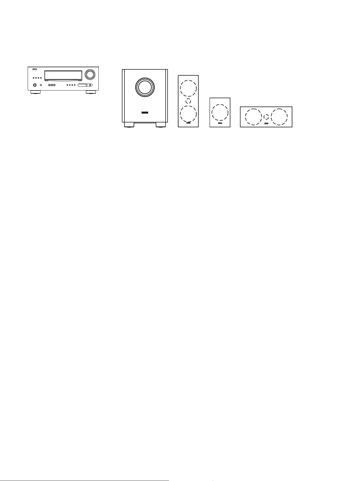
SYSTEM CONFIGURATION
• AVR-1311
• AVR-391
• DHT-1311XP (AVR-1311 + SYS-391HT)
• DHT-391XP (AVR-391 + SYS-391HT)
SYS-391HT : Refer to page 104-113 for the service manual.
TECHNICAL SPECIFICATIONS
n Audio Section
• Power amplifi er
Rated output :
Front :
75 W + 75 W (8 Ω, 20 Hz – 20 kHz with 0.08 % T.H.D.)
110 W + 110 W (6 Ω, 1 kHz with 0.7 % T.H.D.)
Center :
75 W (8 Ω, 20 Hz – 20 kHz with 0.08 % T.H.D.)
110 W (6 Ω, 1 kHz with 0.7 % T.H.D.)
Surround :
75 W + 75 W (8 Ω, 20 Hz – 20 kHz with 0.08 % T.H.D.)
110 W + 110 W (6 Ω, 1 kHz with 0.7 % T.H.D.)
Output connectors : 6 – 16 Ω
• Analog
Input sensitivity/Input impedance : 200 mV/47 kΩ
Frequency response: 10 Hz – 100 kHz — +1, –3 dB (DIRECT mode)
S/N : 98 dB (IHF–A weighted, DIRECT mode)
n Video Section
• Standard video connectors
Input/output level and impedance : 1 Vp-p, 75 Ω
Frequency response : 5 Hz – 10 MHz — +1, –3 dB
• Color component video connector
Input/output level and impedance :
Y (brightness) signal — 1 Vp-p, 75 Ω
B / CB signal — 0.7 Vp-p, 75 Ω
P
R / CR signal — 0.7 Vp-p, 75 Ω
P
Frequency response : 5 Hz – 10 MHz — +1, –3 dB
SYS-391HT
DSW-391 SC-C391SC-F391(x2) SC-R391(x2)
n Tuner section
[FM](Note: μV at 75 Ω, 0 dBf = 1 x 10
Receiving Range (for 391E3,391E3B) :
[FM] 87.5 MHz – 107.9 MHz
Receiving Range (for 1311E2,1311E1C,391EA) :
[FM] 87.5 MHz – 108.0 MHz
Usable Sensitivity :
[FM]1.2 μV (12.8 dBf)
50 dB Quieting Sensitivity :
[FM]MONO 2.8 μV (20.2 dBf)
S/N (IHF-A) :
[FM]MONO 70 dB
STEREO 67 dB
Total harmonic Distortion (at 1 kHz) :
[FM]MONO 0.7 %
STEREO 1.0 %
[AM]520 kHz – 1710 kHz
[AM]522 kHz – 1611 kHz
[AM]18 μV
n General
Power supply (for 391E3,391E3B) : AC 120 V, 60 Hz
(for 1311E2,391EA) : AC 230 V, 50 Hz
(for 1311E1C) : AC 220 V, 50 Hz
Power consumption :
330 W
Less than 0.5 W (Standby)
Maximum external dimensions :
435 (W) x 166 (H) x 381 (D) mm
Weight : 9.2 kg
n Remote Control Unit (RC-1149)
Batteries : R03/AAA Type (two batteries)
Maximum external dimensions : 50 (W) x 211 (H) x 22 (D) mm
Weight : 110 g (including batteries)
–15
W)
s
s
4
Page 5
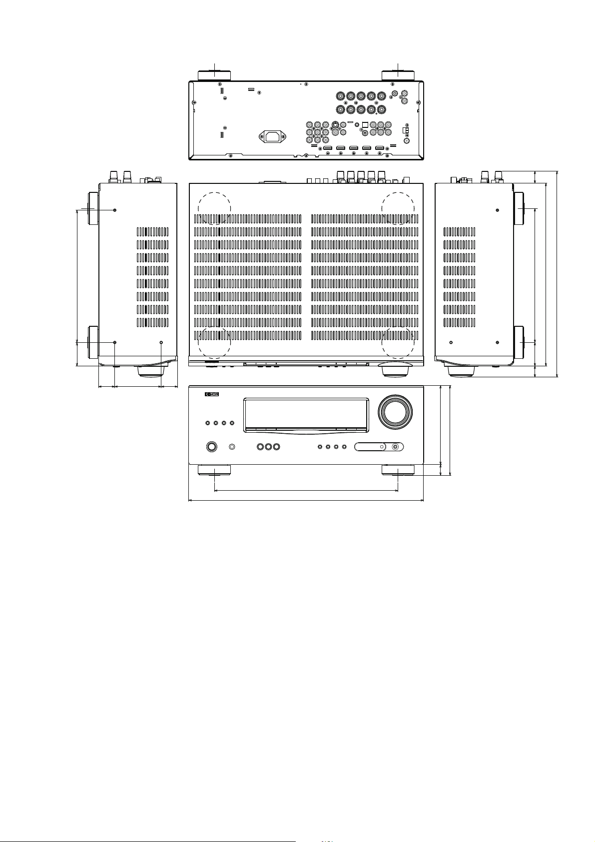
DIMENSION
22.2
245.0
43.5
30.0 30.5
86.0
340.0
435.0
248.0
43.5
20.7
146.5
166.5
20.0
The illustration is AVR-1311 model.
338.5
381.4
5
Page 6
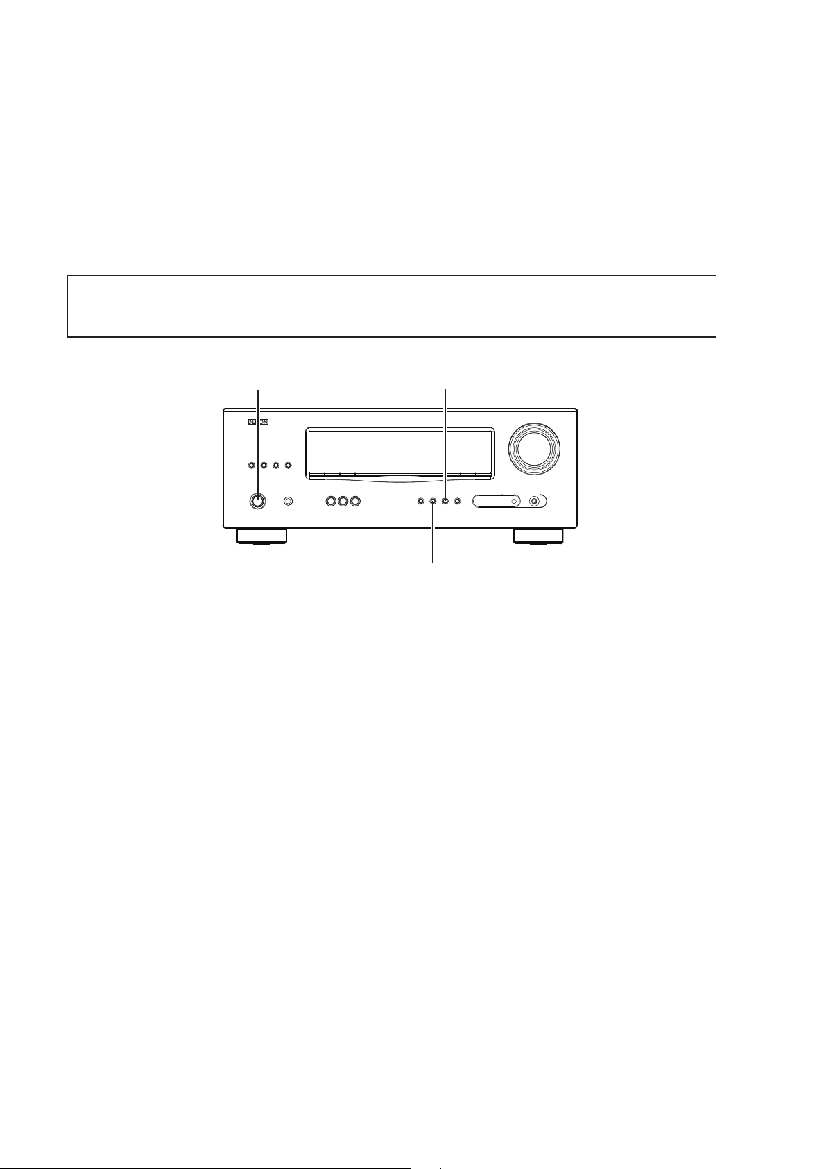
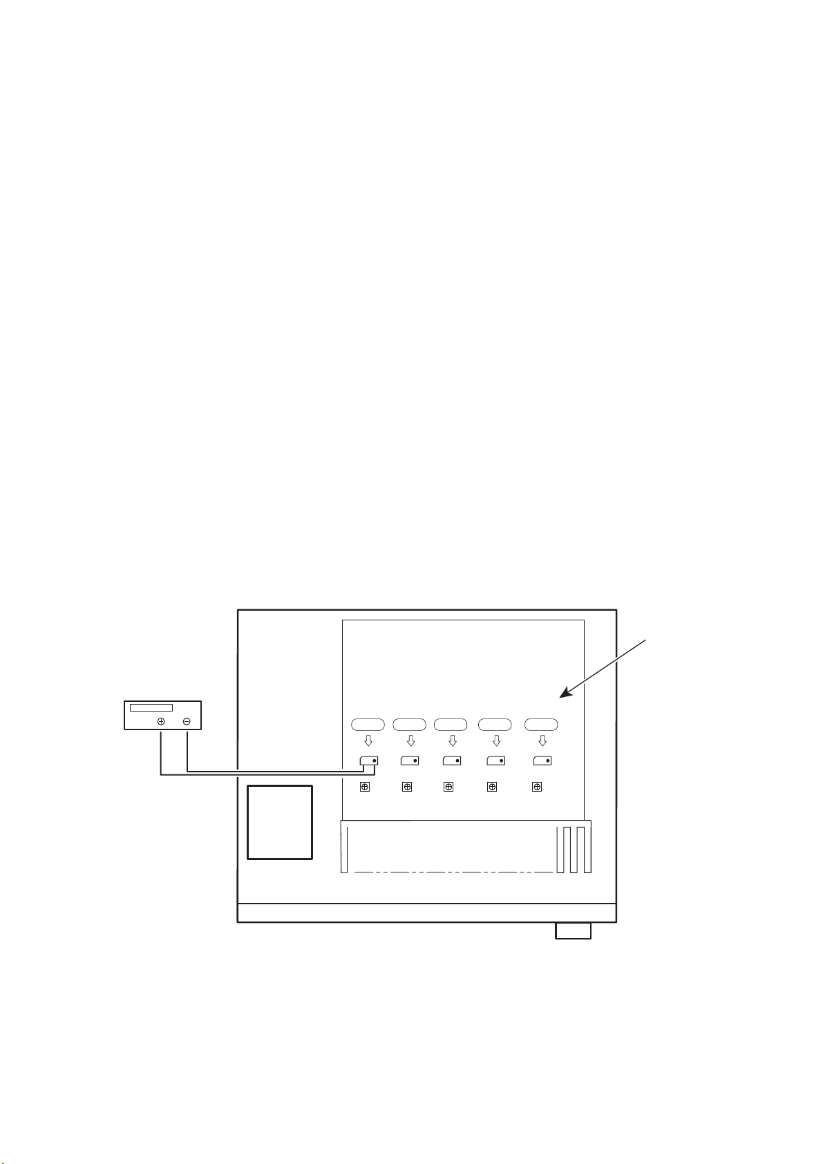
CAUTION IN SERVICING
Initializing AV SURROUND RECEIVER
AV SURROUND RECEIVER initialization should be performed when the μcom, peripheral parts of μcom, and Digital
P.W.B. are replaced.
1. Turn off the power using ON/STANDBY button.
2. Press ON/STANDBY button while simultaneously pressing SURROUND MODE 0 and SURROUND MODE
buttons.
3. Check that the entire display is fl ashing with an interval of about 1 second, and release your fi ngers from the 2
buttons and the microprocessor will be initialized.
Note: •If step 3 does not work, start over from step 1.
All user settings will be lost and this factory setting will be recovered when this initialization mode.
•
So make sure to memorize your setting for restoring after the initialization.
1
ON/STANDBY
SURROUND MODE 1
SURROUND MODE 0
Service Jigs
When you update the fi rmware, you can use the following
JIG (RS232C to internal connector conversion adapter with 4P FFC cable kit ).
Please order to Denon Offi cial Service Distributor in your region if necessary.
8U-210100S : WRITING KIT : 1 Set
606050028012P
(Refer to "VERSION UPGRADE PROCEDURE OF FIRMW
: 7P FFC(1.0) L-240 : 1 Set
ARE".)
6
Page 7
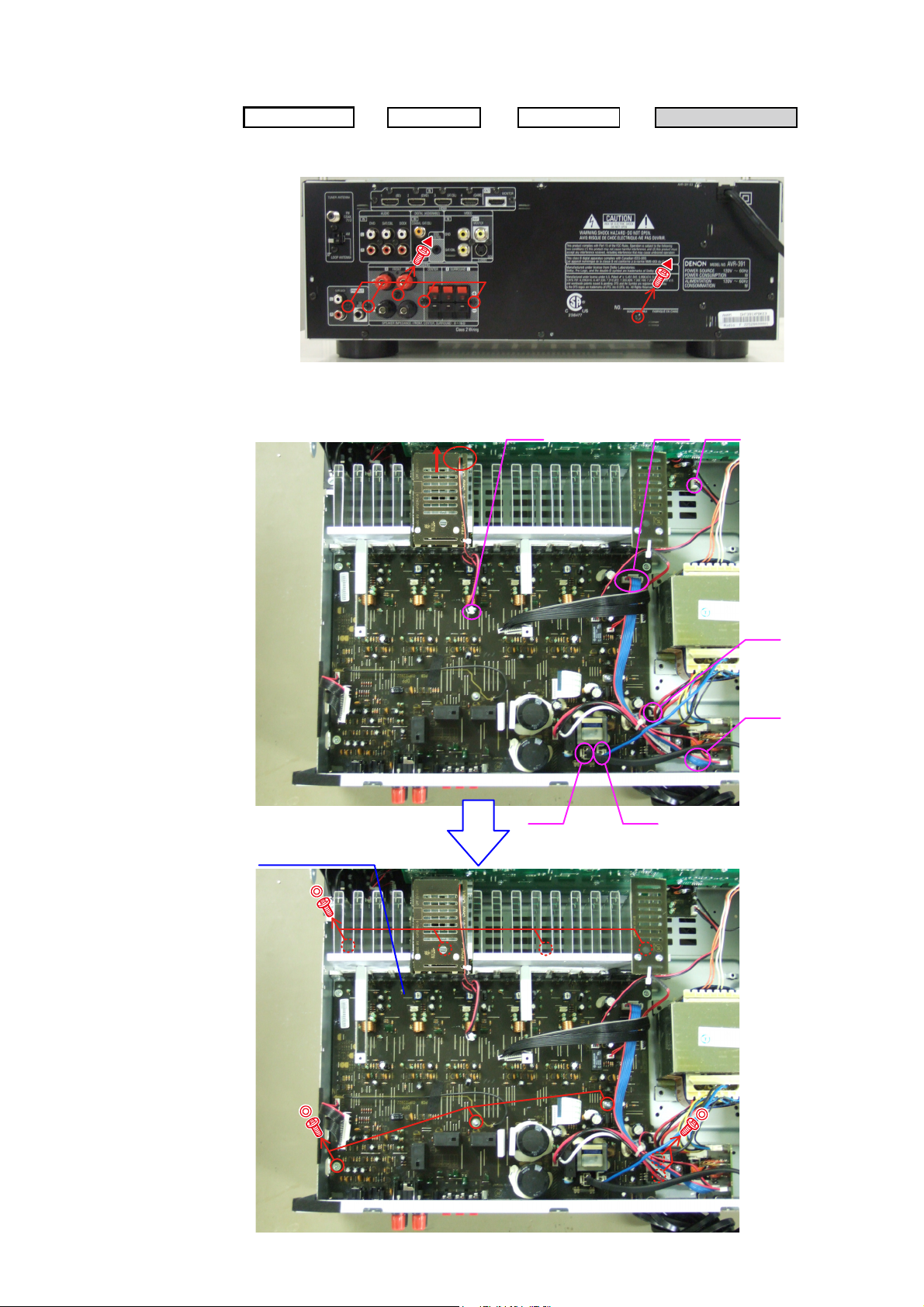
DISASSEMBLY
• Disassemble in order of the arrow of the fi gure of following fl ow.
• In the case of the re-assembling, assemble it in order of the reverse of the following fl ow.
• In the case of the re-assembling, observe "attention of assembling" it.
• If wire bundles are untied or moved to perform adjustment or parts replacement etc., be sure to rearrange them neatly
as they were originally bundled or placed afterward.
Otherwise, incorrect arrangement can be a cause of noise generation.
TOP COVER
FRONT PANEL ASSY
Refer to "DISASSEMBLY
1. FRONT PANEL ASSY"
and "EXPLODED VIEW"
AUX UNIT
(Ref. No. of EXPLODED VIEW : C1)
PHONE UNIT
(Ref. No. of EXPLODED VIEW : C2)
VOLUME UNIT
(Ref. No. of EXPLODED VIEW : C3)
HEADPHONE UNIT
(Ref. No. of EXPLODED VIEW : C8)
POWER UNIT
(Ref. No. of EXPLODED VIEW : C9)
FRONT UNIT
(Ref. No. of EXPLODED VIEW : C10)
HDMI UNIT
Refer to "DISASSEMBLY
2. HDMI UNIT"
and "EXPLODED VIEW"
HDMI UNIT
(Ref. No. of EXPLODED VIEW : C7)
INPUT UNIT
Refer to "DISASSEMBLY
3. INPUT UNIT"
and "EXPLODED VIEW"
INPUT UNIT
(Ref. No. of EXPLODED VIEW : C6)
RADIATOR ASSY
Refer to "DISASSEMBLY
4. RADIATOR ASSY"
and "EXPLODED VIEW"
MAIN UNIT
(Ref. No. of EXPLODED VIEW : C5)
REGULATOT UNIT
(Ref. No. of EXPLODED VIEW : C13)
POWER TRANS
(Ref. No. of EXPLODED VIEW : C14)
POWER UNIT
Refer to "DISASSEMBLY
5. POWER UNIT"
and "EXPLODED VIEW"
POWER TRANS
Refer to "DISASSEMBLY
6. POWER TRANS "
and "EXPLODED VIEW"
About the photos used for descriptions in the DISASSEMBLY" section.
• The direction from which the photographs used herein were photographed is indicated at "Direction of photograph: ***"
at the left of the respective photographs.
• Refer to the table below for a description of the direction in which the photos were taken.
• Photographs for which no direction is indicated were taken from above the product.
The viewpoint of each photograph
(Photografy direction)
[View from above]
Direction of photograph: C
Direction of photograph: B
Front side
Direction of photograph: D
Direction of photograph: A
7
Page 8

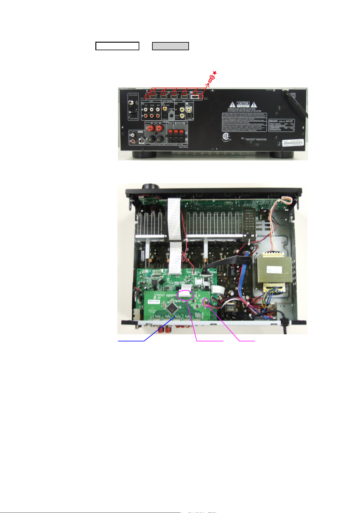
1. FRONT PANEL ASSY
Proceeding :
(1) Remove the screws.
View from bottom
(2) Cut the wire clamp band, then disconnect the connector wires and FFC cable. Remove the screws.
TOPCOVER
FRONT PANEL ASSY
FRONT PANEL ASSY
→
FFC cable
CN44
cut
CN209
cut
(3) Remove the screws.
Please refer to "EXPLODED VIEW" for the disassembly method of each P.W.B included in FRONT PANEL ASSY.
CN71
8
WIRE SUPPORT UNIT
Page 9
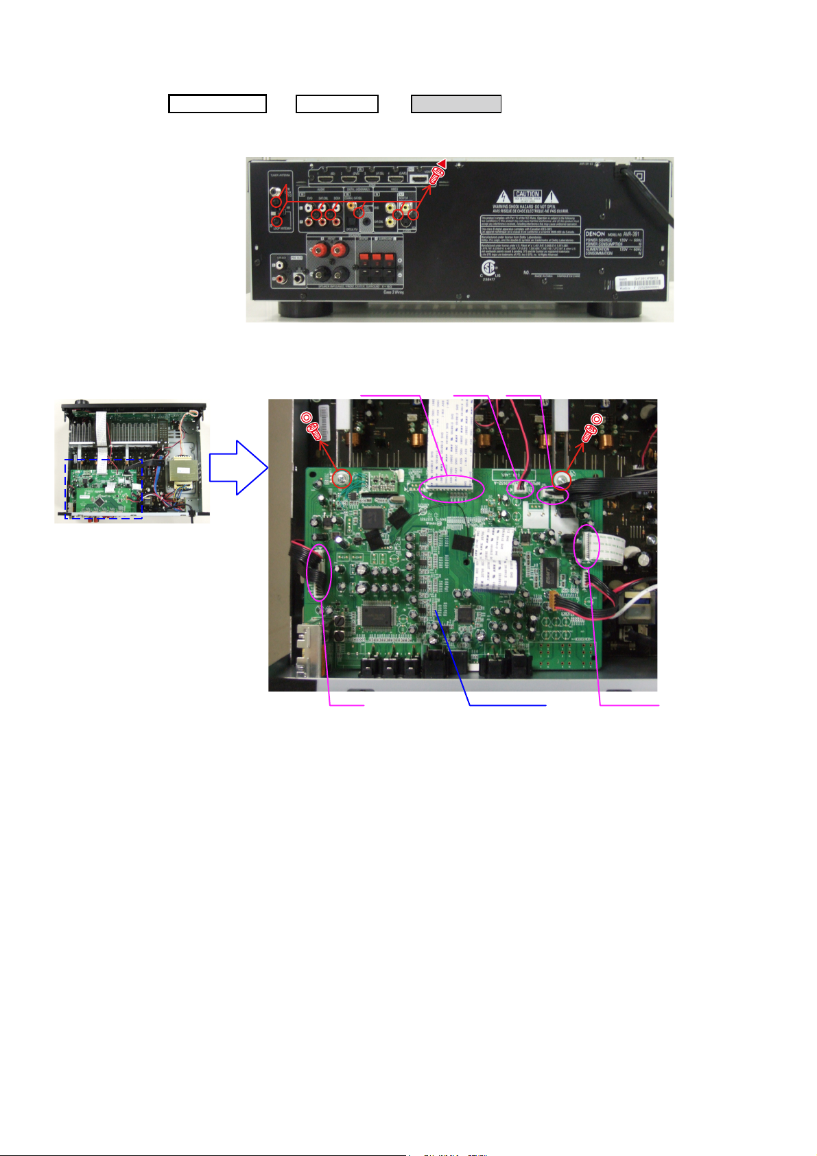
2. HDMI UNIT
Proceeding :
(1) Remove the screws.
Direction of photograph: A
(2) Disconnect the connector wire and FFC cable.
TOPCOVER
HDMI UNIT
→
HDMI UNIT
CN12FFC cable
9
Page 10
3. INPUT UNIT
Proceeding :
(1) Remove the screws.
Direction of photograph: A
(2) Disconnect the connector wires and FFC cables, then remove the screws.
TOPCOVER
HDMI UNIT
→
FFC cable
INPUT UNIT
→
CN71 CN43
CN42
INPUT UNIT
FFC cable
10
Page 11
4. RADIATOR ASSY
Proceeding :
(1) Remove the screws.
Direction of photograph: A
(2) Disconnect the connector wires, then remove the screws.
TOPCOVER
HDMI UNIT
→
→
INPUT UNIT
CN71 CN44
RADIATOR ASSY
→
CN46
RADIATOR ASSY
CN45
CN41
CN47 CN48
11
Page 12

(3) Remove the RADIATOR ASSY from the main unit.
Direction of photograph: C
Please refer to "EXPLODED VIEW" for the disassembly method of each P.W.B included in RADIATOR ASSY.
5. POWER UNIT
Proceeding :
Please refer to "EXPLODED VIEW" for the disassembly method of POWER UNIT.
TOPCOVER
POWER UNIT
→
6. POWER TRANS
Proceeding :
Please refer to "EXPLODED VIEW" for the disassembly method of POWER TRANS.
CABINET TOP
TRANS MAIN
→
12
Page 13
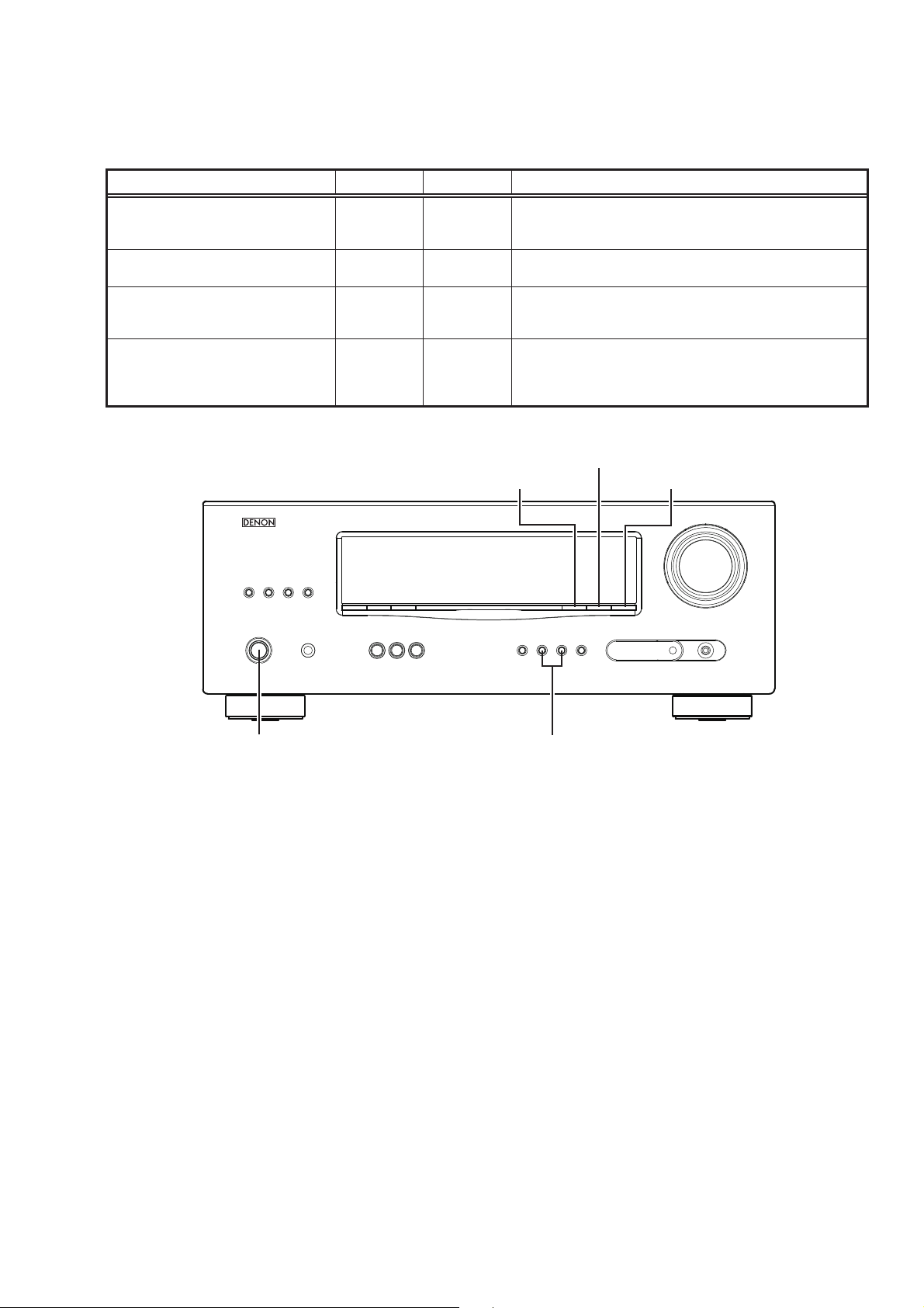
SPECIAL MODE
Special mode setting button
Press the ON/STANDBY button to turn on while pressing both buttons A and B at the same time.
b
Mode Button A Button B Contents
Firmware versions such as Main, DSP are displayed in the FL
μcom/DSP Version display mode STATUS DIMMER
Initialization mode
Mode for switching tuner frequency step
Mode for preventing remote control
acceptance
SURROUND
MODE
SURROUND
MODE
SURROUND
MODE
0
0
0
SURROUND
MODE
RESTORER
STATUS
display. Errors are displayed when they occur.
(Refer to page 14.)
Backup data initialization is carried out. (Refer to page 6.)
1
---E2 model only--Change tuner frequency step to AM9k/FM50kHz STEP or
AM:10k/FM:200kHz.
Operations using remote control are rejected.
"REMOTE LOCK:ON" is displayed in FL display.
(Mode cancellation: Turn off power and execute the same
button operations as when performing setup.)
DIMMER
RESTORER STATUS
ON/STANDBY
SURROUND
0 MODE 1
13
Page 14
1. μcom/DSP Version display mode
1.1. Operation specifi cations
μcom/DSP version display mode:
When started up, the version information is displayed.
Starting up:
With the "DIMMER" and "STATUS" buttons pressed, press the "ON/STANDBY" button to turn the power on.
Now, press the "STATUS" button to the display the 2nd item information on the FL Display.
1.2. Display Order
Model name → Main-μcom version → DSP version → iPod Dock version (Connecting iPod Dock)
Display State
AVR-391 E3 model
AVR-1311 E2 model
Model name
AVR-391 EA model
AVR-1311 E1C model
Main-μcom version
DSP version
iPod Dock (ASD-1R/11R)
iPod Dock (ASD-3/51)
Cleared of mode:
Press the "ON/STANDBY" button to turn the power off.
AVR391 E3
AVR1311 E2
AVR391 EA
AVR1311 E1C
Main **.**
DSP.*.*.*
Dock Ver :**.**
Dock :I********
1.3. Error display
See the following table for each "Error information" display and its contents (status).
Condition - State
DSP NG When DSP boot, executing DSP reset makes to becomes error.
DSP OK (No error display, version display only)
DSP ERROR 01
14
Page 15
ABOUT REPLACE THE MICROPROCESSOR WITH A NEW ONE
When replaced of the U-PRO (Microprocessor) or the Flash ROM, conrm contents of the following.
PWB Name Ref. No. Description
DIGITAL IC91 T5CN5 B SOFTWARE: Main
DIGITAL IC82 ST25VF080B-50-4C-S2AF B SOFTWARE: DSP ROM
After
replaced
Remark
After replaced
A : Mask ROM (With software). No need write-in of software to the microprocessor.
B : Flash ROM (With software). Usually, no need write-in of software. But, when the software was updated, you should be
write-in of the new software to the microprocessor or ash ROM. Please check the software version.
C : Empty Flash ROM (Without software). You should be write-in of the software to the microprocessor or ash ROM.
Refer to "Update procedure" or "writing procedure", when you should be write-in the software.
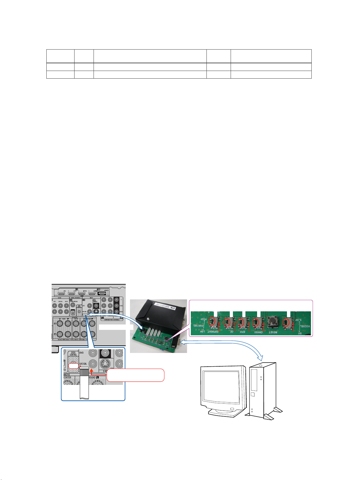
VERSION UPGRADE PROCEDURE OF FIRMWARE
1. Preparations
-Before starting the operation-
(1) Personal Computer (Installed “BootTool_M330(Writing program).exe”).
(2) RS-232 cable (9P (Male), Straight).
(3) 8U-210100S Writing Kit.
(4) 606050028012P / 7P FFC(1.0) L=240.
-Connection of the AV receiver-
(1) Conrm the power on/off switch of the AV receiver is turning off.
(2) Connect the update terminal of AV receiver with the “Writing Kit”.
(Refer to gure below for the connection of the 7P FFC cable.)
(3) Connect the RS-232C cable from PC with the “Writing Kit”.
7P FFC Cable
Writing Kit
1 pin
This side is contacts of
7P FFC Cable.
7P FFC Cable
S706-709 : HIGE
S709
S708
RS-232C Cable
S707
S706
S702 : 3.3V
S702
PC
15
Page 16

2. UPDATE FIRMWARE
(1) Connect the update terminal of AV receiver with the “Writing Kit”.
(2) Set the switch of “Writing Kit" (Refer to the table below).
DSPBOOT CE EPM CNVSS
H H H H
(3) Press the "ON/STANDBY" button to turn the power on of AV receiver.
(4) Set the switch of “Writing Kit" (Refer to the table below).
DSPBOOT CE EPM CNVSS
H H L H
(5) Press the "RESET" switch of “Writing Kit".
(6) Run the “BootTool_M330(Writing program).exe” on desktop of PC.
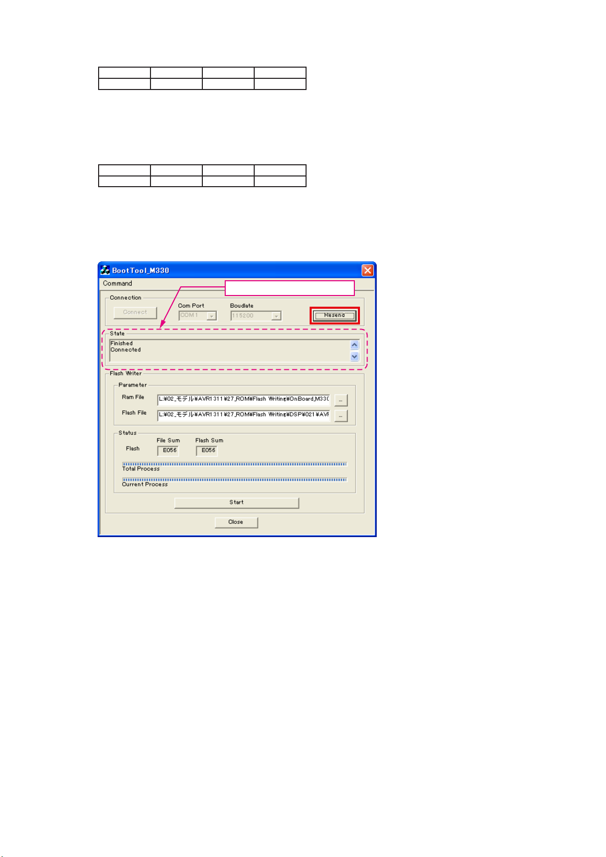
(7) Click the “Connect” button.
"Connected" is displayed, it is OK.
16
Page 17
DSP SF1
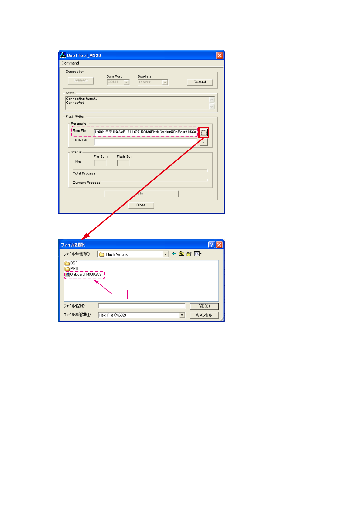
(8) Choose Ram File(OnBoard_M330.s32).
Choose Ram File(OnBoard_M330.s32).
17
Page 18
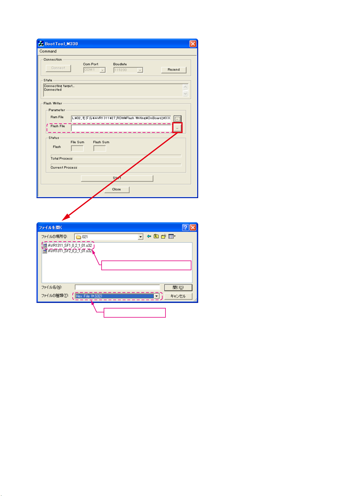
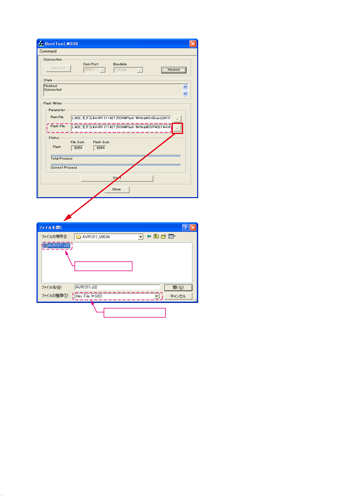
(9) Choose Flash File(DSP : SF1).
Choose "AVR1311_SF1_*_*_*_01.s32".
Choose "Hex File (*.S32)".
18
Page 19
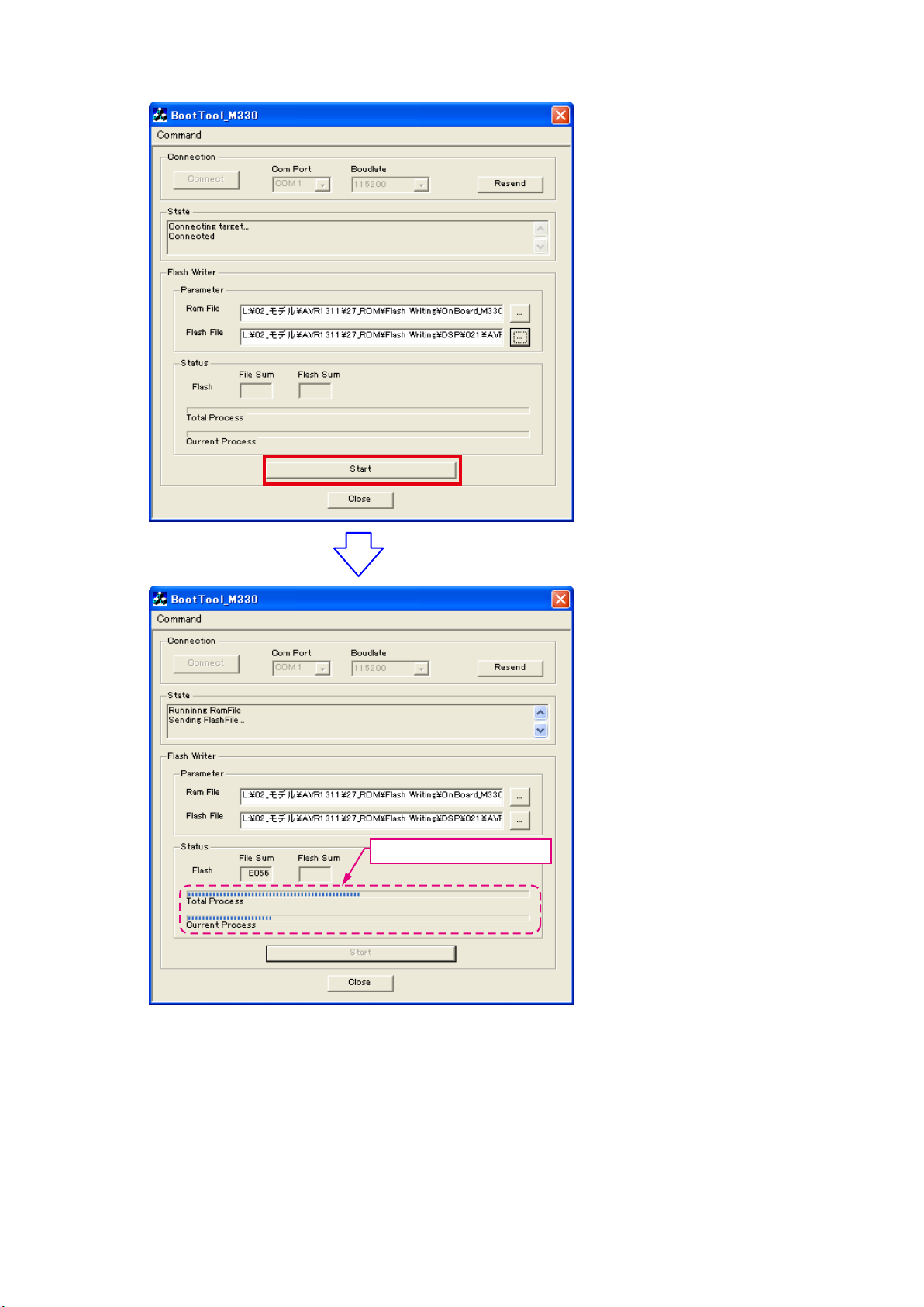
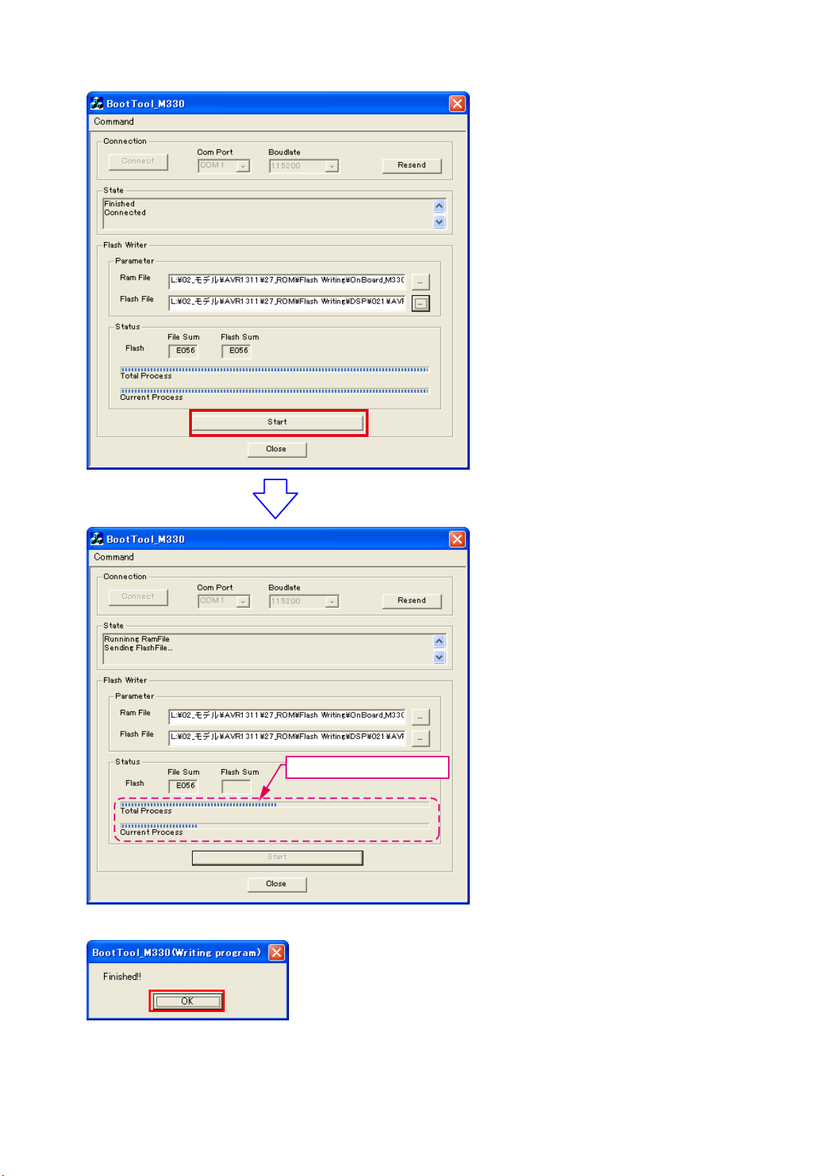
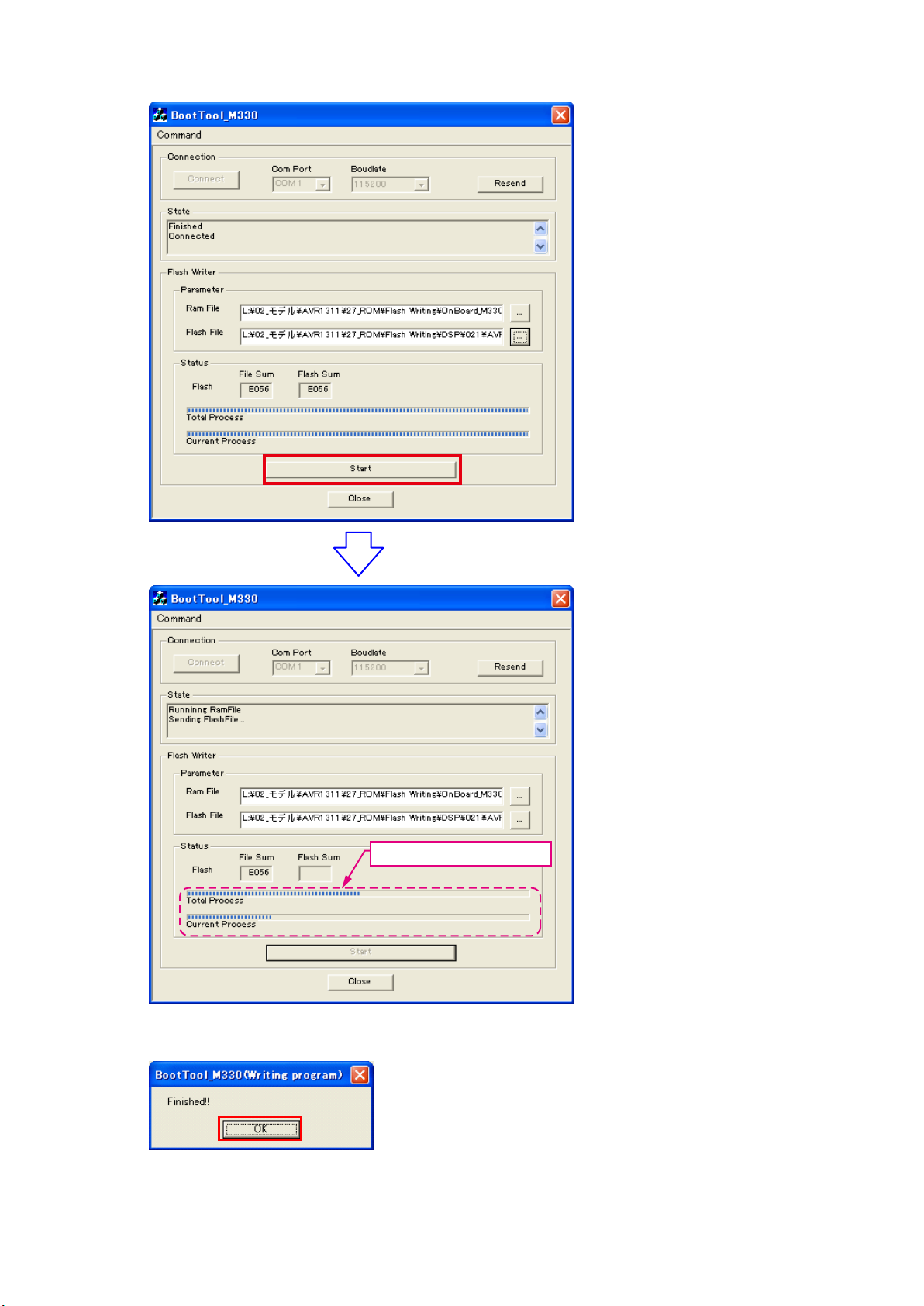
(10) Click the “Start” button.
The Setup Status bar appears.
19
Page 20
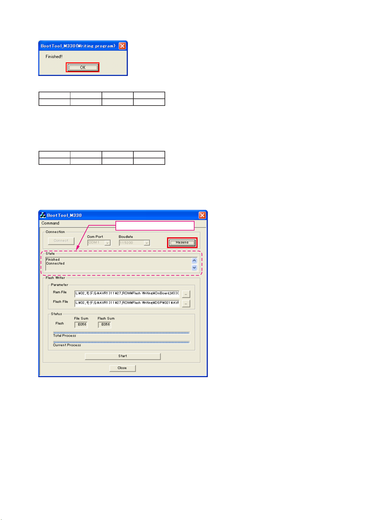
(11) "Finished!!" is displayed. Click the "OK"” button.
(12) Set the switch of “Writing Kit" (Refer to the table below).
DSPBOOT CE EPM CNVSS
H H H H
(13) Press the "RESET" switch of “Writing Kit".
(14) AV receiver is power on and starts update of DSP1.
(15) "Write Comleted" is displayed in the FL tube.
(16) Set the switch of “Writing Kit" (Refer to the table below).
DSPBOOT CE EPM CNVSS
H H L H
(17) Press the "RESET" switch of “Writing Kit".
DSP SF2
(18) Click the “Resend” button.
"Connected" is displayed, it is OK.
20
Page 21

(19) Choose Flash File(DSP : SF2).
Choose "AVR1311_SF2_*_*_*_01.s32".
Choose "Hex File (*.S32)".
21
Page 22
(20) Click the “Start” button.
The Setup Status bar appears.
(21) "Finished!!" is displayed. Click the "OK"” button.
22
Page 23
(22) Set the switch of “Writing Kit" (Refer to the table below).
DSPBOOT CE EPM CNVSS
H H H H
(23) Press the "RESET" switch of “Writing Kit".
(24) AV receiver is power on and starts update of DSP2.
(25) "Write Comleted" is displayed in the FL tube.
(26) Set the switch of “Writing Kit" (Refer to the table below).
DSPBOOT CE EPM CNVSS
H H L H
(27) Press the "RESET" switch of “Writing Kit".
MAIN
(28) Click the “Resend” button.
"Connected" is displayed, it is OK.
23
Page 24
(29) Choose Flash File(MAIN).
Choose "AVR1311.s32".
Choose "Hex File (*.S32)".
24
Page 25
(30) Click the “Start” button.
The Setup Status bar appears.
(31) "Finished!!" is displayed. Click the "OK"” button.
25
Page 26
(32) Set the switch of “Writing Kit" (Refer to the table below).
DSPBOOT CE EPM CNVSS
H H H H
(33) Press the "RESET" switch of “Writing Kit".
(34) Initializing.
1. Turn off the power using ON/STANDBY button.
2. Press ON/STANDBY button while simultaneously pressing SURROUND MODE
and SURROUND MODE
0
buttons.
3. Check that the entire display is ashing with an interval of about 1 second, and release your ngers from the 2
buttons and the microprocessor will be initialized.
Note: •If step 3 does not work, start over from step 1.
All user settings will be lost and this factory setting will be recovered when this initialization mode.
•
So make sure to memorize your setting for restoring after the initialization.
3. Notice:
Please keep the following notice for rmware update.
(a) Keep the PC environment
(b) Avoid the communication cable from the electrical noise source.
(e.g. telephone cable, AC line, a uorescent light)
(c) Don’t remove cable during update.
(d) Don’t turn off the power during update.
(e) Don’t run other PC application during update.
(f) Stop the resident program on PC (Virus checker and System check utilitu, etc)
(g) Stop the screen saver on PC.
(h) Stop the power save ability on PC.
(i) In case of laptop PC, Use the AC adaptor.
1
Conrming the rmware’s number after upgraded
After completion of the updating operation, the new version number can conrmed by starting up the AVR1311 or AVR391
according to the following procedure.
With the following operation, the AVR1311 or AVR391 can be set to the Flash ROM Version-Number Conemation mode.
Turn on power switch while simultaneously pressing "DIMMER" and "STATUS" buttons on the front panel. Every time the
"STATUS" button is pressed, version number of the Model, Main, DSP, … are indicated on the front panel section in the
following order.
Depression Button Name Remarks
1 STATUS Model Name AVR1311 or AVR391 **
2 STATUS Main CPU Main: **.**
3 STATUS DSP ROM DSP.*.*.*
26
Page 27
ADJUSTMENT
Audio Section
Idling Current
Required measurement equipment: DC Voltmeter
1. Preparation
(1) Avoid direct blow from an air conditioner or an electric fan, and adjust the unit at normal room temperature
15 °C ~ 30 °C.
(2) Presetting
• POWER (Power source switch) OFF
• SPEAKER (Speaker terminal) No load
(Do not connect speaker, dummy resistor, etc.)
2. Adjustment
(1) emoved top cover and set VR41(FL),VR45(FR),VR42(C),VR44(SL),VR43(SR), on Main Amp. Unit at fully
counterclockwise position.
(2) Connect DC Voltmeter to test points (Front-Lch:CN51,Front-Rch:CN55,CENTERch:CN53,
Surround-Lch:CN52,Surround-Rch:CN54).
(3) Connect power cord to AC Line, and turn power switch "ON".
(4) Presetting.
MASTER VOLUME : "---" counterclockwise (c min.)
SPEAKER (Speaker terminal) : No load
(Do not connect speaker, dummy resistor, etc.)
FUNCTION : DVD
(5) Within 2 minutes after the power on, turn VR41 clockwise (x) to adjust the TEST POINT voltage to
1.5 mV ± 0.5 mV DC.
(6) After 10 minutes from the preset above, turn VR401 to set the voltage to 2.0 mV ± 0.5 mV DC.
(7) Adjust the Variable Resisters of other channels (VR42-VR45) in the same way.
DC Voltmeter
S Lch
F Lch
CN51
VR41 VR44 VR42 VR43 VR45
CN52
C ch
CN53
S Rch
CN54
F Rch
CN55
MAIN UNIT ASS'Y
27
Page 28
SURROUND MODES AND PARAMETERS
SS
D. Comp z3 DRCz4 LFE z5
z2
DSSS
z1
Channel output Surround Parameter
SS
z2
SDD D DSSS
SDD D D S S
SDD D D S S
SDD D D S
SDD D D S S
SDD D D S S
SDD D D S S
SDD D D S S
SDD D D S S
SDD D D S
S DSSS
SDD D
S D
Front L/R Center Surround L/R Surround Back L/R Subwoofer Mode
Surround mode
DTS NEO:6
DOLBY DIGITAL
DOLBY DIGITAL Plus
DOLBY TrueHD
DTS SURROUND
DTS 96/24
MULTI CH IN
DOLBY PRO LOGIC gx SDD D DSSS
STEREO
DIRECT (Multi-channel)
Symbols in the table
S This indicates the audio output channels or surround parameters that can be set.
D This indicates the audio output channels. The output channels depend on the settings of “Speaker Config.”.
DIRECT (2channel)
DOLBY PRO LOGIC g S D D DSSS
DTS-HD
S D
DTS Express
MULTI CH STEREO
VIRTUAL
z1 A signal for each channel contained in an input signal is output as audio.
z2 Only when “Mode” is set to “LFE+Main”, sound is output from the subwoofer.
z3 This item can be selected when a Dolby Digital or DTS signal is played.
z4 This item can be selected when a Dolby TrueHD signal is played.
z5 This item can be selected when a Dolby Digital or DTS signal or DVD-Audio is played.
28
Page 29
RESTORER z7
Tone
NEO:6 Music mode only
PRO LOGIC g/gx Music mode only
Panorama Dimension Center Width Center Image
Surround Parameter
SS
SS
z2
S
S.Back Subwoofer
AFDM z6
Surround mode
DIRECT (2 channel)
SS S
DIRECT (Multi-channel)
STEREO
MULTI CH IN
DOLBY PRO LOGIC gx S SSS SS
DOLBY PRO LOGIC g S SSS SS
S SSS
SS S
SS S
SS
SS S
SS S
DOLBY DIGITAL
DOLBY DIGITAL Plus
DOLBY TrueHD
DTS SURROUND
DTS NEO:6
DTS 96/24
S SS
SS
SS S
z2 Only when “Mode” is set to “LFE+Main”, sound is output from the subwoofer.
z6 This item can be selected when a Dolby Digital or DTS or DVD-Audio signal is played.
z7 This item can be set when the input signal is analog, PCM 48 kHz or 44.1 kHz.
DTS-HD
DTS Express
MULTI CH STEREO
VIRTUAL
29
Page 30

DOLBY
DIGITAL
DOLBY
DIGITAL
(2ch)
(4/3ch)
DOLBY
DIGITAL
(5.1/5/4ch)
Flag)
DOLBY
(With no
DIGITAL EX
DOLBY
(With Flag)
DIGITAL EX
DOLBY
DIGITAL Plus
DOLBY
TrueHD
DTS 96/24
DTS
(5.1ch)
Input signal types and formats
MTRX
DTS ES
DSCRT
DTS ES
(With Flag)
(With Flag)
F
SSF
S S
DS
SFFF
F
DTS
EXPRESS
High
DTS-HD
Resolution
Audio
Master
DTS-HD
(2ch)
LINEAR PCM
PCM DTS-HD DTS DOLBY DOLBY DIGITAL
(multi ch)
LINEAR PCM
ANALOG
Audio
F
F
F
SS S
SS S
z F D
z F D
z SSS
z SSSS
SS S
z If “Speaker Config.“ – “S.B(Pre)“ is set to “None”, this surround mode cannot be selected.
Surround mode NOTE
DTS NEO:6 CINEMA
DTS NEO:6 MUSIC
DTS-HD MSTR
DTS-HD HI RES
DTS ES DSCRT6.1
DTS ES MTRX6.1
DTS SURROUND
DTS 96/24FDTS + PLgx CINEMA z SSSS
DTS + PLgx MUSIC z SSSS
DTS EXPRESS
DTS + NEO:6
Symbols in the table
F This indicates the default surround mode.
D This indicates the surround mode that is fixed when “AFDM” is set to “ON”.
S This indicates the selectable surround mode.
DTS SURROUND
DOLBY TrueHD
DOLBY SURROUND
30
DOLBY DIGITAL+
DOLBY DIGITAL EX
DOLBY DIGITAL
DOLBY (D) +PLgx CINEMA z F
DOLBY (D) +PLgx MUSIC z SSSS
DOLBY PRO LOGIC gx CINEMA zS S S
DOLBY PRO LOGIC gx MUSIC zS S S
DOLBY PRO LOGIC gx GAME zS S S
DOLBY PRO LOGIC g CINEMA SS S
DOLBY PRO LOGIC g MUSIC SS S
DOLBY PRO LOGIC g GAME SS S
DOLBY PRO LOGIC
Page 31

DOLBY
DIGITAL
DOLBY
DIGITAL
DOLBY
DIGITAL
DOLBY
DIGITAL EX
DOLBY
DIGITAL EX
DOLBY
DOLBY
DTS 96/24
DTS
(2ch)
(4/3ch)
(5.1/5/4ch)
Flag)
(With no
(With Flag)
DIGITAL Plus
TrueHD
(5.1ch)
Input signal types and formats
MTRX
DTS ES
(With Flag)
DSCRT
DTS ES
(With Flag)
DTS
EXPRESS
High
DTS-HD
Resolution
Audio
Master
DTS-HD
(2ch)
LINEAR PCM
PCM DTS-HD DTS DOLBY DOLBY DIGITAL
(multi ch)
LINEAR PCM
ANALOG
Audio
F
F D (7.1)
SS S SSSSSSSSSSSSSS
SS S SSSS SSSSS
SS S SSSS SSSSS
FS F SSSSSSSSSSSSSS
z If “Speaker Config.“ – “S.B(Pre)“ is set to “None”, this surround mode cannot be selected.
Surround mode NOTE
MULTI CH IN
MULTI CH IN + PLgx CINEMA zS
MULTI CH IN + PLgx MUSIC zS
MULTI CH IN 7.1
DIRECT
MULTI CH STEREO
VIRTUAL
STEREO
MULTI CH IN
DIRECT
DSP SIMULATION
STEREO
31
Page 32

TROUBLE SHOOTING
1. POWER
1.1. Power not turn on
Power not turn on.
Is the ON/STANDBY
indicator on the front panel
fl ashing red?
YES
Are there any incomplete
connections in the
connectors connecting
between the various circuit
boards?
Is there a short circuit
NO
between the speaker
terminals and the ground?
Correct the short
YES
circuit between the
speaker and ground.
NO
Is the fuse blown?
NO
Does the power turn on
when the POWER switch is
turned off then back on?
YES YES YES
Check the primary ciruitry
parts including the POWER
switch(for poor contacts,
etc.), and replace any
defective parts.
YES
Connect the connectors
property.
YES
Refer to Fuse is blown.
Is a DC 5V voltage being
NO NO
supplied from the MAIN B'd
to the microprocessors?
Check the microprocessor
periphery circuitry and
replace any degective parts.
NO
Check for damage in the
power amplifi er circuitry
parts and replace any
defective parts.
Is a DC5V voltage output
when the cord supplying the
power from the MAIN B'd to
the microprocessor(BN43)
is unplugged?
Check the circuitry and parts
from BN43 on the MAIN
B'd to the microprocessor
for damage and shortcircuits,and replace any
defective parts.
Check the parts from
NO
IC45 to the primary
circuitry and replace
any defective parts.
1.2. Fuse is blown
Check for leaks or short
circuits in the primary side
parts,and replace any
defective parts.
Fuse is blown
Check for short circuits in the
rectifi er diodes and circuitry of
the secondary side rectifying
circuits,and replace any
defective parts.
After repairing, also replace the fuse.
32
Check for short circuits in
the power stabilizer unit's
regulator output terminal and
the ground,and replace any
defective parts.
Page 33

2. Analog video
MONITOR OUT(CVBS) Output NG
Check ±5V
+5V : C755
-5V : C754
OK
Check output
Output V : IC71-1pin
OK
Check cable between main unit and monitor
or Check monitor.
AVR-1311 model only
MONITOR OUT(COMPONENT) Output NG
Check ±5V
+5V : C797
-5V : C799
OK
Check output
Output Y : C785
Output Pb : C787
Output Pr : C789
NG
The power supply circuitry is defective.
NG
The IC71 and surrounding circuitry is defective.
NG
The power supply circuitry is defective.
NG
The IC73 and surrounding circuitry is defective.
OK
Check cable between main unit and monitor
or Check monitor.
33
Page 34

3. HDMI/DVI
3.1. No picture or sound is output
No picture or sound is output.
Check HDMI/DVI cable connection.
(1) Is the HDMI/DVI cable properly connected?
YES
(2) Are you using an HDMI/DVI selector, repeater or a device for
improving picture quality?
YES
(3) Are you using a certifi ed HDMI cable (one with the HDMI stamp)?
YES
(3) Are you using an HDMI/DVI cable less than 5 meters in length?
YES
(4) Are the picture and sound output when another HDMI/DVI cable
is used?
NO
NO
There may be a problem with the HDMI/DVI
cable. Check connection.
YES
Disconnect everything and connect only the
HDMI/DVI cable to check
NO
Use a certifi ed HDMI cable (one with the
HDMI stamp).
Replace the HDMI/DVI cable with one that
NO
is less than 5 meters in length (2 meters
recommended) to check.
YES
The HDMI/DVI cable is defective.
Check BD/DVD player.
YES
(5) Is the BD/DVD player's HDMI output setting correct?
YES
(6) When using a DENON BD/DVD player's, is the fl uorescent
display tube's "HDMI" indicator lit? If using a non-DENON BD/
DVD player's, proceed to
NO
(8) Is sound output from the set's speaker terminals when the TV's
power is turned off or the connection cable between the TV and
the set is disconnected?
"YES".
YES
(7)
Are the picture and sound output
when the BD/DVD player's
resolution is changed?
NO
NO
(9) Are the picture and sound
output when a different BD/
DVD player's is used?
NO
YES
Check HDMI output setting, referring to the
BD/DVD player's operating instructions.
YES
Set the BD/DVD player's output resolution to
a resolution with which the TV is compatible.
YES
The BD/DVD player's may not be compatible
with HDCP repeaters. Ask the BD/DVD
player's manufacturer.
YES
The BD/DVD player's is defective.
34
Page 35

Check TV
(10) Is the TV HDCP-compatible?
YES
(11) Is the TV compatible with resolutions of 1080P?
YES
(12) Is the TV's input set to HDMI?
YES
(13) Are the picture and sound output when a different TV is used?
Check set (AVR-1311, 391)
(14) Is the set's input set to HDMI?
YES
YES
NO
Use an HDCP-compatible TV. PC TVs
cannot be used.
If the TV is not compatible with resolutions
NO
of 1080P, no picture will be output, even
if the BD/DVD player's resolution is set to
1080P.
NO
Check TV's input setting, referring to the
TV's operating instructions.
NO
The TV is defective.
NO
Check set's input setting, referring to the
set's operating instructions.
The set does not recognize the TV.
(15) Is the "H"(3V-5V) signal outputted of IC11 (41pin)?
With the TV connected, Check voltage of the IC on the side on
which the TV is connected.
Is communication waveform confi rmed in 15pin(DDC_
CLK)/16pin(DDC_DATA)
Is terminate the TMDS signal
6pin/7pin/9pin/10pin/12pin of HDMI connector (JK15)?
YES
(16)
When using a DENON
BD/DVD player, is the FL
display's "HDMI" indicator lit?
If using a non-DENON BD/
DVD player, proceed to
"NO".
YES
of HDMI connector (JK15)
is
3.3V
confi rmed in
The BD/DVD player does not recognize the
connection with the set.
(17)
Is the "H"(3V-5V) signal outputted of HDMI
connector (JK11/JK12/JK13/JK14 : 19pin)?
NO NO
With the BD/DVD player connected, Check
voltage of the HDMI connector for the input
on the side on which the BD/DVD player is
connected.
Is communication waveform confi rmed in
15pin(DDC_CLK)/16pin(DDC_DATA)
HDMI connector
Is terminate the TMDS signal
1pin/3pin/4pin/6pin/7pin/9pin/10pin/12pin of each
HDMI connector?
?
1pin/3pin/4pin/
YES
YES
The pattern and circuit from the HDMI
NO
connector (JK15) to the IC11 is defective, or
HDMI output circuitry is defective (IC11 and
surrounding circuitry).
The pattern and circuit
from the HDMI connector
(JK11/JK12/JK13/JK14)
to the IC11 is defective.
of each
?
is
3.3V
confi rmed in
Check operation of IC11.
(Video input 480P from BD/DVD players / Connect the TV.)
(18) Check power supply.
Are 1.8V or 3.3V supplied to IC11 (each power supply pin)?
YES
NO
The power supply circuitry is defective.
35
Page 36

(19) Check xtal oscillator.
Is there 28.6363MHz oscillation of X101?
NO
The X101 or IC11 is defective.
YES
(20) Check RESET.
Is RESET waveform confi rmed in IC11 (97pin), when power is
turned on? (If continued to "H" or " L", proceed to "NO".)
YES
(21) Check control signal(I2C).
Is waveform confi rmed in IC11 78pin(SDATA)/79pin(SCL). (If not
continued to " L", proceed to "YES".)
YES
HDMI output circuitry is defective (IC11 and surrounding circuitry).
NO
The RESET pattern or IC11 is defective.
NO
The SDATA/SCL line pattern is defective.
36
Page 37

3.2. HDMI test point and waveforms
Detail
+5V
A
D
A
TMDS D2+ HPD
TMDS D0+
TMDS D2-
TMDS D0-
B
C
B
Detail
TMDS D2- TMDS D0-
TMDS D2+ TMDS D0+ HPD
C
Detail
43pin㧦DDC_DATA
44pin㧦DDC_CLK
TMDS D1+ TMDS D1+
TMDS D1- TMDS D1-
DDC_DATA DDC_CLK
TMDS D1+ +5VTMDS CK+
TMDS D1- TMDS CK-
D
Detail
HDMI_SCL HDMI_SDA
37
Page 38

DDC_CLK/DDC_DATA/TMDS : Check item (15),(17)
0.9V
DDC_CLK
TMDS SIGNAL
2.48V
IPINDE/IPINVSYNC/IPINHSYNC/IPINPCK : Check item (21)
HDMI_SDA
HDMI_SCL
DDC_DATA
38
Page 39

CLOCK FLOW & WAVE FORM IN DIGITAL BLOCK
䇭
㩿㪏㪎㪀㪘㪧㪇㪶㪦㪬㪫
㩿㪏㪏㪀㪘㪧㪈㪶㪦㪬㪫
㩿㪏㪐㪀㪘㪧㪉㪶㪦㪬㪫
㩿㪐㪇㪀㪘㪧㪊㪶㪦㪬㪫
㩿㪐㪈㪀㪘㪧㪋㪶㪦㪬㪫
㩿㪐㪋㪀㪘㪧㪌㪶㪦㪬㪫
㩿㪐㪌㪀㪪㪚㪣㪢㪶㪦㪬㪫
㩿㪐㪍㪀㪤㪚㪣㪢㪶㪦㪬㪫
㪛㪘㪠㪈㪶㪛㪘㪫㪘㪇㪃㪛㪪㪛㪇㩿㪉㪎㪀
㪛㪘㪠㪈㪶㪛㪘㪫㪘㪈㪃㪛㪪㪛㪈㩿㪉㪍㪀
㪛㪘㪠㪈㪶㪛㪘㪫㪘㪉㪃㪛㪪㪛㪉㩿㪉㪋㪀
㪛㪘㪠㪈㪶㪛㪘㪫㪘㪊㪃㪛㪪㪛㪊㩿㪉㪊㪀
㪛㪘㪠㪈㪶㪣㪩㪚㪢㪃㪛㪪㪛㪋㩿㪊㪇㪀
㪛㪘㪠㪈㪶㪪㪚㪣㪢㪃㪛㪪㪛㪄㪚㪣㪢㩿㪉㪐
㪀
㪛㪘㪦㪶㪤㪚㪣㪢㩿㪋㪇㪀
㩿㪋㪎㪀㪛㪘㪦㪈㪶㪛㪊
㩿㪋㪏㪀㪛㪘㪦㪈㪶㪛㪉㪃㪟㪪㪉
㩿㪋㪐㪀㪛㪘㪦㪈㪶㪛㪘㪫㪘㪈㪃㪟㪪㪈
㩿㪌㪈㪀㪛㪘㪦㪈㪶㪛㪘㪫㪘㪇㪃㪟㪪㪇
㩿㪌㪉㪀㪛㪘㪦㪈㪶㪪㪚㪣㪢
㩿㪌㪋㪀㪛㪘㪦㪈㪶㪣㪩㪚㪣㪢
㩿㪈㪍㪀㪯㪫㪘㪣㪶㪦㪬㪫
㩿㪊㪉㪀㪛㪘㪠㪉㪶㪣㪩㪚㪢
㩿㪊㪊㪀㪛㪘㪠㪉㪶㪪㪚㪣㪢
㩿㪊㪋㪀㪛㪘㪠㪉㪶㪛㪘㪫㪘㪃㪛㪪㪛㪌
㪪㪘㪠㪶㪚㪣㪢㩿㪍㪈㪀
㪪㪘㪠㪶㪣㪩㪚㪢㩿㪍㪇㪀
㪪㪘㪠㪶㪪㪛㪦㪬㪫㩿㪌㪋㪀
㪩㪤㪚㪢㩿㪌㪌㪀
㩿㪈㪀㪚㪯㪶㪪㪛㪠㪥㪈
㩿㪍㪋㪀㪚㪯㪶㪪㪛㪠㪥㪉
㩿㪍㪊㪀㪚㪯㪶㪪㪛㪠㪥㪊
㩿㪍㪉㪀㪚㪯㪶㪪㪛㪠㪥㪋
㩿㪉㪀㪚㪯㪶㪪㪚㪣㪢
㩿㪊㪀㪚㪯㪶㪣㪩㪚㪢
㩿㪌㪐㪀㪦㪤㪚㪢
㩿㪋㪎㪀㪩㪯㪧㪉㪆㪞㪧㪦㪉
㩿㪋㪐㪀㪩㪯㪧㪇
㪚㫆㪸㫏㫀㪸㫃㪈
㪦㫇㫋㫀㪺㪸㫃㪈
㪠㫅㫇㫌㫋
㽳
㪠㪚㪏㪈
㪚㪪㪋㪐㪎㪇㪉㪋㪚㪭㪱
䋨㪘㪬㪛㪠㪦㩷㪛㪪㪧䋩
㪠㪚㪏㪋
㪚㪪㪋㪉㪌㪉㪏
䋨㪛㪠㪩㪂㪚㪦㪛㪜㪚䋩
㪠㪚㪈㪈
㪘㪛㪭㪎㪍㪉㪉㪙㪪㪫㪱
㽴
㽲
CH1: D-DATA
1
CH1: DATA
CH2: fs
CH3: 64fs
CH4: 256fs
3
CH1: DATA
CH2: fs
CH3: 64fs
2
Wave form
39
Page 40

40
BLOCK DIAGRAM
Page 41

414243
Page 42

Page 43

Page 44

44
LAEVEL DIAGRAM
Page 45

45
Page 46

46
181716151413121110987654321
G
F
E
D
C
B
A
PRINTED WIRING BOARDS
FRONT (COMPONENT SIDE)
d
PHONE (COMPONENT SIDE)
d
HEADPHONE (COMPONENT SIDE)
d
REGULATOT (COMPONENT SIDE)
d
鉛フリー半田
半田付けには、鉛フリー半田 (Sn-Ag-Cu) を使用してください。
Lead-free Solder
When soldering, use the Lead-free Solder (Sn-Ag-Cu).
321
D
C
B
A
54321
7654321
A
A
B
B
C
C
D
Page 47

47
123456789101112131415161718
G
F
E
D
C
B
A
FRONT (FOIL SIDE)
d
PHONE (FOIL SIDE)
d
HEADPHONE (FOIL SIDE)
d
REGULATOT (FOIL SIDE)
d
123
D
C
B
A
鉛フリー半田
半田付けには、鉛フリー半田 (Sn-Ag-Cu) を使用してください。
Lead-free Solder
When soldering, use the Lead-free Solder (Sn-Ag-Cu).
12345
A
B
C
1234567
A
B
C
D
Page 48

48
鉛フリー半田
半田付けには、鉛フリー半田 (Sn-Ag-Cu) を使用してください。
Lead-free Solder
When soldering, use the Lead-free Solder (Sn-Ag-Cu).
POWER (COMPONENT SIDE)
d
POWER (FOIL SIDE)
d
VOLUME (COMPONENT SIDE)
d
VOLUME (FOIL SIDE)
d
AUX (COMPONENT SIDE)
d
AUX (FOIL SIDE)
d
4321
C
B
A
1234
C
B
A
4321
A
B
C
D
321
A
B
C
D
1234
A
B
C
D
123
A
B
C
D
Page 49

49
MAIN (COMPONENT SIDE)
d
Bar code
1716151413121110987654321
M
L
K
J
I
H
G
F
E
D
C
B
A
鉛フリー半田
半田付けには、鉛フリー
半田 (Sn-Ag-Cu) を使用
してください。
Lead-free Solder
When soldering, use
the Lead-free Solder
(Sn-Ag-Cu).
Page 50

50
INPUT (COMPONENT SIDE)
d
1716151413121110987654321
M
L
K
J
I
H
G
F
E
D
C
B
A
鉛フリー半田
半田付けには、
鉛フリー半田
(Sn-Ag-Cu) を使
用してください。
Lead-free
Solder
When soldering,
use the Lead-
free Solder
(Sn-Ag-Cu).
Page 51

51
INPUT (FOIL SIDE)
d
1234567891011121314151617
M
L
K
J
I
H
G
F
E
D
C
B
A
鉛フリー半田
半田付けには、
鉛フリー半田
(Sn-Ag-Cu) を使
用してください。
Lead-free
Solder
When soldering,
use the Lead-
free Solder
(Sn-Ag-Cu).
Page 52

52
鉛フリー半田
半田付けには、鉛フリー半田 (Sn-Ag-Cu) を使用してください。
Lead-free Solder
When soldering, use the Lead-free Solder (Sn-Ag-Cu).
13121110987654321
G
F
E
D
C
B
A
HDMI (COMPONENT SIDE)
Page 53

53
鉛フリー半田
半田付けには、鉛フリー半田 (Sn-Ag-Cu) を使用してください。
Lead-free Solder
When soldering, use the Lead-free Solder (Sn-Ag-Cu).
HDMI (FOIL SIDE)
12345678910111213
G
F
E
D
C
B
A
Page 54

54
87654321
A
B
C
D
E
F
SCHEMATIC DIAGRAMS (1/7)
d
Page 55

55
HDMI/TMDS SIGNAL LINE
D2+
D2 SHIELD
D2-
D1+
D2 SHIELD
D1-
D1 SHIELD
D0+
D0-
CK+
D1 SHIELD
CK-
CE REMOTE
NC
DDC CLK
DDC DATA
GND
+5V
HP DET
INPUT-4
D2+
D2 SHIELD
D2-
D1+
D2 SHIELD
D1-
D1 SHIELD
D0+
D0-
CK+
D1 SHIELD
CK-
CE REMOTE
NC
DDC CLK
DDC DATA
GND
+5V
HP DET
INPUT-3
D2+
D2 SHIELD
D2-
D1+
D2 SHIELD
D1-
D1 SHIELD
D0+
D0-
CK+
D1 SHIELD
CK-
CE REMOTE
NC
DDC CLK
DDC DATA
GND
+5V
HP DET
INPUT-2
D2+
D2 SHIELD
D2D1+
D2 SHIELD
D1-
D1 SHIELD
D0+
D0CK+
D1 SHIELD
CK-
CE REMOTE
DDC CLK
DDC DATA
GND
+5V
DDCC_SCL
CVDD
CGND
RXC_C-
RXC_C+
TVDD
RXC_0-
RXC_0+
CGND
RXC_1-
RXC_1+
TVDD
RXC_2-
RXC_2+
HP_CTRLD
5V_DETD
DGND
DVDD
DDCD_SDA
DDCD_SCL
CVDD
CGND
RXD_C-
RXD_C+
TVDD
RXD_0-
RXD_0+
CGND
RXD_1-
RXD_1+
TVDD
RXD_2-
RXD_2+
CVDD
CGND
TXPVDD
TXPLGND
EXT_SWING
HP_ARC-
ARC+
TXDDC_SDA
TXDDC_SCL
TXAVDD
TXGND
TXC-
TXC+
TXGND
TX0-
TX0+
TXGND
TX1-
TX1+
TXAVDD
TX2-
TX2+
TXGND
CEC
DGND
DVDD
ALSB
CSB
EP_SCK
EP_CS
EP_MOSI
EP_MISO
MCLK_I N
SCLK_IN
AP5_IN
AP4_IN
DGNDIO
AP1_IN
AP0_IN
SDATA
SCL
DGND
DVDD
INT
INT2
INT_TX
DGNDDIO
DVDDIO
AP0_OUT
AP2_IN
AP3_IN
DVDDIO
TXPGND
<TXPLVDD_1V8>
AP1_OUT
AP2_OUT
AP3_OUT
AP4_OUT
DGND
DVDD
AP5_OUT
SCLK_OUT
MCLK_O UT
RESETB
PWRDNB
PGND
PVDD
XTAL
XTAL1
PVDD
PGND
HP_CTRLA
5V_DETA
RTERM
DDCA_SDA
DDCA_SCL
CVDD
CGND
RXA_CRXA_C+
TVDD
RXA_0RXA_0+
CGND
RXA_1RXA_1+
TVDD
RXA_2RXA_2+
HP_CTRLB
5V_DETB
DGND
DVDD
DDCB_SDA
DDCB_SCL
CVDD
CGND
RXB_CRXB_C+
TVDD
RXB_0RXB_0+
CGND
RXB_1RXB_1+
TVDD
RXB_2RXB_2+
HP_CTRLC
5V_DETC
DDCC_SDA
D2+
D2 SHIELD
D2-
D1+
D2 SHIELD
D1-
D1 SHIELD
D0+
D0-
CK+
D1 SHIELD
CK-
CE REMOTE
NC
DDC CLK
DDC DATA
GND
+5V
HP DET
Recommended
about 891.3 ohm
INPUT-1
OUTPUT
500 ohm
RXD_C-
RXD_C+
RXD_0-
RXD_0+
RXD_1-
RXD_1+
RXD_2-
RXD_2+
RXC_C-
RXC_C+
RXC_0-
RXC_0+
RXC_1-
RXC_1+
RXC_2-
RXC_2+
RXB_CRXB_C+
RXB_0RXB_0+
RXB_1RXB_1+
RXB_2RXB_2+
RXA_CRXA_C+
RXA_0RXA_0+
RXA_1RXA_1+
RXA_2RXA_2+
: 887 ohm(1%)
place R122 & R123 & C137
as clos e as possi ble
to pin40 on the bot of PCB
TXC-
TXC+
TX0-
TX0+
TX1-
TX1+
TX2-
TX2+
<PVDD_1V8>
<DVDD_1V8>
<DVDDIO_3V3 >
<TXAVDD_1V8>
<TVDD_3V3 >
<CVDD_1V8>
<TXPVDD_1V8>
HDMI_MCLK
HDMI_SCLK
HDMI_LRCLK
HDMI_SDATA 3
HDMI_SDATA 2
HDMI_SDATA 1
HDMI_SDATA 0
GND
PWRDNB
HDMI_RESET
HDMI_SCL
HDMI_SDA
INT_TX
INT2
INT1
OPEN
NC
HPD
+5VH
FROM/TO INPUT PART
GND
36.7mA
332.4mA
1.5mA
15mA
5.2mA
24.8mA
292.2mA
503.6mA
HDMI_SCL
HDMI_SDA
+5VH
GND
OPEN
OPEN
OPEN
OPEN
OPEN
OPEN
HDMI_MCLK
HDMI_SCLK
HDMI_LRCLK
HDMI_SDATA 3
HDMI_SDATA 2
HDMI_SDATA 1
HDMI_SDATA 0
HDMI_SPDIF
DEBUG
CSSOWP
GND
SI
SCK
HOLD
VCC
OPEN
NOT USED
SPI_HOLD
SPI_WP
GND
DC/DC CONVERTER
+5VH
ASQS12U020R2
ESD suppressor
ASQS12U020R2
ESD suppressor
ASQS12U020R2
ESD suppressor
ASQS12U020R2
ESD suppressor
ASQS12U020R2
ESD suppressor
+1V8H
NC(SW)
NC(SW)
NC
NC
VOUT
VOUT
NC
PVIN
NC(SW)
NC(SW)
NC(SW)
NC(SW)
NC(SW)
AVIN
NC(SW)
PGND
VOUT
VOUT
VOUT
VOUT
VOUT
PGND
PGND
PGND
PVIN
NC
NC
NC
PGND
PGND
PVIN
NC
AGND
XFB
SS
EAOUT
POK
ENABLE
GND
OPEN
GND
PWRDNB
HDMI_RESET
HDMI_SCL
HDMI_SDA
INT_TX
INT2
INT1
ARC
OPEN
OPEN
CHASSIS
+5VH
+5VH+5VH+5VH
+5VH
+5VH
+5VH
+5VH
+5VH
+5VH
+8VH
+8VH
+1V8H
+1V8H
+1V8H
+1V8H
+1V8H
+1V8H
+3V3H
+3V3H
+3V3H
FROM/TO DSP & U-COM PART
19
18
17
16
15
14
13
12
11
10
9
8
7
6
5
4
3
2
1
JK11
YKF45-7074N
Q101
KRA102S
Q102
KRC103S
R102
22K
R101
1K
C101
0.1uF
R105
100
19
18
17
16
15
14
13
12
11
10
9
8
7
6
5
4
3
2
1
JK12
YKF45-7074N
Q103
KRA102S
Q104
KRC103S
R108
22K
R107
1K
C102
0.1uF
R110
100
19
18
17
16
15
14
13
12
11
10
9
8
7
6
5
4
3
2
1
JK13
YKF45-7074N
Q105
KRA102S
Q106
KRC103S
R113
22K
R112
1K
C103
0.1uF
R115
100
19
18
17
16
15
14
13
12
11
10
9
8
7
6
5
4
3
2
1
JK15
YKF45-7074N
R147
47K
144
143
142
141
140
139
138
137
136
135
133
134
132
131
130
129
128
127
126
125
124
122
123
121
120
119
118
117
116
115
114
113
112
111
110
109
108107106105104103102101100999897969594939291908988878685848382818079787776757473
72
71
70
69
68
67
66
65
64
63
62
61
60
59
58
57
56
55
54
53
52
51
50
49
48
47
46
45
44
43
42
41
40
39
38
37
363534333231302928272625242322212019181716151413121110987654321
IC11
ADV7622BSTZ
R123
8.2K(1%)
R122
1K(1%)
R130
4.7K
R131
4.7K
R140
10K
R139
OPEN
R128
OPEN
R125
47K
R126
OPEN
R138
0
C145
47P
C146
47P
X101
28.6363M
R144
1K(1%)
R143
1K(1%)
19
18
17
16
15
14
13
12
11
10
9
8
7
6
5
4
3
2
1
JK14
YKF45-7074N
Q107
KRA102S
Q108
KRC103S
R118
22K
R117
1K
C104
0.1uF
R120
100
R119
47K
R114
47K
R109
47K
R104
47K
R148
100
C161
1uF
C162
0.1uF
C160
OPEN
13
2
5
Vin
Cont
GND
Vout
NC
4
IC13
OPEN
NJU7754F05TE1
C105
0.1uF
C106
0.1uF
C107
0.1uF
C108
0.1uF
C109
0.1uF
C110
0.1uF
C111
0.1uF
C112
0.1uF
C113
0.1uF
C114
0.1uF
C115
0.1uF
C128
0.1uF
C127
0.1uF
C126
0.1uF
C125
0.1uF
C124
0.1uF
C123
0.1uF
C122
0.1uF
C131
0.1uF
C132
10uF/6.3V
C133
0.1uF
C134
10uF/6.3V
L101
9R005Z
L102
9R005Z
C135
0.1uF
C136
10uF/6.3V
L104
9R005Z
C129
0.1uF
C130
10uF/6.3V
L103
9R005Z
C147
0.1uF
C150
10uF/6.3V
L107
9R005Z
L108
9R005Z
C149
0.1uF
C148
10uF/6.3V
C140
0.1uF
C141
10uF/6.3V
L105
9R005Z
L106
9R005Z
C138
0.1uF
C139
10uF/6.3V
C121
0.1uF
C120
0.1uF
C119
0.1uF
C118
0.1uF
C117
0.1uF
C116
0.1uF
C152
OPEN
C153
OPEN
C154
OPEN
C155
OPEN
C156
OPEN
C157
OPEN
C158
OPEN
C159
OPEN
C137
OPEN
R127
47K
R1360R1350R134
0
1234
5678
RN11
33ohm (1005SIZE X 4),1/16W
1234
5678
RN12
33ohm (1005SIZE X 4),1/16W
R137
1K
R142
0
R141
OPEN
C144
0.1uF
C163
0.1uF
C164
10uF/6.3V
L109 9Z014Z
C165
0.1uF
4321
CN11
L114
9R005Z
L113
OPEN
AA
D131
OPEN
AA
D132
OPEN
A A
D133
OPEN
AA
D134
OPEN
AA
D135
OPEN
A A
D136
OPEN
AA
D137
OPEN
A A
D138
OPEN
AA
D121
OPEN
A A
D122
OPEN
AA
D123
OPEN
AA
D124
OPEN
A A
D125
OPEN
AA
D126
OPEN
A A
D127
OPEN
A A
D128
OPEN
AA
D111
OPEN
AA
D112
OPEN
A A
D113
OPEN
AA
D114
OPEN
AA
D115
OPEN
AA
D116
OPEN
AA
D117
OPEN
A A
D118
OPEN
AA
D101
OPEN
A A
D102
OPEN
AA
D103
OPEN
AA
D104
OPEN
AA
D105
OPEN
AA
D106
OPEN
AA
D107
OPEN
A A
D108
OPEN
AA
D148
OPEN
AA
D147
OPEN
AA
D146
OPEN
AA
D145
OPEN
AA
D144
OPEN
AA
D143
OPEN
AA
D142
OPEN
AA
D141
OPEN
R106
47K
AA
D139
OPEN
AA
D140
OPEN
R121
47K
R116
47K
AA
D129
OPEN
AA
D130
OPEN
R111
47K
A A
D119
OPEN
AA
D120
OPEN
AA
D109
OPEN
AA
D110
OPEN
R145
1.8K
R146
1.8K
AA
D150
OPEN
A A
D149
OPEN
C142
OPEN
R133
100
R132
100
C143
OPEN
R124
OPEN
8765
4321
IC14
OPEN
R165
OPEN
R162
OPEN
R163
OPEN
R166
OPEN
R164
OPEN
C180
OPEN
C166
0.22uF
C167
10uF/6.3V
3837 36 35 3433 32 3130 29 2827 26
25
24
23
22
21
20
19181716151413121110987
6
5
4
3
2
1
IC16
EX3AV
C173
22uF
T101
AGND
T102
EAOUT
R167
4.7K
T103
POK
R170
150K
C170
OPEN
L110 OPEN
C168
OPEN
C174
10uF/6.3V
C169
OPEN
C175
0.1uF
C176
10uF/6.3V
C172
0.1uF
C171
10uF/6.3V
R169
39K
R168
68K
R175
OPEN
R176
OPEN
R177
OPEN
R178
OPEN
R174
OPEN
R173
OPEN
R172
OPEN
R171
OPEN
54321
CN12
T104
GND
T105
+8V
R156
10K
R155
10K
R154
10K
R153
10K
R152
10K
R151
10K
R150
10K
R149
10K
R157
0
C178
15n
C179
15p
C181
OPEN
C182
OPEN
R179
OPEN
R180
OPEN
R181
OPEN
3
2
1
D151
OPEN
R182
OPEN
R183
OPEN
R129
4.7K
2
31
OUT
GND
IN
IC15
NJM2845DL133
R184
4.7K
R185
4.7K
R186
4.7K
R187
4.7K
R189
OPEN
R188
OPEN
R190
OPEN
R194
OPEN
R192
OPEN
R191
OPEN
R193
OPEN
R195
OPEN
R196
OPEN
19
1816
1715
14
13
12
11
10
9
8
7
6
5
4
3
2
1
CN8B
R197
4.7K
SPI_WP
SPI_HOLD
SPI_HOLD
SPI_WP
D_GND
87654321
A
B
C
D
E
F
SCHEMATIC DIAGRAMS (2/7)
Page 56

56
ANALOG AUDIO SIGNAL LINE
87654321
A
B
C
D
E
F
SCHEMATIC DIAGRAMS (3/7)
d
Page 57

57
VIDEO SIGINAL LINE
COMPONENT (Y) SIGNAL LINE
87654321
A
B
C
D
E
F
SCHEMATIC DIAGRAMS (4/7)
d
Page 58

58
ANALOG AUDIO SIGNAL LINE
DIGITAL AUDIO SIGINAL LINE
87654321
A
B
C
D
E
F
SCHEMATIC DIAGRAMS (5/7)
d
Page 59

59
87654321
A
B
C
D
E
F
SCHEMATIC DIAGRAMS (6/7)
d
Page 60
60
ANALOG AUDIO SIGNAL LINE
87654321
A
B
C
D
E
F
SCHEMATIC DIAGRAMS (7/7)
d
Page 61

WIRING DIAGRAM
61
Page 62

EXPLODED VIEW
C8
C9
C10
C1
C2
C3
C11
C12
C4
C5
C6
C7
C13
C14
C16
S11
X5
S6
X6
S12
X3
S4
S4
S4
X17
S4
S2
S2
S7
S5
X17
S7
X2
X10
S1
X17
S8
X4
S8
X3
S8
S8
AVR1311
AVR1311
AVR391
AVR391
X3
S9
S8
X2
S3
S3
S3
S8
X2
S3
X4
S5
X2
S3
S10
X4
X2
X2
X2
X2
X2
X2
X2
X2
S3
X4
S3
S3
C15
S7
S5
X17
S7
X2
X10
P1
P9
P2
P3
P4
P6
P10
P11
P4
P6
P5
P8
P7
P7
P8
P13
P12
M1
M6
M1
M2
M9
M8
M3
M3
M4
M5
M10
M7
M11
M11
M11
M11
M4
M12
M5
z
Parts marked with this symbol have critical
characteristics.
Use ONLY replacement parts recommended by
the manufacturer.
WARNING:
62
Page 63

PARTS LIST OF EXPLODED VIEW
zParts for which "nsp" is indicated on this table cannot be supplied.
z
P.W.B. ASS'Y for which "nsp" is indicated on this table cannot be supplied. When repairing the P.W.B. ASS'Y, check the board parts table and order replacement parts.
zPart indicated with the mark " ★ " is not illustrated in the exploded view.
zThe parts listed below are for maintenance only, might differ from the parts used in the unit in appearances or dimensions.
Note: The symbols in the column "Remarks" indicate the following destinations.
1311E2 : Europe model 1311E1C : China model
391E3 : U.S.A. & Canada model 391E3B : Brazil model s 391EA : Australia model
BK : Black model SP : Premium Silver model
Ref.No. Part No. Part Name Remarks Q'ty New
C10' nsp FRONT P.W.B. UNIT ASS'Y COP12291U *
C10 nsp FRONT UNIT
C1 - AUX UNIT
C2 - PHONE UNIT
C3 - VOLUME UNIT
C9 - POWER UNIT
C8 - HEADPHONE UNIT
C13 - REGULATOT UNIT
C5' nsp MAIN P.W.B. UNIT ASS'Y 1311E2 COP12292E *
C5' nsp MAIN P.W.B. UNIT ASS'Y 1311E1C COP12292C *
C5' nsp MAIN P.W.B. UNIT ASS'Y 391E3,391E3B COP12292L *
C5' nsp MAIN P.W.B. UNIT ASS'Y 391EA COP12292N *
C5 - MAIN UNIT
C11 - WIRE SUPPORT UNIT
s
C6 nsp INPUT P.W.B. UNIT ASS'Y 1311E2 COP12293E *
C6 nsp INPUT P.W.B. UNIT ASS'Y 1311E1C COP12293C *
C6 nsp INPUT P.W.B. UNIT ASS'Y 391E3,391E3B COP12293L *
C6 nsp INPUT P.W.B. UNIT ASS'Y 391EA COP12293N *
C7 943189009470D HDMI P.W.B. UNIT ASS'Y COP12294U *
P1 943412009840D VOLUME KNOB BK CBN1A249 1 *
P1 943412009850D VOLUME KNOB SP CBN1A249C73 1 *
P2 963419010060D RCA COVER BK CGR1A510ZB28 1
P2 963419011380D RCA COVER SP CGR1A510YG45 1
P3 943402009680D FRONT PANEL 1311BKE2 CGW1A500B28Z 1 *
P3 943402009690D FRONT PANEL 1311SPE2,1311SPE1C CGW1A500RGG45Z 1 *
P3 943402009670D FRONT PANEL 391BKE3,391BKE3B,391BKEA CGW1A499B28Z 1 *
P4 963411002810S 4KEY BUTTON BK CBT1A1138B28 2
P4 963411002930S 4KEY BUTTON SP CBT1A1138G45 2
P5 963411001410D 3KEYB BUTTON BK CBT1A1139B28Z 1
P5 963411011340D 3KEYB BUTTON SP CBT1A1139G45Z 1
P6 00D9630365002 WINE 3KEY BUTTON BK CBT1A1140B28 2
P6 00D9630365301 WINE 3KEY BUTTON SP CBT1A1140G45 2
P7 nsp FOOT CUSHION CHG2A289 4
P8 943416009700D FOOT CKL2A093 4
P9 943407009710D FL WINDOW CGU1A451Z 1
P10 943411009860D BUTTON STANDBY ASS'Y BK CBT1A1141ZA 1 *
P10 943411009870D BUTTON STANDBY ASS'Y SP CBT1A1141YA 1 *
P11 00D9630137807 STANDBY LENS CGL1A289 1
P12 nsp RUBBER CHG1A113 1
s
s
63
Page 64

Ref.No. Part No. Part Name Remarks Q'ty New
P13 nsp PCB HOLDER CHE170 2
M1 nsp TOP BRACKET CMD1A355 2
M2 nsp BOTTOM CHASSIS CUA4A302 1
M3 nsp PCB BRACKET CMD1A417 2
M4 nsp PCB BRACKET CMD1A774 2
M5 nsp REAR PANEL 1311SPE2,1311BKE2 CKF4A437Z 1 *
M5 nsp REAR PANEL 1311SPE1C CKF3A437Y 1 *
M5 nsp REAR PANEL 391BKE3 CKF1A437Z 1 *
M5 nsp REAR PANEL 391BKEA CKF1A437Y 1 *
M5 nsp REAR PANEL 391BKE3B CKF1A437X 1 *
M6 00D1310158007 DENON BADGE(BLACK049) BK CGB1A140U 1
M6 00D1310158010 DENON BADGE(SILVER052) SP CGB1A140T 1
M7 nsp FIP BRACKET CMD1A572 2
M8 00M07BW257010 TOP CABINET BK CKC2A155K117 1
M8 943403002040M TOP CABINET SP CKC1A155D11 1
M9 nsp HEAT SINK CMY8A161 1
M10 nsp TRANS BRACKET CMD2A675 1
M11 nsp PCB BRACKET CMD1A569 4
M12 nsp PCB BRACKET CMD1A188 1
s
C12 943252010310S POSISTOR ASS'Y (100) CRTDHTS100180W 1
C14 943101009650D POWER TRANS
z
C14 943101009660D POWER TRANS 1311SPE1C CLT5U042ZH 1 *
z
C14 943101009640D POWER TRANS 391BKE3,391BKE3B CLT5U042ZU 1 *
z
C15 nsp CORD BUSHING KHR1A028 1
C16 00MYJ04002640 AC RECEPTACLE(15A/250V,R-301,B21) 1311BKE2,1311SPE2 CJJ8A006ZW
H1 nsp WIRE ASS'Y 2P(100MM) 1311SPE2,1311BKE2 CWZPM5003TW91A 1
★
H2 943606009880D CARD CABLE CWC4C4A13B120B 1 *
★
H3 943606009890D CARD CABLE(Shield,105C)
★
H4 943606009900D CARD CABLE CWC6C4A19B100B10 1 *
★
H5 nsp FERRITE RING CLZ9W003Z 1
★
H6 nsp FERRITE CORE RINGTYPE CLZ9Z004Y 1
★
H7 nsp FERRITE CORE CLZ9Z071Z 1
★
H8 nsp CLAMPER CHR301 7
★
H9 nsp TAPE HEMELON CHS1A032 3
★
H10 606050028012P (7)P FFC(1.0) 606050028012P 1
★
SCREWS
S1 nsp SPECIAL SCREW CHD1A012R 17
S2 nsp SCREW CTWS3+10GR 2
S3 nsp SCREW CTB3+6JR 18
S4 nsp SCREW CTBD3+10JR 23
S5 nsp SCREW
S5 nsp SCREW 391BKE3,391BKE3B,391BKEA CTBD3+8JFZR 17
S6 nsp SCREW BK CTWD4+6FFZR 6
S6 nsp SCREW SP CTWD4+6FFN 6
S7 nsp SCREW CTB3+6FFZR 12
S8 nsp SCREW CTW3+8JR 15
1311SPE2,1311BKE2,
391BKEA
1311BKE2,1311SPE2,
1311SPE1C
CLT5U042ZE 1 *
CWC4C4A23B220B08S
CTBD3+8JFZR 19
s
1*
s
64
Page 65

Ref.No. Part No. Part Name Remarks Q'ty New
S9 nsp SCREW CTW3+12JR 2
S10 nsp SPECIAL SCREW CHD1A023R 4
S11 nsp SCREW BK CTB3+8JFZR 5
S11 nsp SCREW SP CTB3+8JFN 5
S12 nsp SCREW BK CTBD3+8JFZR 3
S12 nsp SCREW SP CTBD3+8JFN 3
65
Page 66

PACKING VIEW (for AVR-1311, 391)
5-1
67
3
8910
1
2
z
5-2
13
12
11
14
PARTS LIST OF PACKING & ACCESSORIES (for AVR-1311, 391)
zParts for which "nsp" is indicated on this table cannot be supplied.
zPart indicated with the mark " ★ " is not illustrated in the exploded view.
zThe parts listed below are for maintenance only, might differ from the parts used in the unit in appearances or dimensions.
14
11
12
13
4
Note: The symbols in the column "Remarks" indicate the following destinations.
1311E2 : Europe model 1311E1C : China model
391E3 : U.S.A. & Canada model 391EA : Australia model
BK : Black model SP : Premium Silver model
Ref.No. Part No. Part Name Remarks Q'ty New
1 nsp POLYSET BAG CPP1A081Z 1
2 90M-ZC000320R POWER CORD 1311SPE2,1311BKE2 CJA2B054Z 1
z
2 90M-YC000790R POWER CORD 1311SPE1C CJA2N047ZA 1
z
2 90M-YC000780R POWER CORD 391BKE3 CJA523FBYA 1
z
2 943611010020S POWER CORD 391BKEA CJA2H116Z 1
z
3 943533009560D SNOW PAD(L) CPS1A880 1 *
4 943533009570D SNOW PAD(R) CPS1A881 1 *
5-1 541110486002D INSTRUCTION MANUAL A 1311SPE2,1311BKE2 CQX1A1538Z 1 *
5-2 541110603005D INSTRUCTION MANUAL B 1311SPE2,1311BKE2 CQX1A1538Y 1 *
5-1 541110488008D INSTRUCTION MANUAL 1311SPE1C CQX1A1540Z 1 *
5-1 541110484006D INSTRUCTION MANUAL 391BKE3 CQX1A1537Z 1 *
5-1 541110489001D INSTRUCTION MANUAL 391BKEA CQX1A1541Z 1 *
6 307010085006D REMOCON TRANSMITER ASS'Y CARTAVR1311 1 *
7 nsp BATTERY (SIZE 'AAA') CABR03PPB 2
66
Page 67

Ref.No. Part No. Part Name Remarks Q'ty New
8 00D9430113403 FM 1 POLE ANT.
8 90M-ZA000230R FM 1 POLANT(UL) 391BKE3 CSA1A019Z 1
9 943116009500S AM LOOP ANT CSA1A032Z 1
10 nsp POLY BAG CPB1061W 1
11 943531009950D OUTCARTON BOX 1311SPE2,1311BKE2 CPG1A924X 1 *
11 943531009960D OUTCARTON BOX 1311SPE1C CPG1A924V 1 *
11 943531009520D OUTCARTON BOX 391BKE3,391BKEA CPG1A924Z 1 *
12 nsp CONTROL LABEL CQB1A993Z 2
13 nsp COLOR LABEL 1311SPE2,1311SPE1C CQB1A 676 2
14 nsp PHOTO LABEL B 391BKE3 CQB1A1010Z 2
1311SPE2,1311BKE2,
1311SPE1C,391BKEA
CSA1A018Z 1
67
Page 68

PACKING VIEW (for DHT-1311XP, 391XP)
3
5-1
67
8910
1
13
z
2
4
14
11
SYS-391HT
5-2
(Refer to page 109,110.)
13
12
PARTS LIST OF PACKING & ACCESSORIES (for DHT-1311XP, 391XP)
zParts for which "nsp" is indicated on this table cannot be supplied.
zPart indicated with the mark " ★ " is not illustrated in the exploded view.
zThe parts listed below are for maintenance only, might differ from the parts used in the unit in appearances or dimensions.
Note: The symbols in the column "Remarks" indicate the following destinations.
1311E2 : Europe model
391E3 : U.S.A. & Canada model 391E3B : Brazil model s 391EA : Australia model
BK : Black model
Ref.No. Part No. Part Name Remarks Q'ty New
1 nsp POLYSET BAG CPP1A081Z 1
2 90M-ZC000320R POWER CORD 1311BKE2 CJA2B054Z 1
z
2 90M-YC000780R POWER CORD 391BKE3 CJA523FBYA 1
z
2 943611010020S POWER CORD 391BKEA CJA2H116Z 1
z
2 943611011130D POWER CORD 391BKE3B CJA2F118Z 1
z
3 943533009930D SNOW PAD(L) CPS1A882 1 *
s
68
Page 69

Ref.No. Part No. Part Name Remarks Q'ty New
4 943533009940D SNOW PAD(R) CPS1A883 1 *
5-1 541110486002D INSTRUCTION MANUAL A 1311SPE2,1311BKE2 CQX1A1538Z 1 *
5-2 541110603005D INSTRUCTION MANUAL B 1311SPE2,1311BKE2 CQX1A1538Y 1 *
5-1 541110484006D INSTRUCTION MANUAL 391BKE3,391BKE3B CQX1A1537Z 1 *
5-1 541110489001D INSTRUCTION MANUAL 391BKEA CQX1A1541Z 1 *
6 307010085006D REMOCON TRANSMITER ASS'Y CARTAVR1311 1 *
7 nsp BATTERY (SIZE 'AAA') CABR03PPB 2
8 00D9430113403 FM 1 POLE ANT. 1311BKE2,391BKEA CSA1A018Z 1
8 90M-ZA000230R FM 1 POLANT(UL) 391BKE3,391BKE3B CSA1A019Z 1
9 943116009500S AM LOOP ANT CSA1A032Z 1
10 nsp POLY BAG CPB1061W 1
11 943537009980D OUTCARTON BOX CPG1A929 1 *
12 943531009990D OUTCARTON BOX 1311BKE2 CPG1A925X 1 *
12 943531010000D OUTCARTON BOX 391BKE3,391BKE3B,391BKEA CPG1A925Z 1
13 nsp COLOR LABEL CQB1A993Z 2
14 nsp PHOTO LABEL A 391BKE3,391BKE3B CQB1A1000Z 2
*
s
s
s
s
69
Page 70

SEMICONDUCTORS
Only major semiconductors are shown, general semiconductors etc. are omitted to list.
The semiconductor which described a detailed drawing in a schematic diagram are omitted to list.
1. IC's
R2A15218FP (INPUT :IC61)
FLIN2
DATA
CLOCK
DGND
SUBR
SUBL
SBLCIN
FRIN2
SBRCIN
50 49 48 47 46 45 44 43 42 41 40 39 38 37 36 35 34 33 32 31
SRIN2
SLIN2
SWIN2
CIN2
SBRIN2
SBLIN2
N.C.
TRER
BASSR2
N.C.
BASSR1
MUTE
AVEE
N.C.
ADCL
ADCR
AGND
N.C.
INR1
INL1
INR2
INL2
INR3
INL3
INR4
INL4
INR5
INL5
INR6
INL6
INR7
INL7
INR8
INL8
N.C.
INRA/RECR1
INLA/RECL1
N.C.
INR9
INL9
N.C.
51
52
53
54
55
56
57
58
59
60
61
62
63
64
65
66
67
68
69
70
71
72
73
74
75
76
77
78
79
80
AVEE
0/-6/-12/-18dB
ATT
MAIN
MCU
I/F
SUB
REC
SUB
AVCC
-f
-f
Bass/ Treble
-14~+14dB
(2dB step)
Tone
Tone
Bass/ Treble
-14~+14dB
(2dB step)
Bypass
Tone+MIX
Tone+MIX
Bypass
+42~-95dB,
-f(0.5dBstep)
+42~-95dB,
-f(0.5dBstep)
+42~-95dB,
-f(0.5dBstep)
+42~-95dB,
-f(0.5dBstep)
+42~-95dB,
-f(0.5dBstep)
+42~-95dB,
-f(0.5dBstep)
Tone
Tone
+42~0dB
(0.5dBstep)
+42~0dB
(0.5dBstep)
CMIX
SWMIX
0~-95dB,
(0.5dBstep)
MAIN
MAIN
0~-95dB,
(0.5dBstep)
SUB
30
29
28
27
26
25
24
23
22
21
20
19
18
17
16
15
14
13
12
11
10
9
8
7
6
5
4
3
2
1
AVCC
N.C.
TREL
BASSL2
BASSL1
N.C.
FRC
FROUT
AGND
FLOUT
FLC
AGND
CC
COUT
AGND
SWOUT
SWC
N.C.
SRC
SROUT
AGND
SLOUT
SLC
AGND
SBRC
SBR OUT
AGND
SBL OUT
SBLC
N.C.
81 82 83 84 85 86 87 88 89 90 91 92 93 94 95 96 97 98 99
RECL3
N.C.
FLIN1
CIN1
FRIN1
SWIN1
SLIN1
SRIN1
INRB/RECR2
INLB/RECL2
INR10/RECR4
INL10/RECL4
INR11/RECR5
N.C.
INL11/RECL5
N.C.
N.C.
RECR3
70
100
SBLIN1
SBRIN1
Page 71

R2A15218FP Terminal Functions
PIN No.
23,21,
17,15,
11,9,
5,3
24,20,
18,14,
12,8,
6,2
4,7,10,16,
19,22,56
28,34
26,27,
32,33
30
43,42,
41,40,
39,38,
37,36
93,94,
95,96,
97,98,
99,100
Name
FROUT,FLOUT,
COUT,SWOUT,
SROUT, SLOUT,
SBROUT,SBLOUT
FRC,FLC,
CC,SWC,
SRC,SLC,
SBRC,SBLC
AGND
TREL, TRER
BASSL1,BASSL2
BASSR1,BASSR2
AVCC
FRIN2, FLIN2,
SRN2,SLIN2,
SWIN2,CIN2,
SBRIN2,SBLIN2
FLIN1, FRIN1,
CIN1,SWIN1,
SLIN1,SRIN1,
SBLIN1,SBRIN1
Function
Output pin of FL/FR/C/SW/SL/SR/SBL/SBR channel
Connects capacitor for reducing click noise of
L/R/C/SW/SL/SR/SBL/SBR channel volume
Analog ground of internal circuit
Frequency characteristic setting pin of L/R channel tone control (Treble)
Frequency characteristic setting pin of L/R channel tone control (Bass)
Positive power supply to internal circuit
Input pin of L/R/C/SW/SL/SR/SBL/SBR channel (Multi IN 1/2)
48 DGND
49 DATA
Digital ground of internal circuit
Input pin of control data
50 CLOCK Input pin of control clock
52
59,61,63,
65,67,69,
71,73,79
58,60,62,
64,66,68,
70,72,78
51
AVEE
INL1,INL2, INL3,
INL4,INL5,INL6,
INL7,INL8,INL9
INR1,INR2, INR3,
INR4,INR5,INR6,
INR7,INR8,INR9
MUTE
44,45 SBRCIN,SBLCIN
46,47 SUBL,SUBR
54,55 ADCL, ADCR
90,91
75,76,
81,82,
83,84,
85,86
1,13,25,29,31,
35,53,
57,74,77,80,
87,88,89,92
RECR3,RECL3
INRA/RECR1,INLA/RECL1,
INRB/RECR2,INLB/RECL2,
INR10/RECR4,INL10/RECL4,
INR11/RECR5,INL11/RECL5
N.C.
Negative power supply to internal circuit
Input pin of L/R channel (Input Selector)
Outside Mute Control PIN
Input pin for SBL/SBR channel Volume
Output pin for L/R channel SUB Output
Output pin for L/R channel ADC
Output pin for L/R channel REC Output
Input pin of L/R channel (Input Selector)/
Output pin for L/R channel REC Output
No Connected PIN
71
Page 72

NJM2595M (INPUT : IC71)
T
T
T
Vin1
Vin2
Vin3
Vin4
Vin5
13
9
7
5
3
20k
20k
20k
20k
+
16
S2
S3
SW3 SW4
SW5SW1SW2V
10 14 2
S1
20k
S4
20k
20k
GND V
S5
S6
S7
6dB
Amp
6dB
Amp
6dB
Amp
81264
-
75Ω
Driv er
Ω
75
Driv er
Ω
75
Driv er
1
15
11
Vout1
Vout2
Vout3
NJM2586M (INPUT : IC73)
CH1 IN1
SW1
CH1 IN2
SW2
CH1 IN3
GND
V+1
CH2 IN1
GND
CH2 IN2
CH2 IN3
10
11
12
1
Bias
2
Cont2
3
Bias
4
5
Bias
6
7
8
Bias
9
Bias
Bias
Cont1
Cont1
Cont1
Cont2
6dB
Amp
6dB
Amp
6dB
Amp
Cont2
75ȍ
Dr iv er
75ȍ
Dr iv er
75ȍ
Dr iv er
Bias
Bias
Bias
24
23
22
21
20
19
18
17
16
15
14
13
CH1 OU
PS
CH2 OU
+
2
V
CH3 OU
GND
-
2
V
CH3 IN1
V-1
CH3 IN2
GNDGND
CH3 IN3
72
Page 73

CS42528 (INPUT : IC84)
CS42528 Block diagram
73
Page 74

CS42528 Terminal Functions
74
Page 75

CS497024CVZ (INPUT : IC81)
75
Page 76

CS497024CVZ Block diagram
M12L16161A5TG (INPUT : IC83)
76
Page 77

TC74VHC157FT (INPUT : IC85)
A
A
SELECT
1
16
V
CC
1A
1B
1Y
2A
2B
2Y
GND
2
3
4
5
6
7
8
S G
B A
Y B
Y
B A
Y BY
T5CN5 (INPUT : IC91)
15
14
13
12
11
10
9
ST
4A
4B
4Y
3A
3B
3Y
77
Page 78

T5CN5
Terminal Functions
78
Page 79

ADV7622BSTZ (HDMI : IC11)
DDCC_SDA
5V_DETC
HP_CTRLC
RXB_2+
RXB_2-
TVDD
RXB_1+
RXB_1-
CGND
RXB_0+
RXB_0-
TVDD
RXB_C+
RXB_C-
CGND
CVDD
DDCB_SCL
DDCB_SDA
DVDD
DGND
5V_DETB
HP_CTRLB
RXA_2+
RXA_2-
TVDD
RXA_1+
RXA_1-
CGND
RXA_0+
RXA_0-
TVDD
RXA_C+
RXA_C-
CGND
CVDD
DDCA_SCL
144
143
142
141
140
139
138
137
136
135
134
133
132
131
130
129
128
127
126
125
124
123
122
121
120
119
118
117
116
115
114
113
112
111
110
109
DDCC_SCL 1 108 DDC A_SDA
CVDD 2 107 RT ERM
CGND 3 106 5V_DET A
RXC_C- 4 105 HP_CT RLA
RXC_C+ 5 104 PGN D
TVDD 6 103 PVDD
RXC_0- 7 102 XTAL1
RXC_0+ 8 101 XT AL
CGND 9 100 PVDD
RXC_1- 10 99 PGND
RXC_1+ 11 98 PW RDNB
TVDD 12 97 RESETB
RXC_2- 13 96 MCLK_OUT
RXC_2+ 14 95 SCLK_OUT
HP_CTRLD 15 94 AP5_OUT
5V_DETD 16 93 DVDD
DGND 17 92 DGND
DVDD 18 91 AP4_OUT
DDCD_SDA 19 90 AP3_OUT
DDCD_SCL 20 89 AP2_OUT
CVDD 21 88 AP1_OUT
CGND 22 87 AP0_OUT
RXD_C- 23 86 DVDDIO
RXD_C+ 24 85 DGNDIO
TVDD 25 84 IN T_TX
RXD_0- 26 83 INT 2
RXD_0+ 27 82 INT1
CGND 28 81 DVDD
RXD_1- 29 80 DGND
RXD_1+ 30 79 SCL
TVDD 31 78 SDAT A
RXD_2- 32 77 AP0_IN
RXD_2+ 33 76 AP1_IN
CVDD 34 75 AP2_IN
CGND 35 74 AP3_IN
TXPVDD 36 73 DVDDIO
3738394041424344454647484950515253545556575859606162636465666768697071
TXPLVDD
TXPGND
TXPLGND
TX0-
TXC-
ARC+
HPD_ARC-
EXT_SWING
TXDDC_SDATXDDC_SCL
TXC+
TXGND
TXAVDD
TXGND
TX1-
TX0+
TXGND
TX2-
TX1+
TXAVDD
CEC
TX2+
DGND
TXGND
DVDD
ALSB
CSB
EP_CS
EP_SCK
EP_MOSI
EP_MISO
AP5_IN
SCLK_IN
MCLK_IN
72
AP4_IN
DGNDIO
79
Page 80

ADV7622BSTZ
Terminal Functions
Location Mnemonic Type Description
1 DDCC_SCL Digital Input HDCP slave serial clock port C.
DDCC_SCL is a 3.3 V input that is 5 V
tolerant.
2 CVDD Power Receiver comparator supply voltage (1.8V)
3 CGND Ground TVDD and CVDD Ground
4 RXC_C- HDMI Input Digital input clock Complement of port C
in the HDMI interface.
5 RXC_C+ HDMI Input Digital input clock True of port C in the
HDMI interface.
6 TVDD Power Receiver terminator supply voltage (3.3 V)
7 RXC_0- HDMI Input Digital input channel 0 Complement of port
C in the HDMI interface.
8 RXC_0+ HDMI Input Digital input channel 0 True of port C in
the HDMI interface.
9 CGND Ground TVDD and CVDD Ground
10 RXC_1- HDMI Input Digital input channel 1 Complement of port
C in the HDMI interface.
11 RXC_1+ HDMI Input Digital input channel 1 True of port C in
the HDMI interface.
12 TVDD Power Receiver terminator supply voltage (3.3 V)
13 RXC_2- HDMI Input Digital input channel 2 Complement of port
C in the HDMI interface.
14 RXC_2+ HDMI Input Digital input channel 2 True of port C in
the HDMI interface.
15 HP_CTRLD Digital Output Hot Plug Detect for Port D.
16 5V_DETD Digital Input 5 V detect pin for port D in the HDMI
interface.
17 DGND Ground Ground for DVDD
18 DVDD Power Digital supply voltage (1.8 V)
19 DDCD_SDA Digital I/O HDCP slave serial data ports D.
DDCD_SDA is a 3.3 V input/output that is
5 V tolerant.
20 DDCD_SCL Digital Input HDCP slave serial clock port D.
DDCD_SCL is a 3.3 V input that is 5 V
tolerant.
21 CVDD Power Receiver comparator supply voltage (1.8V)
22 CGND Ground TVDD and CVDD Ground
23 RXD_C- HDMI Input Digital input clock Complement of port D
in the HDMI interface.
24 RXD_C+ HDMI Input Digital input clock True of port D in the
HDMI interface.
25 TVDD Power Receiver terminator supply voltage (3.3 V)
26 RXD_0- HDMI Input Digital input channel 0 Complement of port
80
Page 81

Location Mnemonic Type Description
D in the HDMI interface.
27 RXD_0+ HDMI Input Digital input channel 0 True of port D in
the HDMI interface.
28 CGND Ground TVDD and CVDD Ground
29 RXD_1- HDMI Input Digital input channel 1 complement of port
D in the HDMI interface.
30 RXD_1+ HDMI Input Digital input channel 1 true of port D in the
HDMI interface.
31 TVDD Power Receiver terminator supply voltage (3.3 V)
32 RXD_2- HDMI Input Digital input channel 2 complement of port
D in the HDMI interface.
33 RXD_2+ HDMI Input Digital input channel 2 true of port D in the
HDMI interface.
34 CVDD Power Receiver comparator supply voltage (1.8V)
35 CGND Ground TVDD and CVDD Ground
36 TXPVDD Power 1.8 V Power Supply for Digital and I/O
Power Supply. These pins supply power to
the digital logic and I/Os. They should be
filtered and as quiet as possible.
37 TXPLVDD Power 1.8 V Power Supply.
38 TXGND Ground TXPVDD Ground
39 TXPGND Ground TXPLVDD Ground
40 EXT_SWING Analog Input Sets Internal Reference Currents. Place 887
Ω resistor (1% tolerance) between this pin
and ground.
41 HPD_ARC- Analog Input Hot Plug Detect Signal. This indicates to
the interface whether the receiver is
connected. Supports 1.8 V to 5.0V CMOS
logic levels.
42 ARC+ Analog Input Audio return channel input
43 TXDDC_SDA Digital I/O Serial Port Data I/O to Receiver. This pin
serves as the master to the DDC bus.
Supports a 5 V CMOS logic level.
44 TXDDC_SCL Digital Input Serial Port Data Clock to Receiver. This pin
serves as the master clock for the DDC bus.
Supports a 5 V CMOS logic level.
45 TXAVDD Power 1.8V power supply for TMDS outputs
46 TXGND Ground TXAVDD Ground
47 TXC- HDMI Output Differential Clock Output. Differential
clock output at the TMDS clock rate;
supports TMDS logic level.
48 TXC+ Output Differential Clock Output. Differential
clock output at the TMDS clock rate;
supports TMDS logic level.
81
Page 82

Location Mnemonic Type Description
49 TXGND Ground TXAVDD Ground
50 TX0- HDMI Output Differential Output Channel 0
Complement. Differential output of the red
data at 10× the pixel clock rate; supports
TMDS logic level.
51 TX0+ HDMI Output Differential Output Channel 0 True.
Differential output of the red data at 10×
the pixel clock rate; supports TMDS logic
level.
52 TXGND Ground TXAVDD Ground
53 TX1- HDMI Output Differential Output Channel 1
Complement. Differential output of the red
data at 10× the pixel clock rate; supports
TMDS logic level.
54 TX1+ HDMI Output Differential Output Channel 1 True.
Differential output of the red data at 10×
the pixel clock rate; supports TMDS logic
level.
55 TXAVDD Power 1.8V power supply for TMDS outputs
56 TX2- HDMI Output Differential Output Channel 2
Complement. Differential output of the red
data at 10× the pixel clock rate; supports
TMDS logic level.
57 TX2+ HDMI Output Differential Output Channel 2 True.
Differential output of the red data at 10×
the pixel clock rate; supports TMDS logic
level.
58 TXGND Ground TXAVDD Ground
59 CEC Digital I/O Consumer electronic control channel.
60 DGND Ground Ground for DVDD
61 DVDD Power Digital supply voltage (1.8 V)
62 ALSB Digital Input This pin is used to set I2C address of the Rx
IO and the Tx Main Map.
63 CSB Digital Input Chip Select pin. This pin must be set low or
left floating for the chip to process I2C
messages that are destined to the
ADV7622. The ADV7622 ignores I2C
messages which he receives if this pin is
high.
64 EP_SCK Digital Output SPI clock interface for the EDID
65 EP_CS Digital Output SPI chip selected interface for the EDID
66 EP_MOSI Digital Output SPI master out/slave in for the EDID
67 EP_MISO Digital Input SPI master in/slave out for the EDID
68 MCLK_IN Digital Input Audio Reference Clock. 128 × N × fs with
82
Page 83

Location Mnemonic Type Description
N = 1, 2, 3, or 4. Set to 128 × sampling
frequency (fs), 256 × fs, 384 × fs, or 512 ×
fs. Supports 1.8 V to 3.3 V CMOS logic
levels.
69 SCLK_IN Digital Input I2S Audio Clock. Supports CMOS logic
levels from 1.8 V to 3.3 V.
70 AP5_IN Digital Input Audio Input Port 5. CMOS logic levels
from 1.8 V to 3.3 V.
71 AP4_IN Digital Input Audio Input Port 4. CMOS logic levels
from 1.8 V to 3.3 V.
72 DGNDIO Ground Ground for DVDDIO
73 DVDDIO Power Digital I/O supply voltage (3.3 V)
74 AP3_IN Digital Input Audio Input Port 3. CMOS logic levels
from 1.8 V to 3.3 V.
75 AP2_IN Digital Input Audio Input Port 2. CMOS logic levels
from 1.8 V to 3.3 V.
76 AP1_IN Digital Input Audio Input Port 1. CMOS logic levels
from 1.8 V to 3.3 V.
77 AP0_IN Digital Input Audio Input Port 0. CMOS logic levels
from 1.8 V to 3.3 V.
78 SDATA Digital I/O I2C port serial data input/output pin. SDA
is the data line for the control port.
79 SCL Digital Input I2C port serial clock input. SCL is the clock
line for the control port.
80 DGND Ground Ground for DVDD
81 DVDD Power Digital supply voltage (1.8 V)
82 INT1
(AMUTE1)
Digital Output Interrupt pin, can be active low or active
high. When status bits change, this pin is
triggered. The events that trigger an
interrupt are under user control. This pin
can also output an audio mute signal
83 INT2
(AMUTE2)
Digital Output Interrupt pin, can be active low or active
high. When status bits change, this pin is
triggered. The events that trigger an
interrupt are under user control. This pin
can also output an audio mute signal.
I2C LSB selection.
84 INT_TX Digital Output Interrupt. Open drain. A 2 kΩ pull-up
resistor to the microcontroller I/O supply is
recommended.
85 DGNDIO Ground Ground for DVDDIO
86 DVDDIO Power Digital I/O supply voltage (3.3 V)
83
Page 84

Location Mnemonic Type Description
87 AP0_OUT Digital Output Audio output port 0.
88 AP1_OUT Digital Output Audio output port 1.
89 AP2_OUT Digital Output Audio output port 2.
90 AP3_OUT Digital Output Audio output port 3.
91 AP4_OUT Digital Output Audio output port 4.
92 DGND Ground Ground for DVDD
93 DVDD Power Digital supply voltage (1.8 V)
94 AP5_OUT Digital Output Audio output port 5.
95 SCLK_OUT Digital Output Audio serial clock output.
96 MCLK_OUT Digital Output Audio master clock output.
97 RESETB Digital Input System reset input. Active low. A minimum
low reset pulse width of 5 ms is required to
reset the ADV7622 circuitry.
98 PWRDNB Digital Input Active low power-down pin. This pin
should be used as a system detect when the
internal EDID is powered from the 5V
signal from the HDMI port when connected
to active equipment. Pin pulled down
internally.
99 PGND Ground Ground for PVDD
100 PVDD Power PLL supply voltage
101 XTAL Miscellaneous
Analog
Input pin for 28.63636 MHz crystal or an
external 1.8 V 28.63636 MHz clock
oscillator source to clock the ADV7622.
The following crystal frequencies are also
supported: 24.576 MHz and 27 MHz.
102 XTAL1 Miscellaneous
Analog
Crystal output pin. This pin should be left
floating if a clock oscillator is used.
103 PVDD Power PLL supply voltage
104 PGND Ground PVDD Ground
105 HP_CTRLA Digital Output Hot Plug Detect for port A.
106 5V_DETA Digital Input 5 V detect pin for port A in the HDMI
interface.
107 RTERM Miscellaneous
Analog
Sets internal termination resistance. A 500
Ω resistor between this pin and GND
should be used.
108 DDCA_SDA Digital I/O HDCP slave serial data port A.
DDCD_SDA is a 3.3 V input/output that is
5 V tolerant.
109 DDCA_SCL Digital Input HDCP slave serial clock port A.
DDCD_SCL is a 3.3 V input that is 5 V
tolerant.
110 CVDD Power Receiver comparator supply voltage (1.8V)
111 CGND Ground TVDD and CVDD Ground
84
Page 85

Location Mnemonic Type Description
112 RXA_C- HDMI Input Digital input clock Complement of port A
in the HDMI interface.
113 RXA_C+ HDMI Input Digital input clock True of port A in the
HDMI interface.
114 TVDD Power Receiver terminator supply voltage (3.3 V)
115 RXA_0- HDMI Input Digital input channel 0 complement of port
A in the HDMI interface.
116 RXA_0+ HDMI Input Digital input channel 0 true of port A in the
HDMI interface.
117 CGND Ground TVDD and CVDD Ground
118 RXA_1- HDMI Input Digital input channel 1 complement of port
A in the HDMI interface.
119 RXA_1+ HDMI Input Digital input channel 1 true of port A in the
HDMI interface.
120 TVDD Power Receiver terminator supply voltage (3.3 V)
121 RXA_2- HDMI Input Digital input channel 2 complement of port
A in the HDMI interface.
122 RXA_2+ HDMI Input Digital input channel 2 true of port A in the
HDMI interface.
123 HP_CTRLB Digital Output Hot Plug Detect for port B.
124 5V_DETB Digital Input 5 V detect pin for port B in the HDMI
interface.
125 DGND Ground Ground for DVDD
126 DVDD Power Digital supply voltage (1.8 V)
127 DDCB_SDA Digital I/O HDCP slave serial data ports B.
DDCB_SDA is a 3.3 V input/output that is
5 V tolerant.
128 DDCB_SCL Digital Input HDCP slave serial clock port B.
DDCB_SCL is a 3.3 V input that is 5 V
tolerant.
129 CVDD Power Receiver comparator supply voltage (1.8V)
130 CGND Ground TVDD and CVDD Ground
131 RXB_C- HDMI Input Digital input clock complement of port B in
the HDMI interface.
132 RXB_C+ HDMI Input Digital input clock true of port B in the
HDMI interface.
133 TVDD Power Receiver terminator supply voltage (3.3 V)
134 RXB_0- HDMI Input Digital input channel 0 complement of port
B in the HDMI interface.
135 RXB_0+ HDMI Input Digital input channel 0 true of port B in the
HDMI interface.
136 CGND Ground TVDD and CVDD Ground
137 RXB_1- HDMI Input Digital input channel 1 complement of port
B in the HDMI interface.
85
Page 86

Location Mnemonic Type Description
138 RXB_1+ HDMI Input Digital input channel 1 true of port B in the
HDMI interface.
139 TVDD Power Receiver terminator supply voltage (3.3 V)
140 RXB_2- HDMI Input Digital input channel 2 complement of port
B in the HDMI interface.
141 RXB_2+ HDMI Input Digital input channel 2 true of port B in the
HDMI interface.
142 HP_CTRLC Digital Output Hot Plug Detect for port C.
143 5V_DETC Digital Input 5 V detect pin for port C in the HDMI
interface.
144 DDCC_SDA Digital I/O HDCP slave serial clock port C.
DDCC_SDA is a 3.3 V input/output that is
5 V tolerant.
EX3AV (HDMI : IC16)
EX3AV
Terminal Functions
PIN NAME FUNCTION
1-2, 12,
26, 34-
38
3-4,
22-25
5-11 VOUT
13-18 PGND
19-21 PVIN
27 ENABLE
28 POK
29 EAOUT Optional Error Amplifier output. Allows for customization of the control loop response.
30 SS
31 XFB
32 AGND
33 AVIN
NC(SW)
NC
NO CONNECT – These pins are internally connected to the common switching node of the
internal MOSFETs. They are not to be electrically connected to any external signal, ground,
or voltage. Failure to follow this guideline may result in damage to the device.
NO CONNECT – These pins may be internally connected. Do not connect them to each
other or to any other electrical signal. Failure to follow this guideline may result in device
damage.
Regulated converter output. Connect these pins to the load, and place output capacitor
from these pins and PGND pins 13-15
Input/Output power ground. Connect these pins to the ground electrode of the Input and
output filter capacitors. See VOUT and PVIN pin descriptions for more details.
Input power supply. Connect to input power supply. Decouple with input capacitor to
PGND pins 16-18.
Input Enable. Applying logic high enables the output and initiates a soft-start. Applying a
logic low disables the output.
Power OK is an open drain transistor for power system state indication. POK will be logic
high when VOUT is with -10% to +20% of VOUT nominal.
Soft-Start node. The soft-start capacitor is connected between this pin and AGND. The
value of this capacitor determines the startup time.
External Feedback Input. The feedback loop is closed through this pin. A voltage divider at
VOUT is used to set the output voltage. The mid point of the divider is connected to XFB. A
phase lead capacitor from this pin to VOUT is also required to stabilize the loop.
Analog Ground. This is the Ground return for the controller. Needs to be connected to a
quiet ground.
Input power supply for the controller. Needs to be connected to input voltage at a quiet
point.
86
Page 87

2. FL DISPLAY
FLD (18-ST-13GINK) (FRONT : U100)
59 1
PIN CONNECTION
GRID ASSIGNMENT
87
Page 88

ANODE CONNECTION
88
Page 89

PARTS LIST OF P.W.B. UNIT
zParts for which "nsp" is indicated on this table cannot be supplied.
zPart indicated with the mark " ★ " is not illustrated in the exploded view.
zThe parts listed below are for maintenance only, might differ from the parts used in the unit in appearances or dimensions.
Note: The symbols in the column "Remarks" indicate the following destinations.
1311E2 : Europe model 1311E1C : China model
391E3 : U.S.A. & Canada model 391E3B : Brazil model s 391EA : Australia model
BK : Black model SP : Premium Silver model
FRONT P.W.B. UNIT ASS'Y
Ref. No. Part No. Part Name Remarks Q'ty New
SEMICONDUCTORS GROUP
IC202,203 943239005300M IC BA4560RF HVIBA4560RF
Q201 943219006820S TR KTC1027Y CVTKTC1027YT
Q202 00MHT600141B1 TR KTA1271Y HVTKTA1271YT
Q203 00D2690192902 TR KRC102S HVTKRC102S
Q205,206 00D2690184907 CHIP TR KRA102S HVTKRA102S
Q207,208 00D2690192902 TR KRC102S HVTKRC102S
Q209 00D2690184907 CHIP TR KRA102S HVTKRA102S
Q211 00D2690192902 TR KRC102S HVTKRC102S
Q213,214 00D2730464901 CHIP TR KTC3875SYRTK HVTKTC3875SYRTK
D201 943202010030S DIODE ZJ18BT CVDZJ18BT
D206 nsp COPPER WIRE C3A206
D207 nsp COPPER WIRE C3A206
D208 943202010040S DIODE ZJ22BT CVDZJ22BT
D213 943203003170S DIODE GBJ606 HVDGBJ606
D214 90M-HD302360R DIODE ZJ6.8BT CVDZJ6.8BT
D215 943176010090S LED BLBJEGJ204L CVDBLBJEGJ204L
D216-221 943203003150S DIODE 1N4007T HVD1N4007T
D222 nsp COPPER WIRE C3A206
D224,225 943201010100S DIODE 1SS133MT CVD1SS133MT
D226-233 943209001080S DIODE 1SS355T CVD1SS355T
RESISTORS GROUP
R215 nsp METAL RES(OXIDE)FILM,5% KRG1SANJ4R7RT
R249 nsp CHIP RES1%75OHM CRJ10DF75R0T
R262,263 nsp METAL RES OXIDEFILM2W KRG2SANJ471RT
R268,269 nsp METAL RES FILM1W5% CRG1SANJR22RTP
R275,276 nsp METAL RES FILM1W5% CRG1SANJR22RTP
R283-286 nsp METAL RES FILM1W5% CRG1SANJR22RTP
VR201 943671010330S ENCODER VR CSR2A055Z
CAPACITORS GROUP
C201,202 nsp CHIP CAP 330PF 50V J CCUS1H331JA
C203 943134010530S ELECT CAP 1UF 50V C CCEA1HH1R0T
C205 943134010690S ELECT CAP CCEA1JH471E
C206 943134010540S ELECT CAP 2.2UF 50 V CCEA1HH2R2T
C207 943134010530S ELECT CAP 1UF 50V CCEA1HH1R0T
C210 943134010520S ELECT CAP 10UF 50V CCEA1HH100T
89
Page 90

Ref. No. Part No. Part Name Remarks Q'ty New
C211 nsp CHIP CAP 0.1UF 50V K CCUS1H104KC
C213 nsp MYLAR CAP 0.1UF 50V J HCQI1H104JZT
C214,215 943134010520S ELECT CAP 10UF 50V CCEA1HH100T
C216 943134010530S ELECT CAP 1UF 50V CCEA1HH1R0T
C217 943134010670S ELECT CAP 47UF 16V CCEA1CKS470T
C218,219 943134010520S ELECT CAP 10UF 50V CCEA1HH100T
C223,224 nsp METALLIZEDFILM CAP CCME2A473JXT
C226-228 nsp CHIP CAP 0.1UF 50V K CCUS1H104KC
C229-231 nsp CHIP CAP 100PF 50V J CCUS1H101JA
C233-235 nsp CHIP CAP 0.01UF 50V K CCUS1H103KC
C241,242 nsp CHIP CAP 100PF 50V J CCUS1H101JA
C244 nsp METALLIZED CAP 0.1UF 250V J KCME2E104JP04T
C245 nsp CHIP CAP 0.1UF 50V K CCUS1H104KC
C246,247 nsp METALLIZED CAP 0.1UF 250V J KCME2E104JP04T
C248-250 nsp METALLIZED FILM CAP CCME2A473JXT
C251 943134010530S ELECT CAP 1UF 50V CCEA1HH1R0T
C254 nsp CHIP CAP 1000PF 50VK CCUS1H102KC
C255-257 nsp METALLIZED FILM CAP CCME2A473JXT
C258,259 nsp CHIP CAP 0.1UF 50V K CCUS1H104KC
C261 943134010530S ELECT CAP 1UF 50V CCEA1HH1R0T
C262 nsp CHIP CAP 39PF50V J CCUS1H390JA
C263 nsp CHIP CAP 0.1UF 100V CCUC2A104KC
C264 943134010530S ELECT CAP 1UF 50V CCEA1HH1R0T
C265,266 nsp CHIP CAP 330PF 50V J CCUS1H331JA
C267,268 943134010520S ELECT CAP 10UF 50V CCEA1HH100T
C269,270 nsp CHIP CAP 0.1UF 50VK CCUS1H104KC
C271-274 943134010520S ELECT CAP 10UF 50V CCEA1HH100T
C277 nsp MYLAR CAP 0.1UF 50V J HCQI1H104JZT
C278,279 943134010520S ELECT CAP 10UF 50V CCEA1HH100T
C280-299 nsp CHIP CAP 0.1UF50VK CCUS1H104KC
C208 nsp CHIP CAP 0.1UF50VK CCUS1H104KC
C212 nsp CHIP CAP 0.1UF50VK CCUS1H104KC
C209 943134010700S CAP,ELECT CCEA1HH3R3T
OTHERS PARTS GROUP
BK201,202 nsp FIP BRACKET CMD1A572
BN204 nsp WIRE ASS'Y CWB1B00510047
BN205 nsp WIRE ASS'Y CWB1B003050NN
BN207 nsp WIRE ASS'Y CWB4B00508047
BN208 nsp WIRE ASS'Y CWB4B005080E7
BN209 nsp WIRE ASS'Y CWB4B00330047
BN21A nsp WIRE ASS'Y CWB1B00505077
BN45 nsp WIRE ASSY(LOCK 3P 120MM 2.5MM) CWB1D00312058
BN46 nsp WIRE ASS'Y CWB4D00725058
LUG23 nsp WIRE ASS'Y CWE8102100RV
CN1B nsp WAFER CJP23GB116ZY
CN41 nsp WAFER CJP03KA060ZY
CN44 nsp LOCKINGTYPE STRAIGHTWAFER 2MM CJP03GI236ZW
CN201 nsp WAFER STRAIGHT(7PIN) CJP07GA01ZY
CN203 nsp WAFER(3.96MM) CJP03GA148ZW
CN204 nsp WAFER(5PLOCKANGLE2.0MM) CJP05GJ247ZW
90
Page 91

Ref. No. Part No. Part Name Remarks Q'ty New
CN207 nsp LOCKINGTYPE STRAIGHTWAFER 2mm CJP05GI236ZW
CN208 nsp WAFER STRAIGHT CJP05GA19ZY
CN209 nsp WAFER ANGLE(2.5mm) CJP05GB03ZY
F201 943652000620S FUSE(0.1A 372SERIES/TR5) CBA2D0100A3EYT
z
FL201 943172010110S VFD HCA-18SM01T CFLHCA18SM01T *
GND21,22 nsp PCB BRACKET CMD1A569
JK201 90M-YT004310R JACK BOARD(3P) CJJ4S041Z
JK202 943643010130S JACK CJJ2E020Z *
JK204 943643010140S JACK HEADPHONE(3.5mm GOLD) CJJ2E028Z *
L201-206 nsp CHIP FERRITE BEAD(60ohm 1608) CLZ9R005Z
LUG21 nsp WIRE ASS'Y(1P) CWE8102080RV
LUG22 nsp WIRE ASS'Y CWE8202100RV
LUG24 nsp WIRE ASS'Y CWE8102100RV
LUG25 nsp WIRE ASS'Y CWE8102150RV
LUG26 nsp WIRE ASS'Y(1P) CWE8202080RV
RC201 943262010290S REMOCON SENSOR CRVKSM603TH5B
SW201-218 00D9430004402 TACT SW CST1A012ZT
91
Page 92

MAIN P.W.B. UNIT ASS'Y
Ref. No. Part No. Part Name Remarks Q'ty New
SEMICONDUCTORS GROUP
IC41 00D2630641002 REGULATOR IC NJM7912FA HVINJM7912FA
IC42 00D2630801004 REGULATOR IC NJM7812FA HVINJM7812FA
IC45 00D2631162014 REGULATOR IC KIA78R05PI HVIKIA78R05PI
IC46 231010031706S REGULATOR IC KIA278R05PI HVIKIA278R05PI
Q401 00MHT800931A0 TR KTC3200GR HVTKTC3200GRT
Q402,403 00D9430154200 TR KRA102M HVTKRA102MT
Q408 00MHT800931A0 TR KTC3200GR HVTKTC3200GRT
Q410-414 00MHT800931A0 TR KTC3200GR HVTKTC3200GRT
Q415 00D2710301903 TR KTA1268BLATP CVTKTA1268BLATPA
Q416 00MHT800931A0 TR KTC3200GR HVTKTC3200GRT
Q417-420 00D9430004305 TR KRC107M HVTKRC107MT
Q421,423 00D2710301903 TR KTA1268BLATP CVTKTA1268BLATPA
Q424 00MHT800931A0 TR KTC3200GR HVTKTC3200GRT
Q425-428 00D2710301903 TR KTA1268BLATP CVTKTA1268BLATPA
Q429-436 00MHT800931A0 TR KTC3200GR HVTKTC3200GRT
Q437-444 00D2710301903 TR KTA1268BLATP CVTKTA1268BLATPA
Q445 00MHT800931A0 TR KTC3200GR HVTKTC3200GRT
Q448-453 943219010280S TR KTC2874B HVTKTC2874BT
Q454 00MHT327851H0 TR KSC2785Y HVTKSC2785YT
Q455 00D9430004305 TR KRC107M HVTKRC107MT
Q456 00MHT327851H0 TR KSC2785Y HVTKSC2785YT
Q457,458 00D2710301903 TR KTA1268BLATP CVTKTA1268BLATPA
Q459,460 00MHT800931A0 TR KTC3200GR HVTKTC3200GRT
Q461-463 90M-HT800120R TR KTC3114A HVTKTC3114A
Q464 90M-HT400490R POWER TR 2SD2390 HVT2SD2390
Q465 90M-HT800120R TR KTC3114A HVTKTC3114A
Q466 90M-HT200440R POWER TR HVT2SB1560 HVT2SB1560
Q467 90M-HT400490R POWER TR 2SD2390 HVT2SD2390
Q468 90M-HT200440R POWER TR HVT2SB1560 HVT2SB1560
Q469 90M-HT400490R POWER TR 2SD2390 HVT2SD2390
Q470 90M-HT200440R POWER TR HVT2SB1560 HVT2SB1560
Q471 90M-HT400490R POWER TR 2SD2390 HVT2SD2390
Q472 90M-HT200440R POWER TR HVT2SB1560 HVT2SB1560
Q473 90M-HT400490R POWER TR 2SD2390 HVT2SD2390
Q474 90M-HT200440R POWER TR HVT2SB1560 HVT2SB1560
Q475 90M-HT800120R TR KTC3114A HVTKTC3114A
d
d
d
d
d
d
d
d
D401 943202010050S DIODE ZJ2.4B CVDZJ2.4BT
D402 943201010100S DIODE 1SS133M CVD1SS133MT
D404 943201010100S DIODE 1SS133M CVD1SS133MT
D409-437 943201010100S DIODE 1SS133M CVD1SS133MT
D438,439 943203003150S DIODE 1N4007 HVD1N4007T
D445,446 943204010120S SCHOTTKY DIODE 1N5819 HVD1N5819T
D448 943201010100S DIODE 1SS133M CVD1SS133MT
D449-454 943203003150S DIODE 1N4007 HVD1N4007T
D455 nsp COPPER WIRE C3A206
D458-460 943201010100S DIODE 1SS133M CVD1SS133MT
D461 943203003170S DIODE GBJ606 HVDGBJ606
D501 nsp COPPER WIRE C3A206
92
Page 93

Ref. No. Part No. Part Name Remarks Q'ty New
ZD41 943202010070S DIODE ZJ12B CVDZJ12BT
ZD48 943202010080S DIODE ZJ5.1B CVDZJ5.1BT
ZD49 90M-HD302440R DIODE ZJ4.7B CVDZJ4.7BT
ZD51-60 90M-HD302390R DIODE ZJ3.3B CVDZJ3.3BT
RESISTORS GROUP
R494-501 nsp METAL OXIDE FILM RES(4.7KOHM 5% 1W) KRG1SANJ4R7RT
R502 nsp METAL OXID EFILM RES(120OHM 1W J) KRG1SANJ121RT
R505-514 nsp METAL OXIDE FILMRES 2W KRG2SANJR47RT
R515 nsp METAL OXIDEFILM RES(10OHM 1W J) KRG1SANJ100RT
R516-520 nsp METAL OXIDE FILMRES 2W KRG2SANJR47RT
R527-531 nsp METAL OXIDEFILM RES(10OHM 1W J) KRG1SANJ100RT
R532 nsp METAL OXIDE FILMRES 2W KRG2SANJR47RT
R533-537 nsp METAL OXID EFILM RES(2.2KOHM 1W J) KRG1SANJ222RT
R538 nsp METAL OXIDEFILM RES(10OHM 1W J) KRG1SANJ100RT
R539-542 nsp METAL OXID EFILM RES(1.2KOHM 1W) CRG1SANJ122RT
R543-546 nsp METAL OXID EFILM RES(47OHM 1W J) KRG1SANJ470RT
R547-554 nsp METAL OXID EFILM RES CRG1SANJ562RT
R559 nsp METAL OXID EFILM RES(2.2KOHM 1W J) KRG1SANJ222RT
R563 nsp METAL OXIDE FILM RES(4.7KOHM 5% 1W) KRG1SANJ4R7RT
R564 nsp METAL OXIDE FILM RES(100KOHM 5% 1W) KRG1SANJ101RT
R577 nsp METAL OXIDEFILM RES(10OHM 1W J) KRG1SANJ100RT
R616 nsp METAL OXID EFILM RES(1.2KOHM 1W) CRG1SANJ122RT
R618 nsp METAL OXID EFILM RES(47OHM 1W J) KRG1SANJ470RT
R619 nsp METAL OXIDEFILM RES(10OHM 1W J) KRG1SANJ100RT
R621 nsp METAL OXIDEFILM RES(10OHM 1W J) KRG1SANJ100RT
R625-628 nsp METAL OXIDE FILMRES 2W KRG2SANJR47RT
nsp METAL OXID EFILM RES CRG1SANJ562RT
R632 nsp METAL OXID EFILM RES CRG1SANJ562RT
R634,635 nsp METAL OXIDE FILM RES(4.7KOHM 5% 1W) KRG1SANJ4R7RT
VR41-45 nsp SEMI FIXED RES(1K BCURVE) CVN12A102B03T
CAPACITORS GROUP
C403 943134010660S ELECT CAP 470UF 6.3V CCEA0JH471T
C404-407 nsp MYLAR CAP 2200PF 100V J HCQI1H222JZT
C408 943134010680S ELECT CAP 47UF 50V CCEA1HH470T
C409 nsp SEMICONDUCTOR CAP 0.1UF 50V ZF CCFT1H104ZF
C410 nsp CERAMIC CAP 470PF 50V KB CCKT1H471KB
C411,412 nsp CERAMIC CAP 100PF 50V KB CCKT1H101KB
C413 nsp CERAMIC CAP 470PF 50V KB CCKT1H471KB
C414 nsp CERAMIC CAP 100PF 50V KB CCKT1H101KB
C415 nsp CERAMIC CAP 470PF 50V KB CCKT1H471KB
C416-418 nsp SEMICONDUCTOR CAP 0.1UF 50V ZF CCFT1H104ZF
C419,420 nsp MYLAR CAP 0.01UF 100V J 1311E2 HCQI1H103JZT
C419,420 nsp MYLAR CAP 1000PF 100V J MYLAR
C421 nsp CERAMIC CAP 470PF 50V KB CCKT1H471KB
C422 nsp CERAMIC CAP 100PF 50V KB CCKT1H101KB
1311E1C,391E3,
391E3B,391EA
HCQI1H102JZT
93
s
Page 94

Ref. No. Part No. Part Name Remarks Q'ty New
C423-426 nsp CERAMIC CAP 33PF 50V J CCCT1H330JC
C427 943134010660S ELECT CAP 470UF 6.3V CCEA0JH471T
C428 943134010490S ELECT CAP 100UF 10V CCEA1AH101T
C429-431 nsp MYLAR CAP 0.01UF 100V J 1311E2 HCQI1H103JZT
C429-431 nsp MYLAR CAP 1000PF 100V J MYLAR
C432 nsp MYLAR CAP 0.047UF 50V HCQI1H473JZT
C433 nsp MYLAR CAP 0.047UF 50V 1311E2 HCQI1H473JZT
C433 nsp MYLAR CAP 2200PF 100V J
C434-435 nsp MYLAR CAP 0.047UF 50V HCQI1H473JZT
C436-438 nsp MYLAR CAP 0.047UF 50V 1311E2 HCQI1H473JZT
C436-438 nsp MYLAR CAP 2200PF 100V J
C439 nsp MYLAR CAP 0.047UF 50V HCQI1H473JZT
C440 nsp MYLAR CAP 0.047UF 50V 1311E2 HCQI1H473JZT
C440 nsp MYLAR CAP 2200PF 100V J
C441,442 943134010520S ELECT CAP 10UF 50V CCEA1HH100T
C443-445 943134010490S ELECT CAP 100UF 10V CCEA1AH101T
C446-449 943134010680S ELECT CAP 47UF 50V CCEA1HH470T
C450-456 943134010520S ELECT CAP 10UF 50V CCEA1HH100T
C457 943134010480S ELECT CAP 100UF 100V CCEA2AH101E
C458,459 nsp CERAMIC CAP 0.01UF 50V ZF CCFT1H103ZF
C460,461 943134010610S ELECT CAP 4.7UF 50V CCEA1HH4R7T
C462 943134010580S ELECT CAP 220UF 35V CCEA1VH221T
C463 943134010520S ELECT CAP 10UF 50V CCEA1HH100T
C464 nsp SEMICONDUCTOR CAP 0.1UF 50V ZF CCFT1H104ZF
C465 nsp CERAMIC CAP 330PF 50V KB CCKT1H331KB
C466 nsp SEMICONDUCTOR CAP 0.1UF 50V ZF CCFT1H104ZF
C467,468 nsp CERAMIC CAP 330PF 50V KB CCKT1H331KB
C469-471 943134010590S ELECT CAP 22UF 50V CCEA1HH220T
C472 nsp CERAMIC CAP (400V Y-CAP) CCKDHS222ME
C474 943134010640S ELECT CAP470UF 16V CCEA1CH471T
C475,476 943134010460S ELECT CAP (30X35) CCET63VKL5682NKZ *
C477 943134010620S ELECT CAP 4700UF 25V CCEA1EH472E
C480 943134010500S ELECT CAP 100UF 16V CCEA1CH101T
C481-483 943134010590S ELECT CAP 22UF 50V CCEA1HH220T
C484 nsp CERAMIC CAP 0.022UF 50V ZF CCFT1H223ZF
C486 943134010550S ELECT CAP 2200UF 25V CCEA1EH222E
C487 943134010530S ELECT CAP 1UF 50V CCEA1HH1R0T
C488 nsp CERAMIC CAP 0.01UF 50V ZF CCFT1H103ZF
C489 943134010600S ELECT CAP 3300UF 16V CCEA1CH332E
C490 nsp CERAMIC CAP 0.01UF 50V ZF CCFT1H103ZF
C491 943134010500S ELECT CAP 100UF 16V CCEA1CH101T
C492 943134010520S ELECT CAP 10UF 50V CCEA1HH100T
C493 nsp CERAMIC CAP 470PF 50V KB CCKT1H471KB
C494 nsp MYLAR CAP 2200PF 100V J HCQI1H222JZT
C495 nsp CERAMIC CAP 100PF 50V KB CCKT1H101KB
C496 943134010580S ELECT CAP 220UF 35V CCEA1VH221T
C497 nsp CERAMIC CAP 33PF 50V J CCCT1H330JC
C498,499 nsp SEMICONDUCTOR CAP 0.1UF 50V ZF CCFT1H104ZF
C500 943134010500S ELECT CAP 100UF 16V CCEA1CH101T
C502 nsp MYLAR CAP 0.047UF 50V HCQI1H473JZT
1311E1C,391E3,
391E3B,391EA
1311E1C,391E3,
391E3B,391EA
1311E1C,391E3,
391E3B,391EA
1311E1C,391E3,
391E3B,391EA
HCQI1H102JZT
HCQI1H222JZT
HCQI1H222JZT
HCQI1H222JZT
s
s
s
s
94
Page 95

Ref. No. Part No. Part Name Remarks Q'ty New
C504 943134010600S ELECT CAP 3300UF 16V CCEA1CH332E
C505 943134010680S ELECT CAP 47UF 50V CCEA1HH470T
C508 943134010520S ELECT CAP 10UF 50V CCEA1HH100T
C559 943134010470S ELECT CAP 0.1UF 50V CCEA1HH0R1T
C561 943134010530S ELECT CAP 1UF 50V CCEA1HH1R0T
C563,564 943134010470S ELECT CAP 0.1UF 50V CCEA1HH0R1T
OTHERS PARTS GROUP
BK41 nsp PCB BRACKET CMD1A569
BN41 nsp WIRE ASS'Y CWB3FE03200UZ
BN42 nsp WIRE ASS'Y(15P 120MM 2.0MM) CWB1B01512047
BN43 nsp WIRE ASS'Y CWB4C01520047
BN44 nsp WIRE ASS'Y CWB4B00345047
BN45 nsp WIRE ASS'Y CWE8202200VV
BN9B nsp WAFER CARD CABLE CJP13GA115ZY
CN45 nsp STRAIGHT WAFER 3PIN 2.5MM CJP03GI237ZW
CN46 nsp STRAIGHT WAFER 7PIN 2.5MM CJP07GI237ZW
CN47 nsp WAFER 2PIN 2MM CJP02KA060ZY
CN48 nsp WAFER 2PIN CJP02GA89ZY
CN51-55 nsp WAFER STRAIGHT 2PIN CJP02GA01ZY
ET41 nsp EARTH PALTE HJT1A025
F401 nsp FUSE HOLDER KJCFC5S
F401 90M-FS001420R FUSE(218Series 250V 3.15A) 1311E2,1311E1C,391EA KBA2C3150TLEY
z
F401 90M-FS001430R FUSE(218Series 250V 6.3A) 391E3,391E3B KBA2C6300TLEY
z
JK41 943646010230S JACK NOSPCC6PRRR/BBB 391E3,391E3B,391EA CJJ5R004U *
JK42 943643010150S JACK NOSPCC2PW/R CJJ4N034U *
JK43 943643010160S JACK NOSPCC1PBLACK CJJ4M046U *
JK44 943646010240S JACK NOSPCC6PRRR/BBB 1311E2,1311E1C CJJ5R008U *
JK45 943646010250S JACK NOSPCC4PRR/BB CJJ5P011U *
L401-404 943115010260S SPEAKER COIL (0.5UH) CLEY0R5KAK
L405-413 nsp COPPER WIRE C3A206
L415 943115010260S SPEAKER COIL (0.5UH) CLEY0R5KAK
RY41,42 943682010300S RELAY G5PA-28 CSL3A018ZE
RY43 943682004660S POWER RERAY G5PA-1 CSL1E002ZE
z
RY44 943682000810S RELAY 12V2C2P CSL4A016ZU
RY45 943682010300S RELAY G5PA-28 CSL3A018ZE
T401 943101009650D SUB TRANS(6.9V,65mA) 1311E2,391EA CLT5I022ZE
z
T401 943101009660D SUB TRANS(6.9V,65mA),CHINA 1311E1C CLT5I022ZH
z
T401 943101009640D SUB TRANS(6.9V,65mA) 391E3,391E3B CLT5I022ZU
z
s
s
s
s
s
TH41 943252010310S POSISTOR ASS'Y(100) CRTDHTS100180W
95
Page 96

INPUT P.W.B. UNIT ASS'Y
Ref. No. Part No. Part Name Remarks Q'ty New
SEMICONDUCTORS GROUP
IC60 943231010390S REGULATOR IC KIA7805BPI CVIKIA7805BPI *
IC61 943235003810S IC R2A15218FP CVIR2A15218FP
IC62-65 00D2631289900 IC AZ4580MTR-E1 CVIAZ4580MTR-E1
IC66,67 00D2630934900 IC BA4510F HVIBA4510F
IC68 943231010390S REGULATOR IC KIA7805BPI CVIKIA7805BPI *
IC69 943239010400S REGULATOR IC NJM2845DL133 CVINJM2845DL133
IC71 00MHC1023409Y IC NJM2595MTE1 CVINJM2595MTE1
IC72 00MHC1010455Y IC R59-4174 HVIMM1511XNRE
IC73 00MHC1023609Y IC NJM2586 HVINJM2586AMTE1
IC74 00D2631099006 REGULATOR IC KIA7905PI CVIKIA7905PI
IC81 943245010410S IC CS497024CVZ CVICS497024CVZ *
IC82 943246010420S IC SST25VF080B-50-4C-S2AF CVIANAM1530AV *
IC83 943246010430S IC M12L16161A5TG CVIM12L16161A5TG *
IC84 90M-HC110090R IC CS42528-CQ HVICS42528-CQ
IC85 00D2623198902 IC C74VHC157FT HVITC74VHC157FT
IC91 943243009610D IC U-COM(T5CN5) CVIANAM1529AV *
IC92 943246010440S IC M24C32WMN6TP CVIM24C32WMN6TP
IC93 00D2623410907 IC TC74VHCT08AFT HVITC74VHCT08FT
IC94 00D2623444902 IC TC74VHC08FT CVITC74VHC08FT
IC95 943239010400S REGULATOR IC NJM2845DL133 CVINJM2845DL133
IC96 943234010450S IC BD5225G CVIBD5225G
NOTE :
When update Firmware,
please confi rm a last
version in SDI.
Use the service board
after updating it.
Q901 90M-HX800100R CHIP TR KTC3875SYRTK HVTKTC3875SYRTK
Q903 90M-HX800100R CHIP TR KTC3875SYRTK HVTKTC3875SYRTK
D601,602 943209001080S DIODE 1SS355 CVD1SS355T
D605,606 943202010060S DIODE ZJ7.5B CVDZJ7.5BT
D903 943209001080S DIODE 1SS355 CVD1SS355T
RESISTORS GROUP
R736,737 nsp METAL OXID EFILM RES(68OHM 1W) CRG1SANJ680RT
R761-764 nsp CHIP RES(75OHM 1%) CRJ10DF75R0T
R766 nsp CHIP RES(82OHM 1%) CRJ10DF82R0T
R772-777 nsp CHIP RES(75OHM 1%) 1311E2,1311E1C CRJ10DF75R0T
R779 nsp CHIP RES(82OHM 1%) 1311E2,1311E1C CRJ10DF82R0T
R781 nsp CHIP RES(82OHM 1%) 1311E2,1311E1C CRJ10DF82R0T
R783 nsp CHIP RES(82OHM 1%) 1311E2,1311E1C CRJ10DF82R0T
R805 nsp CHIP RES(1.37KOHM 1/16W 1% 1608) CRJ10DF1371T
R839 nsp CHIP RES(5.1K 1%) CRJ10DF5101T
R958 nsp CHIP CAP 0.1uF 50V CCUS1H104KC
R607 nsp RES,CHIP(2.2KOHM,5%,1608) CRJ10DJ222T
R608 nsp RES,CHIP(2.2KOHM,5%,1608) CRJ10DJ222T
R609 nsp RES,CHIP(47KOHM,5%,1608) CRJ10DJ473T
R610 nsp RES,CHIP(470KOHM,5%,1608) CRJ10DJ474T
R638 nsp RES,CHIP(0OHM,5%,1608) CRJ10DJ0R0T
R658 nsp RES,CHIP(0OHM,5%,1608) CRJ10DJ0R0T
R659 nsp RES,CHIP(0OHM,5%,1608) CRJ10DJ0R0T
R959 nsp RES,CHIP(100OHM,5%,1608) CRJ10DJ101T
96
Page 97

Ref. No. Part No. Part Name Remarks Q'ty New
RN61 nsp CHIP RES(100OHM 5% 1608X4) CRJ104DJ101T
RN80 nsp CHIP RES(33OHM 5%,1608X4) CRJ104DJ330T
RN81,82 nsp CHIP RES(10KOHM 5% 1608X4) CRJ104DJ103T
RN83-90 nsp CHIP RES(33OHM 5% 1608X4) CRJ104DJ330T
RN91,92 nsp CHIP RES(100OHM 5% 1608X4) CRJ104DJ101T
RN93 nsp CHIP RES(10KOHM 5% 1608X4) CRJ104DJ103T
CAPACITORS GROUP
C603,604 nsp CHIP CAP CCUS1H822KC
C605 nsp CHIP CAP 0.1UF 50V CCUS1H104KC
C606 nsp CHIP CAP 3900PF 50V K CCUS1H392KC
C607 943134010630S ELECT CAP 470UF 10V CCEA1AH471T
C608,609 943134010520S ELECT CAP 10UF 50V CCEA1HH100T
C610,611 nsp CHIP CAP 100PF 50V CCUS1H101JA
C612 nsp CHIP CAP 0.1UF 50V CCUS1H104KC
C613,614 nsp CHIP CAP 100PF 50V CCUS1H101JA
C619,620 nsp CHIP CAP 220PF 50V CCUS1H221JA
C623,624 nsp CHIP CAP 220PF 50V CCUS1H221JA
C627,628 nsp CHIP CAP 220PF 50V CCUS1H221JA
C629 943134010500S ELECT CAP 100UF 16V CCEA1CH101T
C635 nsp CHIP RES 0OHM 5% CRJ10DJ0R0T
C636-639 943134010670S ELECT CAP 100UF 16V CCEA1CH101T
C640 943134010590S ELECT CAP 22UF 50V CCEA1HH220T
C641 943134010670S ELECT CAP 100UF 16V CCEA1CH101T
C642,643 943134010680S ELECT CAP 47UF 50V CCEA1HH470T
C647 nsp CHIP CAP 0.1UF 50V CCUS1H104KC
C651 nsp CHIP CAP 0.1UF 50V CCUS1H104KC
C652-655 nsp CHIP CAP 1500PF 50VK CCUS1H152KC
C656,657 nsp CHIP CAP 330PF 50V J CCUS1H331JA
C658,659 nsp CHIP CAP 1500PF 50VK CCUS1H152KC
C660 nsp CHIP CAP 0.1UF 50V CCUS1H104KC
C661,662 nsp CHIP CAP 330PF 50V J CCUS1H331JA
C663,664 943134010610S ELECT CAP 4.7UF 50V CCEA1HH4R7T
C665 nsp CHIP CAP 0.1UF 50V CCUS1H104KC
C668-670 nsp CHIP CAP 1500PF 50VK CCUS1H152KC
C671 nsp CHIP CAP 4700PF 50V CCUS1H472KC
C672 nsp CHIP CAP 330PF 50V J CCUS1H331JA
C673 nsp CHIP CAP 1000PF 50V CCUS1H102KC
C674 nsp CHIP CAP 1500PF 50VK CCUS1H152KC
C675 nsp CHIP CAP 4700PF 50V CCUS1H472KC
C676 nsp CHIP CAP 0.1UF 50V CCUS1H104KC
C677 nsp CHIP CAP 3900PF 50V K CCUS1H392KC
C678 nsp CHIP CAP 330PF 50V J CCUS1H331JA
C679 nsp CHIP CAP 1000PF 50V CCUS1H102KC
C680,681 943134010610S ELECT CAP 4.7UF 50V CCEA1HH4R7T
C682 nsp CHIP CAP 0.1UF 50V CCUS1H104KC
C685-688 nsp CHIP CAP 1500PF 50VK CCUS1H152KC
C689 nsp CHIP CAP 330PF 50V J CCUS1H331JA
C690 nsp CHIP CAP 330PF 50V J CCUS1H331JA
C691,692 nsp CHIP CAP 1500PF 50VK CCUS1H152KC
C693 nsp CHIP CAP 0.1UF 50V CCUS1H104KC
C694,695 nsp CHIP CAP 330PF 50V J CCUS1H331JA
97
Page 98

Ref. No. Part No. Part Name Remarks Q'ty New
C696,697 943134010610S ELECT CAP 4.7UF 50V CCEA1HH4R7T
C698 nsp CHIP CAP 0.1UF 50V CCUS1H104KC
C701-704 nsp CHIP CAP 1500PF 50VK CCUS1H152KC
C705,706 nsp CHIP CAP 330PF 50V J CCUS1H331JA
C707,708 nsp CHIP CAP 1500PF 50VK CCUS1H152KC
C709 nsp CHIP CAP 0.1UF 50V CCUS1H104KC
C710,711 nsp CHIP CAP 330PF 50V J CCUS1H331JA
C712,713 943134010610S ELECT CAP 4.7UF 50V CCEA1HH4R7T
C714 nsp CHIP CAP 0.1UF 50V CCUS1H104KC
C718 943134010500S ELECT CAP 100UF 16V CCEA1CH101T
C720 943134010500S ELECT CAP 100UF 16V CCEA1CH101T
C724-726 943134010500S ELECT CAP 100UF 16V CCEA1CH101T
C727 nsp CHIP CAP 0.1UF 50V CCUS1H104KC
C728 943134010500S ELECT CAP 100UF 16V CCEA1CH101T
C729 nsp CHIP CAP 0.22UF 16VK CCUS1C224KC
C730 943134010500S ELECT CAP 100UF 16V CCEA1CH101T
C731 nsp CHIP CAP 0.1UF 50V CCUS1H104KC
C732 943134010590S ELECT CAP 22UF 50V CCEA1HH220T
C733 nsp CHIP CAP 220PF 50V CCUS1H221JA
C735 nsp CHIP CAP 0.1UF 50V CCUS1H104KC
C736 nsp CHIP CAP 2700PF 50V K CCUS1H272KC
C737 943134010590S ELECT CAP 22UF 50V CCEA1HH220T
C738 nsp CHIP CAP 220PF 50V CCUS1H221JA
C740 nsp CHIP CAP 0.1UF 50V CCUS1H104KC
C741 nsp CHIP CAP 2700PF 50V K CCUS1H272KC
C742 943134010500S ELECT CAP 100UF 16V CCEA1CH101T
C743 nsp CHIP CAP 0.1UF 50V CCUS1H104KC
C744 943134010530S ELECT CAP 1UF 50V CCEA1HH1R0T
C745,747 943134010500S ELECT CAP 100UF 16V CCEA1CH101T
C752 nsp CHIP RES 0OHM 5% CRJ10DJ0R0T
C754,755 943134010520S ELECT CAP 10UF 50V CCEA1HH100T
C756-758 nsp CHIP CAP 0.1UF 50V CCUS1H104KC
C759 943134010520S ELECT CAP 10UF 50V CCEA1HH100T
C763-765 943134010520S ELECT CAP 10UF 50V CCEA1HH100T
C766 nsp CHIP CAP 0.1UF 50V CCUS1H104KC
C768 943134010680S ELECT CAP 47UF 50V CCEA1HH470T
C769 nsp CHIP CAP 0.1UF 50V CCUS1H104KC
C770 943134010520S ELECT CAP 10UF 50V CCEA1HH100T
C771 943134010500S ELECT CAP 100UF 16V CCEA1CH101T
C772 nsp CHIP CAP 22PF 50V CCUS1H220JA
C778-783 943134010530S ELECT CAP 1UF 50V 1311E2,1311E1C CCEA1HH1R0T
C785 nsp CHIP CAP 68PF 50V J 1311E2,1311E1C CCUS1H680JA
C787 nsp CHIP CAP 68PF 50V J 1311E2,1311E1C CCUS1H680JA
C789 nsp CHIP CAP 68PF 50V J 1311E2,1311E1C CCUS1H680JA
C790-796 nsp CHIP CAP 0.1UF 50V 1311E2,1311E1C CCUS1H104KC
C797 943134010520S ELECT CAP 10UF 50V 1311E2,1311E1C CCEA1HH100T
C799 943134010520S ELECT CAP 10UF 50V 1311E2,1311E1C CCEA1HH100T
C801 nsp CHIP CAP 100PF 50V CCUS1H101JA
C802,803 nsp CHIP CAP 0.1UF 50V CCUS1H104KC
C804 943134010490S ELECT CAP 100UF 10V CCEA1AH101T
C805 nsp CHIP CAP 0.1UF 50V CCUS1H104KC
C806 943134010490S ELECT CAP 100UF 10V CCEA1AH101T
C807 nsp CHIP CAP 0.1UF 50V CCUS1H104KC
98
Page 99

Ref. No. Part No. Part Name Remarks Q'ty New
C808 943134010610S ELECT CAP 4.7UF 50V CCEA1HH4R7T
C809 nsp CHIP CAP 0.1UF 50V CCUS1H104KC
C810 943134010490S ELECT CAP 100UF 10V CCEA1AH101T
C811 943134010630S ELECT CAP 470UF 10V CCEA1AH471T
C812 nsp CHIP CAP 0.1UF 50V CCUS1H104KC
C813 nsp CHIP CAP 1000PF 50V CCUS1H102KC
C814 nsp CHIP CAP 0.1UF 50V CCUS1H104KC
C815 nsp CHIP CAP 0.022UF 50VK CCUS1H223KC
C816 943134010490S ELECT CAP 100UF 10V CCEA1AH101T
C817 nsp CHIP CAP 0.1UF 50V CCUS1H104KC
C818 nsp CHIP CAP 0.01UF 50V CCUS1H103KC
C819 nsp CHIP CAP 0.1UF 50V CCUS1H104KC
C820 nsp CHIP CAP 0.1UF 50V CCUS1H104KC
C821 nsp CHIP CAP 0.1UF 50V CCUS1H104KC
C822-824 nsp CHIP CAP 0.01UF 50V CCUS1H103KC
C825,826 943134010490S ELECT CAP 100UF 10V CCEA1AH101T
C827 nsp CHIP CAP 0.1UF 50V CCUS1H104KC
C828 nsp CHIP CAP 100PF 50V CCUS1H101JA
C829 nsp CHIP CAP 0.1UF 50V CCUS1H104KC
C830 943134010680S ELECT CAP 47UF 50V CCEA1HH470T
C831,832 nsp CHIP CAP 0.1UF 50V CCUS1H104KC
C835,836 nsp CHIP CAP 0.1UF 50V CCUS1H104KC
C837,838 nsp CHIP CAP 15PF 50V CCUS1H150JA
C839 943134010560S ELECT CAP 220UF10V CCEA1AH221T
C840 nsp CHIP CAP 1UF 10V CCUS1A105KC
C841 nsp CHIP CAP 0.01UF 50V CCUS1H103KC
C842 nsp CHIP CAP 100PF 50V CCUS1H101JA
C843 943134010490S ELECT CAP 100UF 10V CCEA1AH101T
C844-851 nsp CHIP CAP 0.1UF 50V CCUS1H104KC
C859,860 943134010490S ELECT CAP 100UF 10V CCEA1AH101T
C861-868 nsp CHIP CAP 0.1UF 50V CCUS1H104KC
C875-878 nsp CHIP CAP 0.1UF 50V CCUS1H104KC
C879 nsp CHIP CAP 15PF 50V CCUS1H150JA
C880-882 nsp CHIP CAP 0.1UF 50V CCUS1H104KC
C901 nsp CHIP CAP 0.1UF 50V CCUS1H104KC
C902 943134010500S ELECT CAP 100UF 16V CCEA1CH101T
C903 nsp CHIP CAP 0.22UF 16VK CCUS1C224KC
C904 943134010570S ELECT CAP 220UF 16V CCEA1CH221T
C905-909 nsp CHIP CAP 0.1UF 50V CCUS1H104KC
C911 nsp CHIP CAP 0.1UF 50V CCUS1H104KC
C913 nsp CHIP CAP 0.1UF 50V CCUS1H104KC
C914 nsp CHIP CAP 27PF 50V J CCUS1H270JA
C915 nsp CHIP CAP 22PF 50V CCUS1H220JA
C916-918 nsp CHIP CAP 0.1UF 50V CCUS1H104KC
C919 943134010520S ELECT CAP 10UF 50V CCEA1HH100T
C920 nsp CHIP CAP 0.1UF 50V CCUS1H104KC
C921 943134010520S ELECT CAP 10UF 50V CCEA1HH100T
C922 nsp CHIP CAP 0.1UF 50V CCUS1H104KC
C923,924 nsp CHIP CAP 100PF 50V CCUS1H101JA
C928 943134010470S ELECT CAP 0.1UF 50V CCEA1HH0R1T
C929,930 nsp CHIP CAP 0.1UF 50V CCUS1H104KC
C933-935 nsp CHIP CAP 0.1UF 50V CCUS1H104KC
C936-938 nsp CHIP CAP 1000PF 50V CCUS1H102KC
99
Page 100

Ref. No. Part No. Part Name Remarks Q'ty New
C940,941 nsp CHIP CAP 1000PF 50V CCUS1H102KC
C946-953 nsp CHIP CAP 1000PF 50V CCUS1H102KC
C954 nsp CHIP CAP 0.015UF 50V CCUS1H153KC
C955 nsp CHIP CAP 1UF 10V CCUS1A105KC
C956 nsp CHIP CAP 0.1UF 50V CCUS1H104KC
C957 943134010530S ELECT CAP 1UF 50V CCEA1HH1R0T
C958-961 nsp CHIP CAP 0.1UF 50V CCUS1H104KC
C962 nsp CAP,CHIP(1608,50V/0.1uF) CCUS1H104KC
C963 nsp CAP,CHIP(1608,50V/0.1uF) CCUS1H104KC
C964 nsp CAP,CHIP(1608,50V/0.01uF) CCUS1H103KC
C965 nsp CAP,CHIP(1608,50V/0.1uF) CCUS1H104KC
C966 nsp CAP,CHIP(1608,50V/0.01uF) CCUS1H103KC
C967 nsp CAP,CHIP(1608,50V/0.1uF) CCUS1H104KC
C968 nsp CAP,CHIP(1608,50V/0.1uF) CCUS1H104KC
C969 nsp CAP,CHIP(1608,50V/0.1uF) CCUS1H104KC
C970 nsp CAP,CHIP(1608,50V/0.01uF) CCUS1H103KC
C971 nsp CAP,CHIP(1608,50V/0.1uF) CCUS1H104KC
C972 nsp CAP,CHIP(1608,50V/0.1uF) CCUS1H104KC
C973 nsp CAP,CHIP(1608,50V/0.01uF) CCUS1H103KC
C974 nsp CAP,CHIP(1608,50V/0.01uF) CCUS1H103KC
C975 nsp CAP,CHIP(1608,50V/0.1uF) CCUS1H104KC
C926 nsp CAP,CHIP(1608,50V/0.1uF) CCUS1H104KC
C927 nsp CAP,CHIP(1608,50V/0.01uF) CCUS1H103KC
OTHERS PARTS GROUP
BD61-63 nsp CHIP FERRITE BEAD(60ohm 2012) CLZ9R001Z
BD71,72 nsp CHIP FERRITE BEAD((60ohm,1608) CLZ9R005Z
BD81 nsp CHIP FERRITE BEAD(60ohm 2012) CLZ9R001Z
BD83 nsp CHIP,BEAD HLZ9Z008Z
BD91-95 nsp CHIP FERRITE BEAD(60ohm 2012) CLZ9R001Z
BN12 nsp WIRE ASS'Y CWB1C005100G7
CN1A nsp WAFER CARDCABLE CJP23GA115ZY
CN8A nsp WAFER CARDCABLE CJP19GA115ZY
CN9A nsp WAFER CARDCABLE CJP13GA115ZY
CN42,43 nsp LOCKING TYPE, STRAIGHT WAFER 2MM CJP15GI236ZW
CN71 nsp LOCKING TYPE, STRAIGHT WAFER 2MM CJP03GI236ZW
CN91 nsp WAFER CARDCABLE CJP07GB113ZY
ET71 nsp EARTH PALTE HJT1A025
ET91 nsp EARTH PALTE HJT1A025
JK62 943643010170S JACK NOSPCC6PWWW/RRR CJJ4R019T *
JK71 943643010180S JACK NOSPCC2PY/Y CJJ4N092U *
JK72 943643010190S JACK NOSPCCRCA/SVIDEO CJJ9N004U *
JK73 943643010200S JACK NOSPCC9PGGG/BBB/RRR 1311E2,1311E1C CJJ4L007U *
JK81 943643010210S JACK ASS'Y CJS9U017Z+HJSTORX177L CJS9U017ZA *
JK91 943643010220S JACK 3.5PIHORIZONTALWITHOUTRING CJJ2E033Z *
L601,602 943115010270S MPX COIL(FM19KHzFILTER) CLM4B001Z
100
 Loading...