

For free samples & the latest literature: http://www.maxim-ic.com, or phone 1-800-998-8800
For small orders, phone 1-800-835-8769.
General Description
The MAX1710/MAX1711 step-down controllers are
intended for core CPU DC-DC converters in notebook
computers. They feature a triple-threat combination of
ultra-fast transient response, high DC accuracy, and
high efficiency needed for leading-edge CPU core
power supplies. Maxim’s proprietary QUICK-PWM™
quick-response, constant-on-time PWM control scheme
handles wide input/output voltage ratios with ease and
provides 100ns “instant-on” response to load transients
while maintaining a relatively constant switching frequency.
High DC precision is ensured by a 2-wire remote-sensing scheme that compensates for voltage drops in both
ground bus and the supply rail. An on-board, digital-toanalog converter (DAC) sets the output voltage in compliance with Mobile Pentium II®CPU specifications.
The MAX1710 achieves high efficiency at a reduced
cost by eliminating the current-sense resistor found in
traditional current-mode PWMs. Efficiency is further
enhanced by an ability to drive very large synchronousrectifier MOSFETs.
Single-stage buck conversion allows these devices to
directly step down high-voltage batteries for the highest
possible efficiency. Alternatively, 2-stage conversion
(stepping down the +5V system supply instead of the
battery) at a higher switching frequency allows the minimum possible physical size.
The MAX1710 and MAX1711 are identical except that
the MAX1711 has a 5-bit DAC rather than a 4-bit DAC.
Also, the MAX1711 has a fixed overvoltage protection
threshold at V
OUT
= 2.25V and undervoltage protection
at V
OUT
= 0.8V, whereas the MAX1710 has variable
thresholds that track V
OUT
. The MAX1711 is intended
for applications where the DAC code may change
dynamically.
Applications
Notebook Computers
Docking Stations
CPU Core DC-DC Converters
Single-Stage (BATT to V
CORE)
Converters
Two-Stage (+5V to V
CORE
) Converters
Features
♦ Ultra-High Efficiency
♦ No Current-Sense Resistor (Lossless I
LIMIT
)
♦ QUICK-PWM with 100ns Load-Step Response
♦ ±1% V
OUT
Accuracy over Line and Load
♦ 4-Bit On-Board DAC (MAX1710)
♦ 5-Bit On-Board DAC (MAX1711)
♦ 0.925V to 2V Output Adjust Range (MAX1711)
♦ 2V to 28V Battery Input Range
♦ 200/300/400/550kHz Switching Frequency
♦ Remote GND and V
OUT
Sensing
♦ Over/Undervoltage Protection
♦ 1.7ms Digital Soft-Start
♦ Drives Large Synchronous-Rectifier FETs
♦ 2V ±1% Reference Output
♦ Power-Good Indicator
♦ Small 24-Pin QSOP Package
MAX1710/MAX1711
High-Speed, Digitally Adjusted
Step-Down Controllers for Notebook CPUs
________________________________________________________________
Maxim Integrated Products
1
19-4781; Rev 0; 11/98
Pin Configuration appears at end of data sheet.
QUICK-PWM is a trademark of Maxim Integrated Products.
Mobile Pentium II is a registered trademark of Intel Corp.
-40°C to +85°C
PART
MAX1710EEG
TEMP. RANGE PIN-PACKAGE
24 QSOP
Ordering Information
MAX1711EEG -40°C to +85°C 24 QSOP
EVALUATION KIT MANUAL
FOLLOWS DATA SHEET
SKIP
GND
DH
LX
DL
BST
+5V INPUT
ILIM
GNDS
FBS
D0
D1
D2
D3
D4**
*MAX1710 ONLY
**MAX1711 ONLY
REF
CC
PGND
FB
MAX1710
MAX1711
V+
V
CC
OVP* V
DD
SHDN
OUTPUT
0.925V TO 2V
(MAX1711)
D/A
INPUTS
BATTERY
4.5V TO 28V
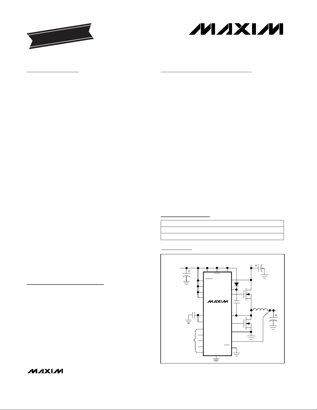
Minimal Operating Circuit
MAX1710/MAX1711
High-Speed, Digitally Adjusted
Step-Down Controllers for Notebook CPUs
2 _______________________________________________________________________________________
ABSOLUTE MAXIMUM RATINGS
Stresses beyond those listed under “Absolute Maximum Ratings” may cause permanent damage to the device. These are stress ratings only, and functional
operation of the device at these or any other conditions beyond those indicated in the operational sections of the specifications is not implied. Exposure to
absolute maximum rating conditions for extended periods may affect device reliability.
V+ to GND..............................................................-0.3V to +30V
V
CC
, VDDto GND.....................................................-0.3V to +6V
PGND to GND.....................................................................±0.3V
SHDN, PGOOD to GND ...........................................-0.3V to +6V
OVP, ILIM, FB, FBS, CC, REF, D0–D4,
GNDS, TON to GND..............................-0.3V to (V
CC
+ 0.3V)
SKIP to GND (Note 1).................................-0.3V to (V
CC
+ 0.3V)
DL to PGND................................................-0.3V to (V
DD
+ 0.3V)
BST to GND............................................................-0.3V to +36V
DH to LX.....................................................-0.3V to (BST + 0.3V)
LX to BST..................................................................-6V to +0.3V
REF Short Circuit to GND...........................................Continuous
Continuous Power Dissipation (T
A
= +70°C)
24-Pin QSOP (derate 9.5mW/°C above +70°C)..........762mW
Operating Temperature Range ...........................-40°C to +85°C
Junction Temperature......................................................+150°C
Storage Temperature Range.............................-65°C to +165°C
Lead Temperature (soldering, 10sec).............................+300°C
V
BATT
= 4.5V to 28V, includes
load regulation error
SHDN = 0, measured at V+ = 28V, VCC= VDD= 0 or 5V
SHDN = 0
V
CC,VDD
SHDN = 0
Battery voltage, V+
Measured at V+
Measured at VDD, FB forced above the regulation point
Measured at VCC, FB forced above the regulation point
Rising edge of SHDN to full I
LIM
(Note 2)
V
BATT
= 24V,
FB = 2V
(Note 2)
FB (MAX1710 only) or FBS
FB-FBS or GNDS-GND = 0 to 25mV
VCC= 4.5V to 5.5V, V
BATT
= 4.5V to 28V
CONDITIONS
µA<1 5
Shutdown Battery Supply
Current
µA<1 5Shutdown Supply Current (VDD)
µA<1 5Shutdown Supply Current (VCC)
µA25 40Quiescent Battery Supply Current
µA<1 5Quiescent Supply Current (VDD)
µA600 950Quiescent Supply Current (VCC)
ns400 500Minimum Off-Time
380 425 470
260 290 320
175 200 225
%
-1 1
DC Output Voltage Accuracy
TON = REF (400kHz)
4.5 5.5
V
2 28
Input Voltage Range
TON = GND (550kHz)
ns
140 160 180
On-Time
ms1.7Soft-Start Ramp Time
µA-1 1GNDS Input Bias Current
µA-0.2 0.2FB Input Bias Current
TON = open (300kHz)
mV3Remote Sense Voltage Error
mV5Line Regulation Error
UNITMIN TYP MAXPARAMETER
Falling edge, hysteresis = 40mV
REF in regulation
I
REF
= 0 to 50µA
VCC= 4.5V to 5.5V, no external REF load
V1.6REF Fault Lockout Voltage
µA10REF Sink Current
V0.01Reference Load Regulation
V1.98 2 2.02Reference Voltage
TON = VCC(200kHz)
Note 1: SKIP may be forced below -0.3V, temporarily exceeding the absolute maximum rating, for the purpose of debugging proto-
type breadboards using the no-fault test mode. Limit the current drawn to -5mA maximum.
ELECTRICAL CHARACTERISTICS
(Circuit of Figure 1, V
BATT
= 15V, VCC= VDD= 5V, SKIP = GND, TA= 0°C to +85°C, unless otherwise noted.)
kΩ130 180 240FB Input Resistance (MAX1711)
DAC codes from 1.3V to 2V
-1.2 1.2
I
LOAD
= 0 to 7A mV9Load Regulation Error
DAC codes from 0.925V
to 1.275V

With respect to unloaded output voltage
MAX1710/MAX1711
High-Speed, Digitally Adjusted
Step-Down Controllers for Notebook CPUs
_______________________________________________________________________________________
3
ELECTRICAL CHARACTERISTICS (continued)
(Circuit of Figure 1, V
BATT
= 15V, VCC= VDD= 5V, SKIP = GND, TA= 0°C to +85°C, unless otherwise noted.)
CONDITIONS UNITMIN TYP MAXPARAMETER
LX to PGND
LX to PGND, ILIM tied to V
CC
From SHDN signal going high
mV
40 50 60
Current-Limit Threshold
(Positive Direction, Adjustable)
mV90 100 110
Current-Limit Threshold
(Positive Direction, Fixed)
ms10 30
Output Undervoltage Protection
Time
%65 70 75
Output Undervoltage Protection
Threshold
LX to PGND, TA= +25°C mV-150 -120 -80
Current-Limit Threshold
(Negative Direction)
R
LIM
= 100kΩ
R
LIM
= 400kΩ 170 200 230
Rising edge, hysteresis = 20mV,
PWM disabled below this level
V4.1 4.4
VCCUndervoltage Lockout
Threshold
BST-LX forced to 5V Ω5DH Gate-Driver On-Resistance
DL, high state Ω5
DL Gate-Driver On-Resistance
(Pull-Up)
DL, low state Ω0.5 1.7
DL Gate-Driver On-Resistance
(Pull-Down)
DH forced to 2.5V, BST-LX forced to 5V A1
DH Gate-Driver Source/Sink
Current
DL forced to 2.5V A3DL Gate-Driver Sink Current
DL forced to 2.5V A1DL Gate-Driver Source Current
FB forced 2% above trip threshold µs1.5
Overvoltage Fault Propagation
Delay
%10.5 12.5 14.5
Overvoltage Trip Threshold
FB forced 2% below PGOOD trip threshold, falling edge µs1.5PGOOD Propagation Delay
LX to PGND mV3
Current-Limit Threshold
(Zero Crossing)
I
SINK
= 1mA V0.4PGOOD Output Low Voltage
High state, forced to 5.5V µA1PGOOD Leakage Current
Hysteresis = 10°C °C150Thermal Shutdown Threshold
V2.21 2.25 2.29
0.76 0.8 0.84
With respect to unloaded output voltage (MAX1710)
With respect to unloaded output voltage (MAX1710)
(MAX1711) V
DL rising
ns
35
Dead Time
DH rising 26
mA
SKIP Input Current Logic
Threshold
To enable no-fault mode, TA= +25°C -1.5 -0.1
%PGOOD Trip Threshold
Measured at FB with respect to unloaded output voltage,
falling edge, hysteresis = 1%
-8 -5 -3
VLogic Input High Voltage
D0–D4, SHDN, SKIP, OVP
2.4
VLogic Input Low Voltage
D0–D4, SHDN, SKIP, OVP
0.8
µALogic Input Current
SHDN, SKIP, OVP
-1 1
µALogic Input Pull-Up Current D0–D4, each forced to GND 3 5 10
(MAX1711)
MAX1710/MAX1711
High-Speed, Digitally Adjusted
Step-Down Controllers for Notebook CPUs
4 _______________________________________________________________________________________
%10 15
V
BATT
= 4.5V to 28V, for all
D/A codes, includes load
regulation error
V
CC,VDD
Battery voltage, V+
Measured at VCC, FB forced above the regulation point
Overvoltage Trip Threshold
(Note 2)
V
BATT
= 24V,
FB = 2V
(Note 2)
With respect to unloaded output voltage (MAX1710) %
CONDITIONS
65 75
Output Undervoltage
Protection Threshold
µA950Quiescent Supply Current (VCC)
ns500Minimum Off-Time
380 470
260 320
175 225
%-1.5 1.5
DC Output Voltage Accuracy
TON = REF (400kHz)
4.5 5.5
V
2 28
Input Voltage Range
TON = GND (550kHz)
ns
140 180
On-Time
TON = open (300kHz)
UNITMIN TYP MAXPARAMETER
VCC= 4.5V to 5.5V, no external REF load V1.98 2.02Reference Voltage
TON = VCC(200kHz)
LX to PGND, ILIM tied to V
CC
mV85 115
Current-Limit Threshold
(Positive Direction, Fixed)
LX to PGND mV
35 65
Current-Limit Threshold
(Positive Direction, Adjustable)
R
LIM
= 100kΩ
R
LIM
= 400kΩ 160 240
Rising edge, hysteresis = 20mV, PWM disabled below
this level
4.1 4.4
VCCUndervoltage Lockout
Threshold
V
D0–D4, SHDN, SKIP, OVP
V2.4Logic Input High Voltage
D0–D4, SHDN, SKIP, OVP
V0.8Logic Input Low Voltage
SHDN, SKIP, OVP
µA-1 1Logic Input Current
D0–D4, each forced to GND µA3 10Logic Input Pull-Up Current
ELECTRICAL CHARACTERISTICS
(Circuit of Figure 1, V
BATT
=15V, V
CC
= VDD= 5V, SKIP = GND, TA= -40°C to +85°C, unless otherwise noted.) (Note 3)
V2.20 2.30
0.75 0.85 V
ELECTRICAL CHARACTERISTICS (continued)
(Circuit of Figure 1, V
BATT
= 15V, VCC= VDD= 5V, SKIP = GND, TA= 0°C to +85°C, unless otherwise noted.)
CONDITIONS
TON logic input high level VVCC- 0.4TON VCCLevel
TON logic input upper-mid-range level V3.15 3.85TON Float Voltage
TON logic input lower-mid-range level V1.65 2.35TON Reference Level
TON logic input low level V0.5TON GND Level
TON only, forced to GND or V
CC
µA-3 3TON Logic Input Current
UNITMIN TYP MAXPARAMETER
With respect to unloaded output voltage (MAX1710)
(MAX1711)
(MAX1711)
%-1.7 1.7
DAC codes from 1.32V to 2V
DAC codes from 0.925V to
1.275V
MAX1710/MAX1711
High-Speed, Digitally Adjusted
Step-Down Controllers for Notebook CPUs
_______________________________________________________________________________________
5
40
60
50
80
70
90
100
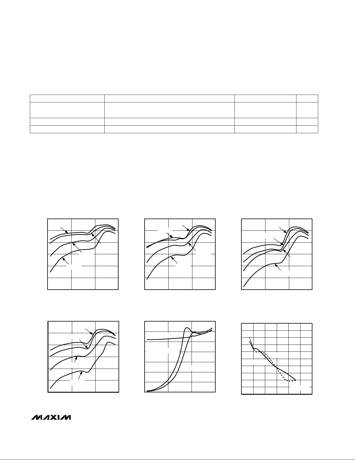
0.01 0.1 1 10
EFFICIENCY vs. LOAD CURRENT
(V
O
= 2.0V, f = 300kHz)
MAX1710-01
LOAD CURRENT (A)
EFFICIENCY (%)
VIN = 4.5V
VIN = 7V
VIN = 15V
VIN = 24V
40
60
50
80
70
90
100
0.01 0.1 1 10
EFFICIENCY vs. LOAD CURRENT
(V
O
= 1.6V, f = 300kHz)
MAX1710-02
LOAD CURRENT (A)
EFFICIENCY (%)
VIN = 4.5V
VIN = 24V
VIN = 7V
VIN = 15V
40
60
50
80
70
90
100
0.01 0.1 1 10
EFFICIENCY vs. LOAD CURRENT
(V
O
= 1.3V, f = 300kHz)
MAX1710-03
LOAD CURRENT (A)
EFFICIENCY (%)
VIN = 4.5V
VIN = 24V
VIN = 15V
VIN = 7V
40
60
50
80
70
90
100
0.01 0.1 1 10
EFFICIENCY vs. LOAD CURRENT
(V
O
= 1.6V, f = 550kHz)
MAX1710-04
LOAD CURRENT (A)
EFFICIENCY (%)
VIN = 4.5V
VIN = 15V
VIN = 7V
VIN = 24V
0
100
50
200
150
300
250
350
0.01 0.1 1 10
FREQUENCY vs. LOAD CURRENT
(V
O
= 1.6V)
MAX1710-05
LOAD CURRENT (A)
FREQUENCY (kHz)
VIN = 15V, PWM MODE
VIN = 4.5V, SKIP MODE
VIN = 15V, SKIP MODE
TON = OPEN
300
306
304
302
308
310
312
314
316
318
320
0 105 15 20 25 30
FREQUENCY vs. INPUT VOLTAGE
(I
O
= 7A)
MAX1710-06
INPUT VOLTAGE (V)
FREQUENCY (kHz)
VO = 2.0V
VO = 1.6V
TON = OPEN
Note 2: On-Time and Off-Time specifications are measured from 50% point to 50% point at the DH pin with LX forced to 0V, BST
forced to 5V, and a 250pF capacitor connected from DH to LX. Actual in-circuit times may differ due to MOSFET switching
speeds.
Note 3: Specifications from -40°C to 0°C are guaranteed but not production tested.
__________________________________________Typical Operating Characteristics
(7A CPU supply circuit of Figure 1, TA= +25°C, unless otherwise noted.)
CONDITIONS
Measured at FB with respect to unloaded output voltage,
falling edge, hysteresis = 1%
%-8.5 -2.5PGOOD Trip Threshold
I
SINK
= 1mA V0.4PGOOD Output Low Voltage
High state, forced to 5.5V µA1PGOOD Leakage Current
UNITMIN TYP MAXPARAMETER
ELECTRICAL CHARACTERISTICS (continued)
(Circuit of Figure 1, V
BATT
=15V, V
CC
= VDD= 5V, SKIP = GND, TA= -40°C to +85°C, unless otherwise noted.) (Note 3)
MAX1710/MAX1711
High-Speed, Digitally Adjusted
Step-Down Controllers for Notebook CPUs
6 _______________________________________________________________________________________
_____________________________Typical Operating Characteristics (continued)
(7A CPU supply circuit of Figure 1, TA= +25°C, unless otherwise noted.)
0
0.2
0.1
0.5
0.4
0.3
0.8
0.7
0.6
0.9
0 105 15 20 25 30
CONTINUOUS TO DISCONTINUOUS
INDUCTOR CURRENT POINT
vs. INPUT VOLTAGE
MAX1710-10
INPUT VOLTAGE (V)
LOAD CURRENT (A)
VO = 2.0V
VO = 1.6V
VO = 1.3V
10.0
10.5
11.0
11.5
12.0
12.5
13.0
13.5
14.0
0 105 15 20 25 30
INDUCTOR CURRENT PEAKS AND
VALLEYS vs. INPUT VOLTAGE
(AT CURRENT-LIMIT POINT)
MAX1710-11
INPUT VOLTAGE (V)
INDUCTOR CURRENT (A)
I
PEAK
I
VALLEY
0
0.2
0.1
0.4
0.3
0.6
0.5
0.7
0 5 15 2510 20 30
NO-LOAD SUPPLY CURRENTS
vs. INPUT VOLTAGE
(SKIP MODE, f = 300kHz)
MAX1710-12
INPUT VOLTAGE (V)
SUPPLY CURRENT (mA)
I
CC
I
BATT
I
DD
0
0.2
0.1
0.4
0.3
0.6
0.5
0.7
0 10 20 305 15 25
NO-LOAD SUPPLY CURRENTS
vs. INPUT VOLTAGE
(SKIP MODE, f = 550kHz)
MAX1710-13
INPUT VOLTAGE (V)
SUPPLY CURRENT (mA)
I
CC
I
BATT
I
DD
0
6
4
2
8
10
12
14
16
18
20
0 105 15 20 25 30
NO-LOAD SUPPLY CURRENTS
vs. INPUT VOLTAGE
(PWM MODE, f = 300kHz)
MAX1710-14
INPUT VOLTAGE (V)
SUPPLY CURRENT (mA)
I
DD
I
BAT
I
CC
0
6
4
2
8
10
12
14
16
18
20
0 105 15 20 25 30
NO-LOAD SUPPLY CURRENTS
vs. INPUT VOLTAGE
(PWM MODE, f = 550kHz)
MAX1710-15
INPUT VOLTAGE (V)
SUPPLY CURRENT (mA)
I
DD
I
BAT
I
CC
285
290
295
300
305
310
315
-60 -20-40 0 20 40 60 80 100
FREQUENCY vs. TEMPERATURE
(V
IN
= 15V, VO = 2.0V)
MAX1710-07
TEMPERATURE (°C)
FREQUENCY (kHz)
IO = 7A
IO = 4A
IO = 1A
TON = OPEN
456
460
458
466
464
462
472
470
468
474
-60 0 20-40 -20 40 60 80 100
ON-TIME vs. TEMPERATURE
MAX1710-08
TEMPERATURE (°C)
ON TIME (ns)
IO = 1A
IO = 4A OR 7A
0
5
10
15
20
25
30
-60 -20-40 0 20 40 60 80 100
CURRENT-LIMIT TRIP POINT
vs. TEMPERATURE
MAX1710-09
TEMPERATURE (°C)
CURRENT TRIP POINT (A)
I
LIM
= 400kΩ
I
LIM
= V
CC
I
LIM
= 100kΩ
10µs/div
LOAD-TRANSIENT RESPONSE
(WITH INTEGRATOR)
VIN = 15V, VO = 1.6V, IO = 0A TO 7A
A = V
OUT
, AC COUPLED, 50mV/div
B = INDUCTOR CURRENT, 5A/div
A
B
MAX1710-16
10µs/div
LOAD-TRANSIENT RESPONSE
(WITH INTEGRATOR)
VIN = 15V, VO = 1.6V, IO = 30mA, TO 7A
A = V
OUT
, AC COUPLED, 50mV/div
B = INDUCTOR CURRENT, 5A/div
A
B
MAX1710-17
MAX1710/MAX1711
High-Speed, Digitally Adjusted
Step-Down Controllers for Notebook CPUs
_______________________________________________________________________________________ 7
_____________________________Typical Operating Characteristics (continued)
(7A CPU supply circuit of Figure 1, TA= +25°C, unless otherwise noted.)
20µs/div
LOAD-TRANSIENT RESPONSE
(WITH INTEGRATOR)
VIN = 4.5V, VO = 2V, IO = 30mA TO 7A
A = V
OUT
, AC COUPLED, 50mV/div
B = INDUCTOR CURRENT, 5A/div
C = DL, 10V/div
A
B
C
MAX1710-19
20µs/div
LOAD-TRANSIENT RESPONSE
(WITH INTEGRATOR)
VIN = 4.5V, VO = 1.3V, IO = 30mA TO 7A
A = V
OUT
, AC COUPLED, 50mV/div
B = INDUCTOR CURRENT, 5A/div
C = DL, 10V/div
A
B
C
MAX1710-20
500µs/div
START-UP WAVEFORM
A = SHDN
B = V
OUT
, 0.5V/div
C = INDUCTOR CURRENT, 5A/div
A
B
C
MAX1710-21
10µs/div
LOAD-TRANSIENT RESPONSE
(WITHOUT INTEGRATOR)
VIN = 15V, VO = 1.6V, IO = 30mA TO 7A
A = V
OUT
, AC COUPLED, 50mV/div
B = INDUCTOR CURRENT, 5A/div
A
B
MAX1710-18

MAX1710/MAX1711
High-Speed, Digitally Adjusted
Step-Down Controllers for Notebook CPUs
8 _______________________________________________________________________________________
50µs/div
OUTPUT OVERLOAD WAVEFORM
V
OUT
= 1.6V
A = V
IN
, AC COUPLED, 2V/div
B = V
OUT
, 0.5V/div
C = INDUCTOR CURRENT, 5A/div
A
B
C
MAX1710-22
5µs/div
LOAD-TRANSIENT RESPONSE
L = 0.7µH, V
OUT
= 1.6V, VIN = 15V, C
OUT
= 47µF (x4), f = 550kHz
A = V
OUT
, AC COUPLED, 100mV/div
B = INDUCTOR CURRENT, 5A/div
C = DL, 5V/div
A
B
C
MAX1710-23
CERAMIC C
OUT
5µs/div
SHUTDOWN WAVEFORM
VIN = 15V, V0 = 1.6V, I0 = 7A
A = V
OUT
, 0.5V/div
B = INDUCTOR CURRENT, 5A/div
C = SHDN, 2V/div
D = DL, 5V/div
A
B
C
D
MAX1710-24
_____________________________Typical Operating Characteristics (continued)
(7A CPU supply circuit of Figure 1, TA= +25°C, unless otherwise noted.)
Pin Description
NAME FUNCTION
5 CC
Integrator Capacitor Connection. Connect a 100pF to 1000pF (470pF typical) capacitor to GND to set the
integration time constant.
PIN
4 FBS
Feedback Remote-Sense Input, normally connected to V
OUT
directly at the load. FBS internally connects to
the integrator that fine-tunes the DC output voltage. Tie FBS to VCCto disable all three integrator amplifiers.
Tie FBS to FB (or disable the integrators) when externally adjusting the output voltage with a resistor-divider.
3 FB
Fast Feedback Input, normally connected to V
OUT
. FB is connected to the bulk output filter capacitors local-
ly at the power supply. An external resistor-divider can optionally set the output voltage.
8 TON
On-Time Selection Control Input. This is a four-level input that sets the K factor to determine DH on-time.
GND = 550kHz, REF = 400kHz, open = 300kHz, V
CC
= 200kHz.
7 V
CC
Analog Supply Voltage Input for PWM Core, 4.5V to 5.5V. Bypass VCCto GND with a 0.1µF minimum
capacitor.
6 ILIM
Current-Limit Threshold Adjustment. Connects to an external resistor to GND. The LX-PGND current-limit
threshold defaults to +100mV if ILIM is tied to VCC. The current-limit threshold is 1/10 of the voltage forced at
ILIM. In adjustable mode the threshold is V
TH
= R
LIM
· 5µA/10.
1 CC
Battery Voltage Sense Connection. V+ is used only for PWM one-shot timing. DH on-time is inversely proportional to V+ input voltage over a range of 2V to 28V.
9 REF
2.0V Reference Output. Bypass REF to GND with a 0.22µF minimum capacitor. REF can source 50µA for
external loads. Loading REF degrades FB accuracy according to the REF load-regulation error
(see
Electrical Characteristics
).
2
SHDN
Shutdown Control Input, active low. SHDN cannot withstand the battery voltage. In shutdown mode, DL is
forced to V
DD
in order to enforce overvoltage protection, even when powered down (unless OVP is high).
MAX1710/MAX1711
High-Speed, Digitally Adjusted
Step-Down Controllers for Notebook CPUs
_______________________________________________________________________________________ 9
Standard Application Circuit
The standard application circuit (Figure 1) generates a
low-voltage, high-power rail for supplying up to 7A to the
core CPU VCCin a notebook computer. This DC-DC
converter steps down a battery or AC adapter voltage to
sub-2V levels with high efficiency and accuracy, and
represents a good compromise between size, efficiency,
and cost.
See the MAX1710 EV kit manual for a list of components
and suppliers.
Detailed Description
The MAX1710/MAX1711 buck controllers are targeted
for low-voltage, high-current CPU power supplies for
notebook computers. CPU cores typically exhibit 0 to
10A or greater load steps when the clock is throttled.
The proprietary QUICK-PWM pulse-width modulator in
the MAX1710/MAX1711 is specifically designed for handling these fast load steps while maintaining a relatively
constant operating frequency and inductor operating
point over a wide range of input voltages. The QUICKPWM architecture circumvents the poor load-transient
timing problems of fixed-frequency current-mode PWMs
Pin Description (continued)
NAME FUNCTION
16
(MAX1711)
D4 DAC Code Input, MSB, 5µA internal pull-up to VCC(Tables 1 and 2).
PIN
13 DL Low-Side Gate-Driver Output, swings 0 to VDD.
12 PGOOD Open-Drain Power-Good Output.
11 GNDS
Ground Remote-Sense Input, normally connected to ground directly at the load. GNDS internally connects to the integrator that fine-tunes the ground offset voltage.
10 GND Analog Ground
14 PGND Power Ground. Also used as the inverting input for the current-limit comparator.
15 V
DD
Supply Voltage Input for the DL gate driver, 4.5V to 5.5V
17 D3 DAC Code Input. 5µA internal pull-up to VCC.
16
(MAX1710)
OVP
Overvoltage-Protection Disable Control Input (Table 3). GND = normal operation and overvoltage
protection active, V
CC
= overvoltage protection disabled.
22 BST
Boost Flying-Capacitor Connection. An optional resistor in series with BST allows the DH pull-up
current to be adjusted (Figure 5). This technique of slowing the LX rise time can be used to prevent
accidental turn-on of the low-side MOSFET due to excessive gate-drain capacitance.
21
SKIP
Low-Noise-Mode Selection Control Input. Low-noise forced-PWM mode causes inductor current
recirculation at light loads and suppresses pulse-skipping operation. Normal operation prevents
current recirculation. SKIP can also be used to disable both overvoltage and undervoltage protection
circuits and clear the fault latch (Figure 6). GND = normal operation, V
CC
= low-noise mode. Do not
leave
SKIP floating.
20 D0 DAC Code Input LSB. 5µA internal pull-up.
19 D1 DAC Code Input. 5µA internal pull-up.
18 D2 DAC Code Input. 5µA internal pull-up.
24 DH High-Side Gate-Driver Output. Swings LX to BST.
23 LX
Inductor Connection. LX serves as the lower supply rail for the DH high-side gate driver. Also used
for the noninverting input to the current-limit comparator as well as the skip-mode zero-crossing comparator.
 Loading...