

Page 1
EMF32 / UMF32N
Transistors
Power management (dual transistors)
EMF32 / UMF32N
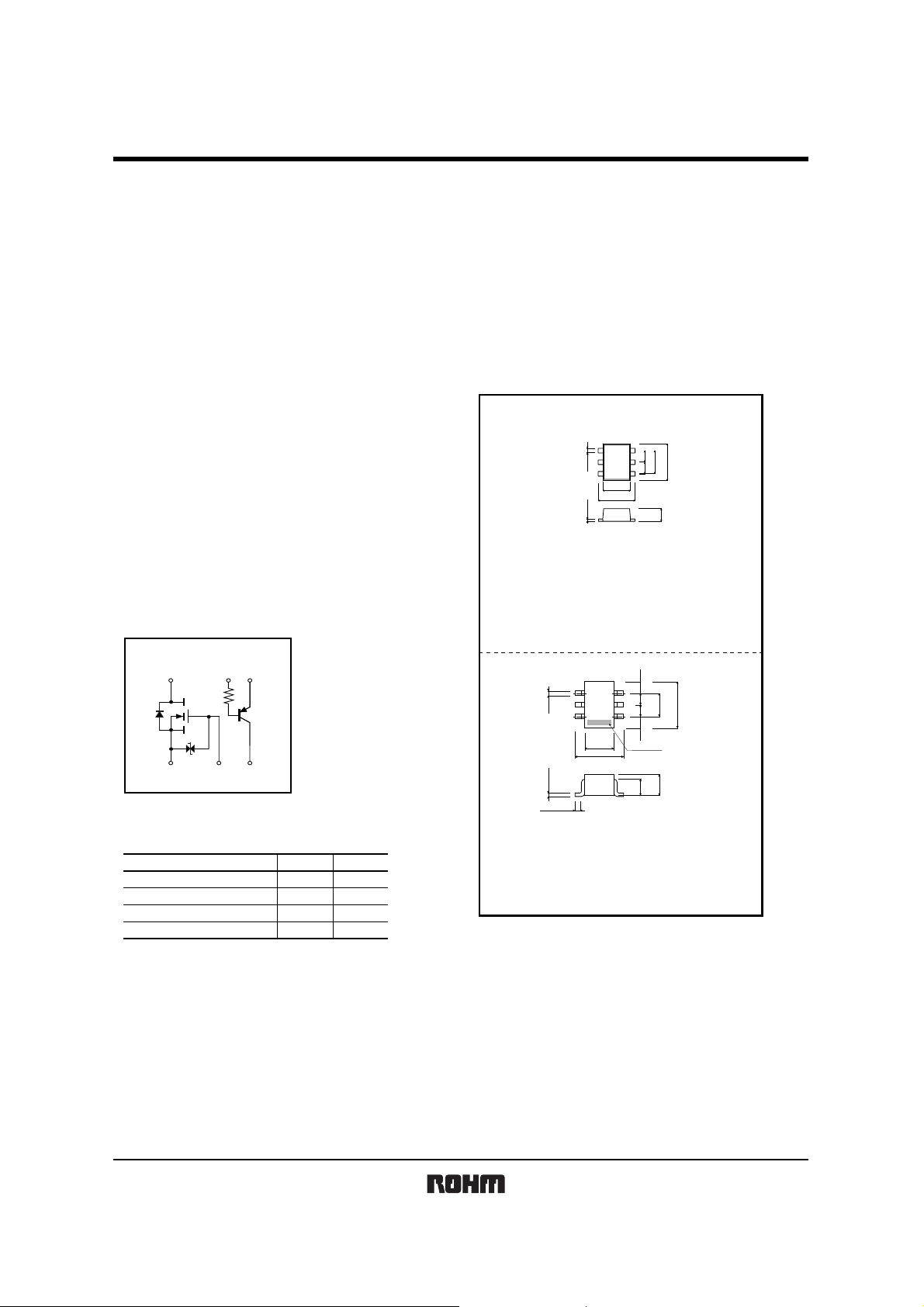
DTA143T and 2SK3019 are housed independently in a EMT6 package.
zApplica tion
Power management circuit
zFeatures
1) Power switching circuit in a single package.
2) Mounting cost and area can be cut in half.
zStructure
Silicon epitaxial planar transistor
zEquivalent circuit s
zExternal dimensions (Unit : mm)
(3)
ROHM : EMT6
Abbreviated symbol : F32
0.22
0.13
(4)
(6)
0.5
1.0
(2)(5)
0.5
(1)
1.2
1.6
0.5
Each lead has
same dimensions
1.6
(1)(2)(3)
Tr2
(4) (5) (6)
Tr1
zPackaging specifications
Type
Package
Marking
Code
Basic ordering unit (pieces)
EMF32
EMT6
F32
T2R
8000
UMF32
UMT6
F32
TR
3000
)
)
3
4
(
)
5
(
0.2
0.15
0.1Min.
ROHM : UMT6
)
6
(
1.25
2.1
0.65
(
)
2
(
1.3
)
1
(
0.65
1pin mark
0.9
0.7
Each lead has
2.0
same dimensions
Abbreviated symbol : F32
1/4
Page 2
Transistors
zAbsolute maximum ratings (Ta=25°C)
Tr1
Parameter Symbol
CBO
Collector-base voltage
Collector-emitter voltage
Emitter-base voltage
Collector current
Power dissipation
Junction temperature
Range of storage temperature
∗1 120mW per element must not be exceeded. Each terminal mounted on a recommended land.
V
V
CEO
V
EBO
I
P
Tj
Tstg
C
C
Tr2
Parameter
Drain-source voltage
Gate-source voltage
Drain current
Reverse drain
current
Continuous
Pulsed
Continuous
Pulsed
Total power dissipation
Channel temperature
Range of storage temperature
∗1 PW≤10ms Duty cycle≤50%
∗2 120mW per element must not be exceeded. Each terminal mounted on a recommended land.
Symbol
DSS
V
V
GSS
I
D
DP
I
I
DR
I
DRP
P
D
Tch
Tstg
zElectrical characteristics (Ta=25°C)
Tr1
Parameter Symbol
Collector-base breakdown voltage
Collector-emitter breakdown voltage
Emitter-base breakdown voltage
Collector cutoff current
Emitter cutoff current
Collector-emitter saturation voltage
DC current transfer ratio
Input resistance
Transition frequency
∗ Transition frequency of the device
BV
BV
BV
V
Tr2
Parameter
Gate-source leakage
Drain-source breakdown voltage
Zero gate voltage drain current
Gate-threshold voltage
Static drain-source
on-state resistance
Forward transfer admittance
Input capacitance
Output capacitance
Reverce transfer capacitance
Turn-on delay time
Rise time
Turn-off delay time
Fall time
CBO
CEO
EBO
I
CBO
I
EBO
CE(sat)
h
FE
R
1
f
T
Symbol
I
GSS
(BR)DSS
V
DSS
I
V
GS(th)
DS(on)
R
|Y
iss
C
C
oss
rss
C
t
d(on)
r
t
t
d(off)
t
fs
f
Limits
−50
−50
−5
−100
150(TOTAL)
150
−55 to +150
Limits
30
±20
100
200 mA
Unit
V
V
V
mA
mW
°C
°C
Unit
V
V
mA
∗1
∗1
100 mA
∗1
200
150(TOTAL)
150
−55 to +150
Min.
−50
−50
−5
−
−
−
100
3.29
−
Min. Typ. Max. Unit Conditions
|
mA
∗2
mW
°C
°C
Typ. Max. Unit Conditions
−
−
VI
−
−
−
−
−
250
4.7
250
−−
30
−−
0.8
−
−
20
13
−
−
−
15
−
35
−
80
−
80
−
V
−
V
−
µA
−0.5
µA
−0.5
V
−0.3
−
600
kΩ
6.11 −
MHz
−
±1 µA
−−
1.0 µA
1.5
−
58Ω
713Ω
−−ms V
−
9
− pF
4
− pF
− ns
−
− ns
− ns
C
=
−50µA
I
C
=
−1mA
I
E
=
−50µA
V
CB
=
−50V
V
EB
=
−4V
C/IB
=
−5mA/ −0.25mA
I
C
=
−1mA, V
CE
I
V
CE
=
V
VV
pF
ns
=
−
10V, IE=5mA, f=100MHz
VGS=±20V, VDS=0V
ID=10µA, VGS=0V
VDS=30V, VGS=0V
DS
=3V, ID=100µA
ID=10mA, VGS=4V
D
=1mA, VGS=2.5V
I
DS
=3V, ID=10mA
DS
=5V, VGS=0V, f=1MHz
V
D
=10mA, VDD 5V,
I
GS
=5V, RL=500Ω,
V
GS
=10Ω
R
EMF32 / UMF32N
−5V
∗
2/4
Page 3

Transistors
zElectrical characteristic curves
Tr1
1k
500
FE
200
100
50
20
10
DC CURRENT GAIN : h
Ta=100°C
25°C
−40°C
5
2
1
−100µ−1m −10m−200µ−2m −20m−500µ−5m −50m −100m
COLLECTOR CURRENT : I
Fig.1
DC current gain vs. collector
current
Tr2
0.15
(A)
D
0.1
0.05
DRAIN CURRENT : I
4V
0
012345
DRAIN-SOURCE VOLTAGE : VDS (V)
3V
3.5V
2.5V
2V
VGS=1.5V
V
CE
=−
C
(A)
Ta=25°C
Pulsed
EMF32 / UMF32N
−1
5V
(V)
−500m
CE(sat)
−200m
−100m
−50m
−20m
−10m
−5m
−2m
−1m
−100µ−1m
COLLECTOR SATURATION VOLTAGE : V
Ta=100°C
25°C
−40°C
−200µ−2m
−500µ−5m
COLLECTOR CURRENT : I
−10m
−20m
C
lC/lB=20
(A)
Fig.2 Collector-emitter saturation
voltage vs. collector current
200m
VDS
=3V
100m
Pulsed
50m
(A)
D
20m
10m
5m
2m
1m
0.5m
DRAIN CURRENT : I
0.2m
0.1m
04
1
GATE-SOURCE VOLTAGE : VGS (V)
Ta=125°C
75°C
25°C
−25°C
2
3
−50m−100m
2
(V)
GS(th)
1.5
1
0.5
GATE THRESHOLD VOLTAGE : V
0
−50 0
−25 25 50 75 100 125 150
CHANNEL TEMPERATURE : Tch (°C)
V
DS
D
=0.1mA
I
Pulsed
=3V
Fig.3 Typical output characteristics
50
(Ω)
DS(on)
STATIC DRAIN-SOURCE
ON-STATE RESISTANCE : R
Ta=125°C
20
10
0.5
5
2
1
0.001
75°C
25°C
−25°C
0.002 0.005 0.01 0.02 0.05 0.1 0.2 0.5
DRAIN CURRENT : ID (A)
Fig.6 Static drain-source on-state
resistance vs. drain current ( Ι )
V
GS
Pulsed
=4V
Fig.4 Typical transfer characteristics
50
Ta=125°C
(Ω)
20
DS(on)
10
5
2
1
STATIC DRAIN-SOURCE
ON-STATE RESISTANCE : R
0.5
0.001
75°C
25°C
−25°C
0.002 0.005 0.01 0.02 0.05 0.1 0.2 0.5
DRAIN CURRENT : ID (A)
V
GS
Pulsed
Fig.7 Static drain-source on-state
resistance vs. drain current ( ΙΙ )
=2.5V
Fig.5 Gate threshold voltage vs.
channel temperature
15
(Ω)
DS(on)
10
5
STATIC DRAIN-SOURCE
ON-STATE RESISTANCE : R
0
0 5 10 15 20
GATE-SOURCE VOLTAGE : VGS (V)
ID=0.1A
ID=0.05A
Fig.8 Static drain-source on-state
resistance vs. gate-source
voltage
Ta=25°C
Pulsed
3/4
Page 4

Transistors
9
8
(Ω)
7
DS(on)
STATIC DRAIN-SOURCE
ON-STATE RESISTANCE : R
ID=100mA
6
5
4
3
2
1
0
−50 0 25 150
−25 50 75 100 125
CHANNEL TEMPERATURE : Tch (°C)
ID=50mA
VGS=4V
Pulsed
0.5
0.2
Ta=−25°C
0.1
0.05
0.02
0.01
0.005
FORWARD TRANSFER
ADMITTANCE : |Yfs| (S)
0.002
0.001
0.0001
25°C
75°C
125°C
0.0002 0.0005 0.001 0.002 0.005 0.01 0.02 0.05
DRAIN CURRENT : ID (A)
V
DS
=3V
Pulsed
0.1 0.2 0.5
EMF32 / UMF32N
200m
(A)
100m
DR
50m
20m
10m
5m
2m
1m
0.5m
REVERSE DRAIN CURRENT : I
0.2m
0.1m
SOURCE-DRAIN VOLTAGE : VSD (V)
Ta=125°C
75°C
25°C
−25°C
10.50
V
GS
Pulsed
=0V
1.5
Fig.9 Static drain-source on-state
resistance vs. channel temperature
200m
(A)
100m
DR
50m
20m
10m
V
GS
=4V
5m
2m
1m
0.5m
REVERSE DRAIN CURRENT : I
0.2m
0.1m
SOURCE-DRAIN VOLTAGE : VSD (V)
0V
Fig.12 Reverse drain current vs.
source-drain voltage ( ΙΙ )
Ta=25°C
Pulsed
10.50
Fig.10 Forward transfer admittance vs.
drain current
50
20
10
5
2
CAPACITANCE : C (pF)
1
0.5
0.1
1.5
0.2 0.5 1 2 5 10 20 50
DRAIN-SOURCE VOLTAGE : VDS (V)
Fig.13 Typical capacitance vs.
drain-source voltage
Ta=25°C
f=1MH
VGS=0V
C
iss
C
oss
C
rss
Z
SWITHING TIME : t (ns)
Fig.11 Reverse drain current vs.
source-drain voltage ( Ι )
1000
500
200
100
50
20
10
5
2
0.1
t
f
t
d(off)
t
r
t
d(on)
0.2 0.5 1 2 5 10 20 50
DRAIN CURRENT : ID (mA)
Fig.14 Switching characteristics
Ta
=25°C
DD=5V
V
GS=5V
V
RG=10Ω
Pulsed
100
4/4
Page 5

Appendix
No technical content pages of this document may be reproduced in any form or transmitted by any
means without prior permission of ROHM CO.,LTD.
The contents described herein are subject to change without notice. The specifications for the
product described in this document are for reference only. Upon actual use, therefore, please request
that specifications to be separately delivered.
Application circuit diagrams and circuit constants contained herein are shown as examples of standard
use and operation. Please pay careful attention to the peripheral conditions when designing circuits
and deciding upon circuit constants in the set.
Any data, including, but not limited to application circuit diagrams information, described herein
are intended only as illustrations of such devices and not as the specifications for such devices. ROHM
CO.,LTD. disclaims any warranty that any use of such devices shall be free from infringement of any
third party's intellectual property rights or other proprietary rights, and further, assumes no liability of
whatsoever nature in the event of any such infringement, or arising from or connected with or related
to the use of such devices.
Upon the sale of any such devices, other than for buyer's right to use such devices itself, resell or
otherwise dispose of the same, no express or implied right or license to practice or commercially
exploit any intellectual property rights or other proprietary rights owned or controlled by
ROHM CO., LTD. is granted to any such buyer.
Products listed in this document are no antiradiation design.
Notes
The products listed in this document are designed to be used with ordinary electronic equipment or devices
(such as audio visual equipment, office-automation equipment, communications devices, electrical
appliances and electronic toys).
Should you intend to use these products with equipment or devices which require an extremely high level of
reliability and the malfunction of with would directly endanger human life (such as medical instruments,
transportation equipment, aerospace machinery, nuclear-reactor controllers, fuel controllers and other
safety devices), please be sure to consult with our sales representative in advance.
About Export Control Order in Japan
Products described herein are the objects of controlled goods in Annex 1 (Item 16) of Export Trade Control
Order in Japan.
In case of export from Japan, please confirm if it applies to "objective" criteria or an "informed" (by MITI clause)
on the basis of "catch all controls for Non-Proliferation of Weapons of Mass Destruction.
Appendix1-Rev1.1
Page 6

 Loading...