

Page 1

INTEGRATED CIRCUITS
DATA SH EET
UAA3202M
Frequency Shift Keying (FSK)
receiver
Preliminary specification
File under Integrated Circuits, IC01
1997 Aug 12
Page 2

Philips Semiconductors Preliminary specification
Frequency Shift Keying (FSK) receiver UAA3202M
FEATURES
• Low cost single-chip FSK receiver
• Superheterodyne architecture with high integration level
• Few external low cost components
• Wide supply voltage range
• Low power consumption
• Wide frequency range, 150 to 450 MHz
• High sensitivity
• IF band determined by application
• High selectivity
• Very low spurious radiation, −60 dBm
(meets FTZ 17TR2100)
• Automotive temperature range
• Power-down mode
• SSOP20 package.
Applications
• Keyless entry systems
• Car alarm systems
• Remote control systems
• Security systems
• Telemetry systems
• Wireless data transmission
• Domestic appliances.
GENERAL DESCRIPTION
The UAA3202M is a fully integrated single-chip receiver,
primarily intended for use in VHF and UHF systems
employing direct Frequency Shift Keying (FSK)
modulation. The UAA3202M incorporates a SAW
stabilized local oscillator, balanced mixer, IF amplifier,
limiter, Received Signal Strength Indicator (RSSI), RSSI
comparator, FSK demodulator, data filter and data slicer.
The device features a power-down mode in order to
minimize the average receiver supply current.
QUICK REFERENCE DATA
SYMBOL PARAMETER CONDITIONS MIN. TYP. MAX. UNIT
V
CC
I
CC
P
sens
supply voltage 3.5 − 6V
supply current for
operating mode on V
operating mode off V
sensitivity fi= 433.92 MHz;
=0V; R2= 560 Ω 2.0 3.4 4.7 mA
PWD
PWD=VCC
− 330µA
−−−94 dBm
f
= 250 Hz square wave;
mod
∆f=±25 kHz; BER ≤ 3%
T
amb
operating ambient temperature −40 − +85 °C
ORDERING INFORMATION
TYPE
NUMBER
NAME DESCRIPTION VERSION
UAA3202M SSOP20
plastic shrink small outline package; 20 leads; body width 5.3 mm
PACKAGE
SOT339-1
1997 Aug 12 2
Page 3
Philips Semiconductors Preliminary specification
Frequency Shift Keying (FSK) receiver UAA3202M
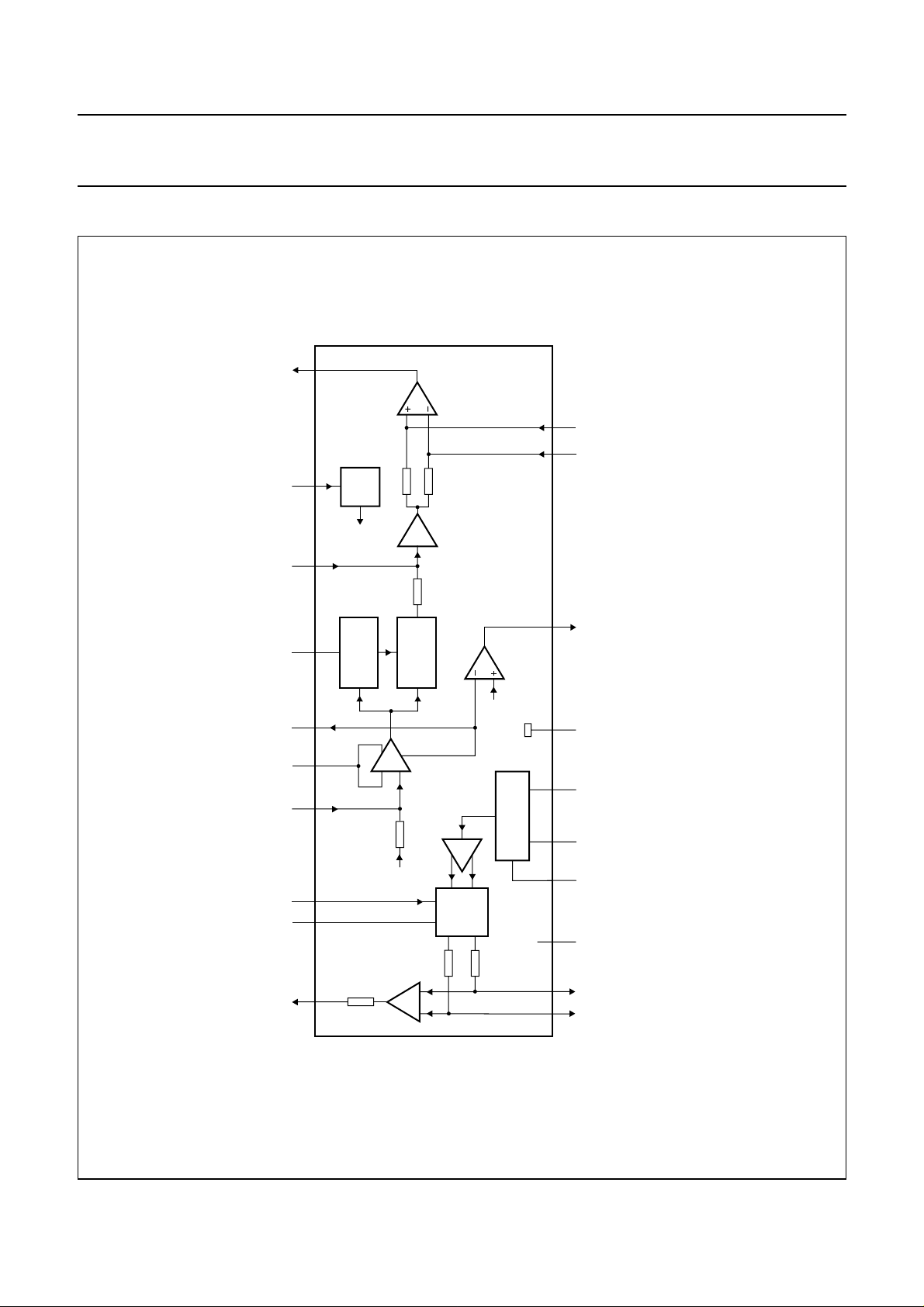
BLOCK DIAGRAM
MHA797
150 kΩ
BIAS
ref
V
150 kΩ
BUFFER
UAA3202M
EM MXIN LIN RSSI DMODLFB CPC PWD DATA
V
FA
30 kΩ
COMP CPB CPA
SHIFT
PHASE
PHASE
DETECTOR
ref
V
RSSI
EE
V
Fig.1 Block diagram.
EO
LIMITER
AMPLIFIER
50 kΩ
CC
V
MIXER
IF
1.4 kΩ
20 19 18 17 16 15 14 13 12 11
AMP
1.5 kΩ
1.5 kΩ
OSCILLATOR
OSC OSE V
CC
12 3 4 5 6 7 8 9 10
MON MOP V
handbook, full pagewidth
1997 Aug 12 3
Page 4
Philips Semiconductors Preliminary specification
Frequency Shift Keying (FSK) receiver UAA3202M
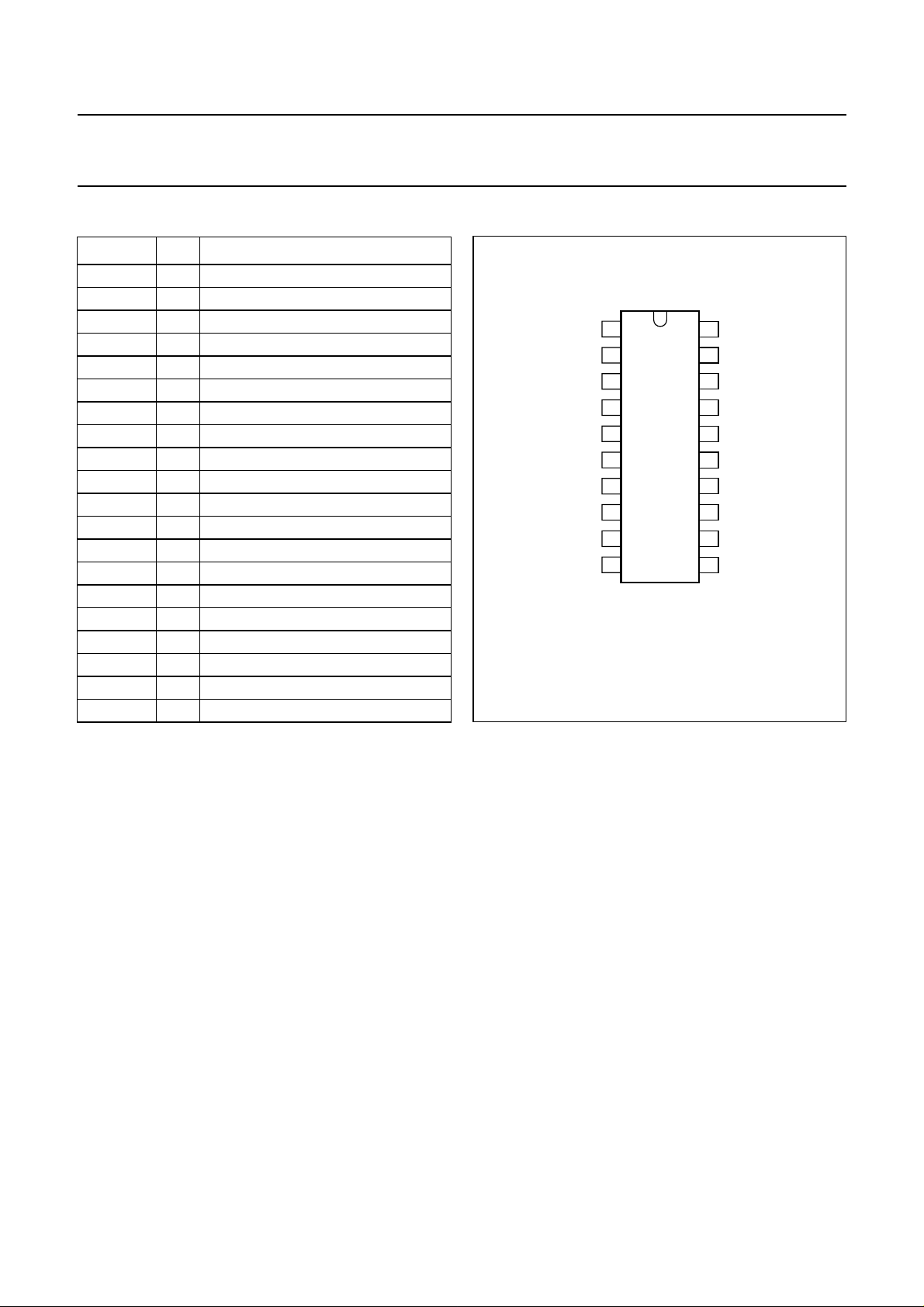
PINNING
SYMBOL PIN DESCRIPTION
MON 1 negative mixer output
MOP 2 positive mixer output
V
CC
3 positive supply voltage
OSC 4 oscillator collector
OSE 5 oscillator emitter
V
EO
V
EE
6 negative supply voltage for oscillator
7 negative supply voltage
COMP 8 RSSI comparator output
CPB 9 comparator input B
CPA 10 comparator input A
DATA 11 data output
PWD 12 power-down control input
CPC 13 comparator input C
DMOD 14 demodulator frequency adjustment
RSSI 15 RSSI current output
LFB 16 limiter feedback
LIN 17 limiter input
MXIN 18 mixer input
V
EM
19 negative supply voltage for mixer
FA 20 IF amplifier output
handbook, halfpage
MON
1
MOP
2
V
3
CC
OSC
4
OSE
5
EO
EE
UAA3202M
6
7
8
9
10
MHA796
V
V
COMP
CPB
CPA
Fig.2 Pin configuration.
20
19
18
17
16
15
14
13
12
11
FA
V
EM
MXIN
LIN
LFB
RSSI
DMOD
CPC
PWD
DATA
1997 Aug 12 4
Page 5

Philips Semiconductors Preliminary specification
Frequency Shift Keying (FSK) receiver UAA3202M
FUNCTIONAL DESCRIPTION
The device is based on the superheterodyne architecture
incorporating a mixer, local oscillator, IF amplifier, limiter,
RSSI, RSSI comparator, FSK demodulator, data filter,
data slicer and power-down circuitry. The device employs
a low IF frequency of typically 1 MHz in order to allow IF
filtering by means of external low cost R, L and C
components. If image rejection is required it can be
achieved by applying a matching external front-end SAW
filter. The device provides a wide IF range of 300 kHz in
order to allow the use of a SAW stabilized oscillator.
The on-chip local oscillator provides the injection signal for
the mixer. Tuning of the on-chip local oscillator is not
necessary. The oscillator frequency is determined by an
external 1-port SAW resonator. The RF input signal is fed
to the mixer and down converted to the IF frequency. After
amplification and filtering the RF signal is applied to a
limiter. The IF filter order and characteristics are
determined by the external low cost R, L and C
components. The limiter amplifier provides a RSSI signal
which can be routed to an on-chip RSSI level comparator
in order to derive a field strength indication for external
use. The limited IF signal is fed to the FSK demodulator.
The demodulator centre frequency is determined by an
external capacitor. No alignment is necessary for the FSK
demodulator. After filtering the demodulated data signal is
fed to a data slicer and is made available at the data
output. The data filter characteristics are determined by
external capacitors. The data slicer employs an adaptive
slice reference in order to track frequency offsets.
The device is switched from power-down to operating
mode and vice versa by means of a control input.
Extremely low supply current is drawn when the device is
in power-down mode. Measures are taken to allow fast
receiver settling when the device is switched from
power-down to operating mode.
Mixer
Post mixer amplifier
The Post Mixer Amplifier (PMA) is a differential input,
single-ended output amplifier. It separates the first and
second IF filters from each other. Amplifier gain is provided
in order to reduce the influence of the limiter noise figure
on the total noise figure.
Limiter
The limiter is a single-ended input multiple stage amplifier
with high total gain. Amplifier stability is achieved by
means of an external DC feedback capacitor, which is also
used to determine the lower limiter cut-off frequency.
An RSSI signal proportional to the limiter input signal is
provided.
IF filters
IF filtering with high selectivity is realized by means of
external low cost R, L and C components. The first IF filter
is located directly following the mixer output. An external
L/C network assembles a band-pass with low sensitivity in
order to meet the bandwidth of an elliptic low-pass filter
external to the device and is located in front of the limiter.
The filter source impedance is determined by the drive
impedance of the IF amplifier. In order to improve the IF
filter selectivity below the pass-band a high-pass
characteristic is added by means of a DC blocking
capacitor in front of the limiter input and by means of the
limiter DC feedback capacitor.
RSSI
The RSSI signal is a current proportional to the limiter input
level (RF input power). By means of an external resistor
the resulting RSSI voltage level is set in order to fit the
application. The RSSI voltage is available to external
circuits and is fed to the input of the RSSI level
comparator. For RSSI filtering an external capacitor is
connected.
The mixer is a single balanced emitter coupled mixer with
internal biasing. Matching of the RF source impedance to
the mixer input requires an external matching network.
Oscillator
The oscillator consists of an on-chip transistor in common
base configuration. An external tank and SAW resonator
determines the oscillator frequency. Oscillator alignment is
not necessary. Oscillator bias is controlled by an external
resistor.
1997 Aug 12 5
RSSI level comparator
The RSSI level comparator compares the RSSI level with
a fixed and independent internal reference voltage. If the
RSSI level exceeds the internal reference voltage a logic
HIGH signal is generated. The level comparator provides
some hysteresis in order to avoid spurious oscillation.
The output of the level comparator is designed as an
open-collector with internal pull-up.
Page 6

Philips Semiconductors Preliminary specification
Frequency Shift Keying (FSK) receiver UAA3202M
FSK demodulator
The limited IF signal is converted into baseband data by
means of a quadrature FM demodulator consisting of an
all-pass filter and a mixer stage. No alignment of the
demodulator is necessary. The demodulator centre
frequency is set by a capacitor external to the device.
The demodulator provides a large audio bandwidth in
order to allow high data rate applications.
The demodulator can detect a small IF frequency deviation
even if a relatively large IF frequency offset is
encountered.
Data filters
After demodulation a two-stage data filtering circuit is
provided in order to suppress unwanted frequency
components. Two R/C low-pass filters with on-chip
resistors are provided which are separated by a buffer
stage.
Data slicer
Data detection is provided by means of a level comparator
with adaptive slice reference. After the first data filter stage
the pre-filtered data is split into two parts. One part passes
the second data filter stage and is fed to the positive
comparator input.
The other path is fed to an integration circuit with a large
time constant in order to derive the average value
(DC component) as an adaptive slice reference which is
presented to the negative comparator input. The adaptive
reference enables the received data over a large range of
demodulator frequency offsets to be detected.
The integration circuit consists of a simple R/C low-pass
filter with on-chip resistor. The level comparator output is
designed as an open-collector with internal pull-up.
Power-down circuitry
The device provides a power-down mode. While in
power-down mode the device disables the majority of the
internal circuits and consumes extremely low current.
Measures are taken to allow fast receiver settling when
normal operation is resumed. Thus circuits with large time
constants are only powered down partly or provide a high
impedance during power-down in order to avoid the
discharge of external capacitors as much as possible.
Power-down mode is entered when the control input is
active HIGH. The control input provides an internal pull-up
resistor of high impedance.
LIMITING VALUES
In accordance with the Absolute Maximum Rating System (IEC 134).
SYMBOL PARAMETER CONDITIONS MIN. MAX. UNIT
V
CC
T
amb
T
stg
V
esd
supply voltage −0.3 +8.0 V
operating ambient temperature −40 +85 °C
storage temperature −55 +125 °C
electrostatic handling note 1
pins 4 and 5 −2000 +1500 V
pins 18 and 19 −1500 +2000 V
all other pins −2000 +2000 V
Note
1. Human body model: equivalent to discharging a 100 pF capacitor through a 1.5 kΩ series resistor.
THERMAL CHARACTERISTICS
SYMBOL PARAMETER VALUE UNIT
R
th j-a
thermal resistance from junction to ambient in free air 125 K/W
1997 Aug 12 6
Page 7

Philips Semiconductors Preliminary specification
Frequency Shift Keying (FSK) receiver UAA3202M
DC CHARACTERISTICS
V
= 3.5 V; T
CC
SYMBOL PARAMETER CONDITIONS MIN. TYP. MAX. UNIT
Supplies
V
CC
I
CC
V
PWD(on)
V
PWD(off)
I
PWD(on)
I
PWD(off)
Oscillator
V
OSC(DC)
Mixer
V
MXIN(DC)
V
MOP(DC)
V
MON(DC)
Post mixer amplifier
V
FA(DC)
Limiter
V
LIN(DC)
V
LFB(DC)
V
RSSI(DC)
Demodulator
V
DMOD(DC)
Data slicer
V
CPC(DC)
V
CPA(DC)
V
CPB(DC)
V
OH(DAT)
V
OL(DAT)
RSSI comparator
V
OH(RSSI)
V
OL(RSSI)
=25°C; for application diagram seeFig.11; unless otherwise specified.
amb
supply voltage 3.5 − 6V
supply current for note 1
operating mode on V
PWD
=0V;
2.0 3.4 4.7 mA
R2= 560 Ω
operating mode off V
PWD=VCC
− 330µA
PWD voltage for operating mode ON 0 − 300 mV
PWD voltage for operating mode OFF VCC− 0.3 − V
PWD current for operating mode ON V
PWD current for operating mode OFF V
=0V −30 −10 −3 µA
PWD
PWD=VCC
− 13µA
CC
V
DC operating point pin 4 3.28 3.34 3.40 V
DC operating point pin 18 0.68 0.78 0.88 V
DC operating point pin 2 2.78 2.98 3.18 V
DC operating point pin 1 2.78 2.98 3.18 V
DC operating point pin 20 2.14 2.27 2.40 V
DC operating point pin 17 3.45 3.49 3.50 V
DC operating point pin 16 2.76 2.81 2.86 V
DC operating point pin 15 2.21 2.36 2.51 V
DC operating point pin 14 1.63 1.83 2.03 V
DC operating point pin 13 note 2 1.43 1.93 2.43 V
DC operating point pin 10 note 2 1.43 1.93 2.43 V
DC operating point pin 9 note 2 1.43 1.93 2.43 V
HIGH-level data output voltage I
LOW-level data output voltage I
HIGH-level comparator output voltage I
LOW-level comparator output voltage I
= −10 µAVCC− 0.5 − V
DATA
= 200 µA0 − 0.6 V
DATA
= −10 µAVCC− 0.5 − V
RSSI
= 200 µA0 − 0.6 V
RSSI
CC
CC
V
V
Notes
1. The given values are valid for the whole temperature range from T
2. Tune RF input frequency until IF = 1 MHz.
1997 Aug 12 7
= −40 to +85 °C.
amb
Page 8

Philips Semiconductors Preliminary specification
Frequency Shift Keying (FSK) receiver UAA3202M
AC CHARACTERISTICS
V
= 3.5 V; T
CC
wave, i.e. 500 bits/s; unless otherwise specified.
SYMBOL PARAMETER CONDITIONS MIN. TYP. MAX. UNIT
System performance
P
sens
P
i(max)
α
rad
t
st
B
IF
f
D
Mixer
G
mix
R
o(mix)
Post mixer amplifier
IP3
PMA
G
PMA
P
<1dB
BW
PMA
R
oPMA
Limiter
G
lim
B
lim
R
i(lim)
Demodulator
G
DMOD
f
c(DMOD)
∆f frequency deviation 20 25 70 kHz
R
o(DMOD)
Data slicer
B
DS
R
o(DS)
RSSI comparator
V
o(RSSI)
V
o(COMP)
P
th(on)
P
hys(W)
=25°C; for application diagram seeFig.11; fi= 433.92 MHz; ∆f=±25 kHz; f
amb
= 250 Hz square
mod
sensitivity BER ≤ 3% −−−94 dBm
maximum input power BER ≤ 3% −−−30 dBm
spurious radiation note 1 −−−60 dBm
receiver settling time Pi=P
IF bandwidth range Pi=P
+ 10 dB; see Fig.5 − 25ms
sens
+ 3 dB 850 1000 1150 kHz
sens
data frequency 140 − 250 Hz
mixer conversion gain 31 33 35 dB
mixer output resistance 2.7 3 3.3 kΩ
interception point (mixer + PMA) note 2 −38 −35 − dBm
PMA gain note 2 9 10.4 12 dB
compression (mixer + PMA) Pi= −45 dBm 0 − 1 dBm
PMA LP cut-off frequency 5 −−MHz
PMA output resistance 1.2 1.4 1.6 kΩ
limiter gain 60 63.5 67 dB
limiter LP cut-off frequency 2 5 8 MHz
limiter input resistance 40 50 60 kΩ
demodulator gain note 2 0.8 1 1.2
mV
--------- kHz
demodulator centre frequency 800 1000 1200 kHz
demodulator output resistance 24 30 36 kΩ
data slicer bandwidth 35 50 − kHz
data slicer output resistance 120 150 180 kΩ
RSSI output voltage see Fig.3 −−−−
COMP output voltage see Fig.4 −−−−
threshold for switching COMP output
−99.5 −95.5 −91.5 dBm
voltage to HIGH
hysteresis width of COMP output voltage 1 2 4 dBm
Notes
1. Measured at the RF input connector of the test board.
2. Measured at test point A in Fig.11.
1997 Aug 12 8
Page 9

Philips Semiconductors Preliminary specification
Frequency Shift Keying (FSK) receiver UAA3202M
handbook, full pagewidth
(1) T
(2) T
(3) T
amb
amb
amb
=85°C.
=25°C.
= −40 °C.
V
o(RSSI)
(V)
2.8
2.7
2.6
2.5
2.4
−100
−90 −80 −70 −60 −50
Pi (dBm)
Fig.3 RSSI output voltage as a function of RF input power.
(1)
(2)
(3)
MHA811
handbook, halfpage
V
o(COMP)
(V)
3.0
0.6
P
hys(W)
−97.5 −95.5
Fig.4 Comparator output voltage as a function of HF input power.
1997 Aug 12 9
P
th(ON)
MHA812
Pi (dBm)
Page 10

Philips Semiconductors Preliminary specification
Frequency Shift Keying (FSK) receiver UAA3202M
INTERNAL CIRCUITRY
Table 1 Equivalent pin circuits and pin voltages for rough test of printed circuit board; V
PIN SYMBOL
DC VOLTAGE
(V)
EQUIVALENT CIRCUIT
1 MON 2.98
2 MOP 2.98
3V
CC
−
1.5 kΩ 1.5 kΩ
V
EM
1
2
4 OSC 3.34
5 OSE −
4
5
6 kΩ
= 3.5 V; no input signal
CC
V
CC
V
EE
MHA798
6V
7V
EO
EE
0
0
8 COMP −
9 CPB 1.93
10 CPA 1.93
V
150 kΩ
150 Ω
CC
V
V
EE
1 kΩ
EE
9
10
MHA799
8
MHA800
MHA801
V
CC
V
EE
1997 Aug 12 10
Page 11

Philips Semiconductors Preliminary specification
Frequency Shift Keying (FSK) receiver UAA3202M
PIN SYMBOL
DC VOLTAGE
(V)
11 DATA −
12 PWD −
13 CPC 1.93
EQUIVALENT CIRCUIT
V
CC
1 kΩ
11
V
MHA802
EE
V
CC
300 kΩ
12
MHA803
V
CC
14 DMOD 1.83
30 kΩ
13
V
MHA804
CC
V
V
EE
EE
14
MHA805
1997 Aug 12 11
Page 12

Philips Semiconductors Preliminary specification
Frequency Shift Keying (FSK) receiver UAA3202M
PIN SYMBOL
DC VOLTAGE
(V)
15 RSSI 2.36
16 LFB 2.81
17 LIN 3.49
EQUIVALENT CIRCUIT
15
16
MHA807
V
CC
50 kΩ
V
V
CC
EE
V
CC
MHA806
17
MHA808
V
EE
1997 Aug 12 12
Page 13

Philips Semiconductors Preliminary specification
Frequency Shift Keying (FSK) receiver UAA3202M
PIN SYMBOL
DC VOLTAGE
(V)
18 MXIN 0.78
19 V
EM
20 FA 2.27
EQUIVALENT CIRCUIT
0
18
15 Ω
CC
1.2 kΩ
V
EE
19
20
MHA810
MHA809
V
1997 Aug 12 13
Page 14

Philips Semiconductors Preliminary specification
Frequency Shift Keying (FSK) receiver UAA3202M
TEST INFORMATION
Tuning procedure for AC tests
1. Turn on the signal generator (f
= 433.92 MHz; no modulation; RF input level = −60 dBm).
i
2. Tune C6 (RF stage input) to obtain a peak voltage on test point A (see Fig.11).
3. Turn on modulation (fi= 433.92 MHz; f
= 250 Hz square wave; ∆f = 25 kHz; RF input level = −60 dBm).
mod
4. Check that data is appearing on the data output (pin 11) and proceed with the AC tests.
AC test conditions
Table 2 Test signals
The reference signal level P
for the following tests is defined as the minimum input level in dBm to give a
ref
BER ≤ 3 × 10⁻² (e.g. 15 bit errors per second for 500 bits/s).
TEST
SIGNAL
FREQUENCY
(MHz)
DATA SIGNAL MODULATION
FREQUENCY
DEVIATION
1 433.92 250 Hz square wave FM (FSK) 25 kHz
2 433.92 − no modulation −
3 433.82 − no modulation −
Table 3 Test results
is the maximum available power from signal generator 1 at the input of the test board; P2 is the maximum available
P
1
power from signal generator 2 at the input of the test board.
GENERATOR
TEST
RESULT
12
Sensitivity into pin MXIN
(see Fig.6)
Maximum input power
(see Fig.6)
modulated test
signal 1; P
1
modulated test
signal 1; P
1
(minimum P
Receiver turn-on time; note 1 test signal 1;
P
1=Pref
+10dB
≤−94 dBm
≥−30 dBm
)
max
− BER ≤ 3 × 10
(e.g. 15 bit errors per second for 500 bits/s)
− BER ≤ 3 × 10
(e.g. 15 bit errors per second for 500 bits/s)
− check that the first 10 bits are correct; error
counting is started 10 ms after PWD
−2
−2
switched to operating mode: ON
Intercept point (mixer + PMA)
see note 2 and Fig.7
Spurious radiation see note 3
and Fig.8
1 dB compression point
(mixer + PMA) see note 2
and Fig.9
test signal 3;
= −55 dBm
P
1
test signal 2;
P2=P
1
−−no spurious radiation (25 MHz − 1 GHz)
test signal 3;
P
= −70 dBm;
11
− (Po1+ 70 dB) − [Po2+ 45 dB (minimum
P12= −45 dBm
(minimum P
1dB
)
IP3 = P1+1⁄2× IM3 (dB); IP3 ≥−38 dBm
with level higher than −60 dBm
(maximum P
P
)] ≤ 1 dB, where Po1, Po2 is the output
1dB
spur
)
power for test signals with P11 or P12,
respectively
Notes
1. The power-down voltage V
alternates between operating mode ON (100 ms) and OFF (100 ms); see Fig.5.
PWD
2. Probe of spectrum analyzer connected to test point A.
3. Spectrum analyzer connected to the input of the test board.
1997 Aug 12 14
Page 15

Philips Semiconductors Preliminary specification
Frequency Shift Keying (FSK) receiver UAA3202M
handbook, full pagewidth
(1) For test circuit see Fig.11.
(2) For BER test facility see Fig.10.
V
PWD
(V)
3.5
0
Fig.5 Timing diagram for pulsed power-down voltage.
GENERATOR 1
50 Ω
TEST CIRCUIT
(1)
500300 4002001000
BER TEST
FACILITY
MHA834
t (ms)
(2)
MED900
GENERATOR 1
GENERATOR 2
(1) For test circuit see Fig.11.
Fig.6 Test configuration A (single generator).
50 Ω
50 Ω
2-SIGNAL
POWER
COMBINER
50 Ω
TEST CIRCUIT
Fig.7 Test configuration B (IP3).
(1)
∆f
∆f ∆f
∆f = 100 kHz
SPECTRUM
ANALYZER
WITH
PROBE
IM3
MED901
1997 Aug 12 15
Page 16

Philips Semiconductors Preliminary specification
Frequency Shift Keying (FSK) receiver UAA3202M
SPECTRUM
(1) For test circuit see Fig.11.
ANALYZER
INPUT IMPEDANCE
50 Ω
TEST CIRCUIT
Fig.8 Test configuration C (spurious radiation).
(1)
MED902
(1) For test circuit see Fig.11.
UNDER TEST
DEVICE
GENERATOR 1
50 Ω
TEST CIRCUIT
(1)
SPECTRUM
ANALYZER
WITH
PROBE
MED903
Fig.9 Test configuration D (1 dB compression point).
SIGNAL
GENERATOR
MASTER
CLOCK
delayed
TX data
TX data
BIT PATTERN
GENERATOR
PRESET
DELAY
INTEGRATE
RX data
AND DUMP
Fig.10 BER test facility.
1997 Aug 12 16
DATA
COMPARATOR
BER TEST BOARD
to error counter
MED904
Page 17

Philips Semiconductors Preliminary specification
a
Frequency Shift Keying (FSK) receiver UAA3202M
APPLICATION INFORMATION
data
output
power-down
C17
BIAS
ref
V
150 kΩ
150 kΩ
BUFFER
MHA814
C13
C14
UAA3202M
30 kΩ
C24
(1)
COMP
R2
Fig.11 Application diagram.
C22
SHIFT
50 kΩ
PHASE
DETECTOR
LIMITER
AMPLIFIER
ref
V
RSSI
OSCILLATOR
R4
C23
ndbook, full pagewidth
C12
CC
V
A
test point
C25
C19
PHASE
CC
V
C10
1.5 kΩ
PMA
C8 C9 C11
L2 L3
C20
C5 C4
L1 C6
1.4 kΩ
20 19 18 17 16 15 14 13 12 11
1997 Aug 12 17
MIXER
1.5 kΩ
V
CC
12 3 4 5 6 7 8 910
C7
C18
C16
L4
R3
L5
CC
V
SAWR
432.92 MHz
C2
C3
C1
(1) Stray inductance.
Page 18

Philips Semiconductors Preliminary specification
Frequency Shift Keying (FSK) receiver UAA3202M
Table 4 Application component list for Fig.11
COMPONENT VALUE TOLERANCE DESCRIPTION
R2 560 Ω±2% TC = 50 ppm/K
R3 220 Ω±2% TC = 50 ppm/K
R4 820 kΩ±2% TC = 50 ppm/K
C1 4.7 µF ±20% −
−4
C2 150 pF ±10% TC = 0 ±30 ppm/K; tan δ≤10 × 10
C3 100 nF ±10% TC = 0 ±30 ppm/K; tan δ≤10 × 10
C4 100 pF ±10% TC = 0 ±30 ppm/K; tan δ≤10 × 10
C5 2.7 pF ±10% TC = 0 ±150 ppm/K; tan δ≤30 × 10
C6 3to10pF − TC = 0 ±300 ppm/K; tan δ≤20 × 10
C7 56 pF ±10% TC = 0 ±30 ppm/K; tan δ≤10 × 10
C8 33 pF ±10% TC = 0 ±30 ppm/K; tan δ≤10 × 10
C9 100 pF ±10% TC = 0 ±30 ppm/K; tan δ≤10 × 10
C10 5.6 pF ±10% TC = 0 ±30 ppm/K; tan δ≤20 × 10
C11 100 pF ±10% TC = 0 ±30 ppm/K; tan δ≤10 × 10
C12 100 nF ±10% tan δ≤25 × 10
C13 2.2 nF ±10% tan δ≤25 × 10
C14 33 nF ±10% tan δ≤25 × 10
−3
; f = 1 kHz
−3
; f = 1 kHz
−3
; f = 1 kHz
C16 3.9 pF ±10% TC = 0 ±150 ppm/K; tan δ≤30 × 10
C17 10 nF ±10% tan δ≤25 × 10
−3
; f = 1 kHz
C18 1.8 pF ±10% TC = 0 ±150 ppm/K; tan δ≤30 × 10
C19 39 pF ±10% TC = 0 ±30 ppm/K; tan δ≤10 × 10
C20 3.3 pF ±10% TC = 0 ±150 ppm/K; tan δ≤30 × 10
C22 18 pF ±5% TC = 0 ±30 ppm/K; tan δ≤10 × 10
−3
C23 47 nF ±10% tan δ≤25 × 10
; f = 1 kHz
C24 22 pF ±5% TC = 0 ±30 ppm/K; tan δ≤10 × 10
C25 1 nF ±10% tan δ≤25 × 10
L1 10 nH ±10% Q
L2 150 µH ±10% Q
L3 220 µH ±10% Q
L4 33 nH ±10% Q
L5 470 µH ±10% Q
= 50 to 450 MHz; TC = 25 to 125 ppm/K
min
= 45 to 800 kHz; C
min
= 45 to 800 kHz; C
min
= 45 to 450 MHz; TC = 25 to 125 ppm/K
min
= 45 to 800 kHz; C
min
−3
; f = 1 kHz
stray
stray
stray
≤ 1pF
≤ 1pF
≤ 1pF
; f = 1 MHz
−4
; f = 1 MHz
−4
; f = 1 MHz
−4
; f = 1 MHz
−4
; f = 1 MHz
−4
; f = 1 MHz
−4
; f = 1 MHz
−4
; f = 1 MHz
−4
; f = 1 MHz
−4
; f = 1 MHz
−4
; f = 1 MHz
−4
; f = 1 MHz
−4
; f = 1 MHz
−4
; f = 1 MHz
−4
; f = 1 MHz
−4
; f = 1 MHz
Table 5 Surface Acoustic Wave Resonator (SAWR) data
DESCRIPTION SPECIFICATION
Type one-port
Centre frequency 432.92 MHz ±75 kHz
Maximum insertion loss 1.5 dB
Typical loaded Q 1600 (50 Ω load)
Temperature drift 0.032 ppm/K
2
Turnover temperature 43 °C
1997 Aug 12 18
Page 19

Philips Semiconductors Preliminary specification
Frequency Shift Keying (FSK) receiver UAA3202M
LAYOUT OF PRINTED-CIRCUIT BOARD FOR AC APPLICATION
handbook, full pagewidth
a. Copper side.
C5
L3
C6
C19
C10
C9
C20
V
CC
L5
C3
C1
SAWR
C11
C8
L2
C7
C2
L4
L1
C4
C12
C25
UAA3202M
C18
C24 C21
C16
R3
R2
R4
C23
C22
C13
C14
C17
DATA
POWER
DOWN
COMP
MHA813
b. Component side.
Fig.12 Printed-circuit board layout.
1997 Aug 12 19
Page 20

Philips Semiconductors Preliminary specification
Frequency Shift Keying (FSK) receiver UAA3202M
PACKAGE OUTLINE
SSOP20: plastic shrink small outline package; 20 leads; body width 5.3 mm
D
y
Z
20 11
pin 1 index
c
A
2
A
1
E
H
E
SOT339-1
A
X
v M
A
Q
(A )
L
p
L
A
3
θ
110
w M
b
e
DIMENSIONS (mm are the original dimensions)
UNIT A1A
Note
1. Plastic or metal protrusions of 0.20 mm maximum per side are not included.
A
max.
2.0
0.21
0.05
mm
OUTLINE
VERSION
SOT339-1 MO-150AE
A3b
2
1.80
0.25
1.65
IEC JEDEC EIAJ
p
0.38
0.25
p
cD
0.20
7.4
0.09
7.0
REFERENCES
0 2.5 5 mm
scale
(1)E(1)
5.4
0.65
5.2
1997 Aug 12 20
detail X
eHELLpQ
7.9
7.6
1.03
0.63
0.9
0.7
PROJECTION
0.131.25 0.2 0.1
EUROPEAN
(1)
Zywv θ
0.9
0.5
ISSUE DATE
93-09-08
95-02-04
o
8
o
0
Page 21

Philips Semiconductors Preliminary specification
Frequency Shift Keying (FSK) receiver UAA3202M
SOLDERING
Introduction
There is no soldering method that is ideal for all IC
packages. Wave soldering is often preferred when
through-hole and surface mounted components are mixed
on one printed-circuit board. However, wave soldering is
not always suitable for surface mounted ICs, or for
printed-circuits with high population densities. In these
situations reflow soldering is often used.
This text gives a very brief insight to a complex technology.
A more in-depth account of soldering ICs can be found in
our
“IC Package Databook”
Reflow soldering
Reflow soldering techniques are suitable for all SSOP
packages.
Reflow soldering requires solder paste (a suspension of
fine solder particles, flux and binding agent) to be applied
to the printed-circuit board by screen printing, stencilling or
pressure-syringe dispensing before package placement.
Several techniques exist for reflowing; for example,
thermal conduction by heated belt. Dwell times vary
between 50 and 300 seconds depending on heating
method. Typical reflow temperatures range from
215 to 250 °C.
Preheating is necessary to dry the paste and evaporate
the binding agent. Preheating duration: 45 minutes at
45 °C.
Wave soldering
Wave soldering is not recommended for SSOP packages.
This is because of the likelihood of solder bridging due to
closely-spaced leads and the possibility of incomplete
solder penetration in multi-lead devices.
(order code 9398 652 90011).
If wave soldering cannot be avoided, the following
conditions must be observed:
• A double-wave (a turbulent wave with high upward
pressure followed by a smooth laminar wave)
soldering technique should be used.
• The longitudinal axis of the package footprint must
be parallel to the solder flow and must incorporate
solder thieves at the downstream end.
Even with these conditions, only consider wave
soldering SSOP packages that have a body width of
4.4 mm, that is SSOP16 (SOT369-1) or
SSOP20 (SOT266-1).
During placement and before soldering, the package must
be fixed with a droplet of adhesive. The adhesive can be
applied by screen printing, pin transfer or syringe
dispensing. The package can be soldered after the
adhesive is cured.
Maximum permissible solder temperature is 260 °C, and
maximum duration of package immersion in solder is
10 seconds, if cooled to less than 150 °C within
6 seconds. Typical dwell time is 4 seconds at 250 °C.
A mildly-activated flux will eliminate the need for removal
of corrosive residues in most applications.
Repairing soldered joints
Fix the component by first soldering two diagonallyopposite end leads. Use only a low voltage soldering iron
(less than 24 V) applied to the flat part of the lead. Contact
time must be limited to 10 seconds at up to 300 °C. When
using a dedicated tool, all other leads can be soldered in
one operation within 2 to 5 seconds between
270 and 320 °C.
1997 Aug 12 21
Page 22

Philips Semiconductors Preliminary specification
Frequency Shift Keying (FSK) receiver UAA3202M
DEFINITIONS
Data sheet status
Objective specification This data sheet contains target or goal specifications for product development.
Preliminary specification This data sheet contains preliminary data; supplementary data may be published later.
Product specification This data sheet contains final product specifications.
Limiting values
Limiting values given are in accordance with the Absolute Maximum Rating System (IEC 134). Stress above one or
more of the limiting values may cause permanent damage to the device. These are stress ratings only and operation
of the device at these or at any other conditions above those given in the Characteristics sections of the specification
is not implied. Exposure to limiting values for extended periods may affect device reliability.
Application information
Where application information is given, it is advisory and does not form part of the specification.
LIFE SUPPORT APPLICATIONS
These products are not designed for use in life support appliances, devices, or systems where malfunction of these
products can reasonably be expected to result in personal injury. Philips customers using or selling these products for
use in such applications do so at their own risk and agree to fully indemnify Philips for any damages resulting from such
improper use or sale.
1997 Aug 12 22
Page 23

Philips Semiconductors Preliminary specification
Frequency Shift Keying (FSK) receiver UAA3202M
NOTES
1997 Aug 12 23
Page 24

Philips Semiconductors – a worldwide company
Argentina: see South America
Australia: 34 Waterloo Road, NORTH RYDE, NSW 2113,
Tel. +61 2 9805 4455, Fax. +61 2 9805 4466
Austria: Computerstr. 6, A-1101 WIEN, P.O. Box 213, Tel. +43 160 1010,
Fax. +43 160 101 1210
Belarus: Hotel Minsk Business Center, Bld. 3, r. 1211, Volodarski Str. 6,
220050 MINSK, Tel. +375 172 200 733, Fax. +375 172 200 773
Belgium: see The Netherlands
Brazil: see South America
Bulgaria: Philips Bulgaria Ltd., Energoproject, 15th floor,
51 James Bourchier Blvd., 1407 SOFIA,
Tel. +359 2 689 211, Fax. +359 2 689 102
Canada: PHILIPS SEMICONDUCTORS/COMPONENTS,
Tel. +1 800 234 7381
China/Hong Kong: 501 Hong Kong Industrial Technology Centre,
72 Tat Chee Avenue, Kowloon Tong, HONG KONG,
Tel. +852 2319 7888, Fax. +852 2319 7700
Colombia: see South America
Czech Republic: see Austria
Denmark: Prags Boulevard 80, PB 1919, DK-2300 COPENHAGEN S,
Tel. +45 32 88 2636, Fax. +45 31 57 0044
Finland: Sinikalliontie 3, FIN-02630 ESPOO,
Tel. +358 9 615800, Fax. +358 9 61580920
France: 4 Rue du Port-aux-Vins, BP317, 92156 SURESNES Cedex,
Tel. +33 1 40 99 6161, Fax. +33 1 40 99 6427
Germany: Hammerbrookstraße 69, D-20097 HAMBURG,
Tel. +49 40 23 53 60, Fax. +49 40 23 536 300
Greece: No. 15, 25th March Street, GR 17778 TAVROS/ATHENS,
Tel. +30 1 4894 339/239, Fax. +30 1 4814 240
Hungary: see Austria
India: Philips INDIA Ltd, Band Box Building, 2nd floor,
254-D, Dr. Annie Besant Road, Worli, MUMBAI 400 025,
Tel. +91 22 493 8541, Fax. +91 22 493 0966
Indonesia: see Singapore
Ireland: Newstead, Clonskeagh, DUBLIN 14,
Tel. +353 1 7640 000, Fax. +353 1 7640 200
Israel: RAPAC Electronics, 7 Kehilat Saloniki St, PO Box 18053,
TEL AVIV 61180, Tel. +972 3 645 0444, Fax. +972 3 649 1007
Italy: PHILIPS SEMICONDUCTORS, Piazza IV Novembre 3,
20124 MILANO, Tel. +39 2 6752 2531, Fax. +39 2 6752 2557
Japan: Philips Bldg 13-37, Kohnan 2-chome, Minato-ku, TOKYO 108,
Tel. +81 3 3740 5130, Fax. +81 3 3740 5077
Korea: Philips House, 260-199 Itaewon-dong, Yongsan-ku, SEOUL,
Tel. +82 2 709 1412, Fax. +82 2 709 1415
Malaysia: No. 76 Jalan Universiti, 46200 PETALING JAYA, SELANGOR,
Tel. +60 3 750 5214, Fax. +60 3 757 4880
Mexico: 5900 Gateway East, Suite 200, EL PASO, TEXAS 79905,
Tel. +9-5 800 234 7381
Middle East: see Italy
Netherlands: Postbus 90050, 5600 PB EINDHOVEN, Bldg. VB,
Tel. +31 40 27 82785, Fax. +31 40 27 88399
New Zealand: 2 Wagener Place, C.P.O. Box 1041, AUCKLAND,
Tel. +64 9 849 4160, Fax. +64 9 849 7811
Norway: Box 1, Manglerud 0612, OSLO,
Tel. +47 22 74 8000, Fax. +47 22 74 8341
Philippines: Philips Semiconductors Philippines Inc.,
106 Valero St. Salcedo Village, P.O. Box 2108 MCC, MAKATI,
Metro MANILA, Tel. +63 2 816 6380, Fax. +63 2 817 3474
Poland: Ul. Lukiska 10, PL 04-123 WARSZAWA,
Tel. +48 22 612 2831, Fax. +48 22 612 2327
Portugal: see Spain
Romania: see Italy
Russia: Philips Russia, Ul. Usatcheva 35A, 119048 MOSCOW,
Tel. +7 095 755 6918, Fax. +7 095 755 6919
Singapore: Lorong 1, Toa Payoh, SINGAPORE 1231,
Tel. +65 350 2538, Fax. +65 251 6500
Slovakia: see Austria
Slovenia: see Italy
South Africa: S.A. PHILIPS Pty Ltd., 195-215 Main Road Martindale,
2092 JOHANNESBURG, P.O. Box 7430 Johannesburg 2000,
Tel. +27 11 470 5911, Fax. +27 11 470 5494
South America: Rua do Rocio 220, 5th floor, Suite 51,
04552-903 São Paulo, SÃO PAULO - SP, Brazil,
Tel. +55 11 821 2333, Fax. +55 11 829 1849
Spain: Balmes 22, 08007 BARCELONA,
Tel. +34 3 301 6312, Fax. +34 3 301 4107
Sweden: Kottbygatan 7, Akalla, S-16485 STOCKHOLM,
Tel. +46 8 632 2000, Fax. +46 8 632 2745
Switzerland: Allmendstrasse 140, CH-8027 ZÜRICH,
Tel. +41 1 488 2686, Fax. +41 1 481 7730
Taiwan: Philips Semiconductors, 6F, No. 96, Chien Kuo N. Rd., Sec. 1,
TAIPEI, Taiwan Tel. +886 2 2134 2865, Fax. +886 2 2134 2874
Thailand: PHILIPS ELECTRONICS (THAILAND) Ltd.,
209/2 Sanpavuth-Bangna Road Prakanong, BANGKOK 10260,
Tel. +66 2 745 4090, Fax. +66 2 398 0793
Turkey: Talatpasa Cad. No. 5, 80640 GÜLTEPE/ISTANBUL,
Tel. +90 212 279 2770, Fax. +90 212 282 6707
Ukraine: PHILIPS UKRAINE, 4 Patrice Lumumba str., Building B, Floor 7,
252042 KIEV, Tel. +380 44 264 2776, Fax. +380 44 268 0461
United Kingdom: Philips Semiconductors Ltd., 276 Bath Road, Hayes,
MIDDLESEX UB3 5BX, Tel. +44 181 730 5000, Fax. +44 181 754 8421
United States: 811 East Arques Avenue, SUNNYVALE, CA 94088-3409,
Tel. +1 800 234 7381
Uruguay: see South America
Vietnam: see Singapore
Yugoslavia: PHILIPS, Trg N. Pasica 5/v, 11000 BEOGRAD,
Tel. +381 11 625 344, Fax.+381 11 635 777
For all other countries apply to: Philips Semiconductors, Marketing & Sales Communications,
Building BE-p, P.O. Box 218, 5600 MD EINDHOVEN, The Netherlands, Fax. +31 40 27 24825
© Philips Electronics N.V. 1997 SCA55
All rights are reserved. Reproduction in whole or in part is prohibited without the prior written consent of the copyright owner.
The information presented in this document does not form part of any quotation or contract, is believed to be accurate and reliable and may be changed
without notice. No liability will be accepted by the publisher for any consequence of its use. Publication thereof does not convey nor imply any license
under patent- or other industrial or intellectual property rights.
Internet: http://www.semiconductors.philips.com
Printed in The Netherlands 547027/1200/01/pp24 Date of release: 1997 Aug 12 Document order number: 9397 750 02306
 Loading...