

Page 1

INTEGRATED CIRCUITS
DATA SH EET
UAA3535HL
Low power GSM/DCS/PCS
multi-band transceiver
Objective specification
File under Integrated Circuits, IC17
2000 Feb 17
Page 2

Philips Semiconductors Objective specification
Low power GSM/DCS/PCS multi-band transceiver UAA3535HL
FEATURES
• Multi-band application for GSM, DCS and PCS cellular
phone systems
• Low noise and wide dynamic range low IF receiver
• More than 35 dB on-chip image rejection in receive
mode
• More than 64 dB gain control range in receive mode
• Integrated channel filter
• Integrated TX low-pass filter
• High precision I/Q modulator
• Multi-band TX modulation loop architecture including
offset mixer and phase-frequency detector
• Dual PLL with on-chip fully integrated IF VCO
• Fully differential design minimizing crosstalk and
spurious signals
• Functional down to 2.4 V and up to 3.6 V
• 3-wire serial bus interface
• LQFP48 package.
APPLICATIONS
• GSM 900 MHz, DCS 1800 MHz and PCS 1900 MHz
hand-held transceivers.
GENERAL DESCRIPTION
The UAA3535HL is intended for Global Systems for
Mobile communication (GSM), Digital Cellular
communication Systems (DCS) and Personal
Communication Services (PCS).The circuit integrates the
receiver and most of the transmitter section of hand-held
transceivers for these applications.
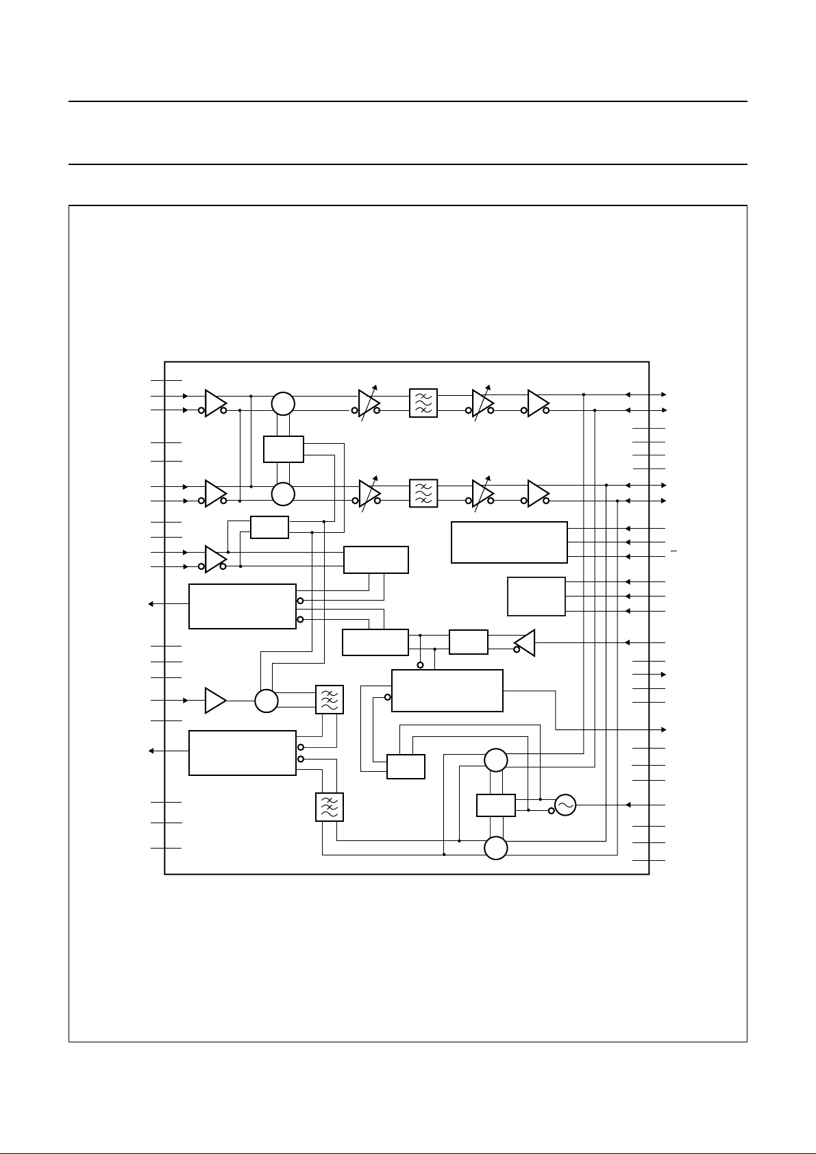
The receiver consists of two sections. The first section is
the RF receiver front-end, which amplifies the GSM, DCS
or PCS aerial signal, then converts the chosen channel
down to a low Intermediate Frequency (IF) of 100 kHz,
and also provides more than 35 dB image suppression.
Some selectivity is provided at this stage by an on-chip
low-passfilter andchannel selectivity isprovided bya high
performance integrated band-pass filter.
The second section is the IF section, which further
amplifies the chosen channel and performs gain control to
adjust the output level to the desired value. The IF gain
can be varied over more than 64 dB gain range.
The transmitteralso consists oftwo sections. The first is a
highprecision I/Q modulatorwhichconverts thebaseband
modulation up to the transmit IF. The second is a
modulation loop architecture which converts the signal
to RF.
The Local Oscillator (LO) signals are provided by an
on-chip Voltage Controlled Oscillator (VCO) for operation
of the IF section and are provided externally for operation
ofthe RF section.The frequenciesof theRF and IF VCOs
are set by internal PLL circuits, which are programmable
via a 3-wire serial bus. Comparison frequencies are
200 kHz (100 kHz step programmability) and 13 MHz for
the RF and IF PLL respectively, and are derived from a
13 MHz reference signal which has to be supplied
externally. The quadrature-phase RF LO signals required
for I/Q mixers in reception are generated internally.
The quadrature LO signals required for operation of the
I/Q modulator are generated inside the IF VCO.
The circuit can be powered-up into one of three different
modes: RX, TX or SYN mode, depending on the logic
state of pins RXON, TXON and SYNON, respectively. It is
also possible to set the IC in one of these modes by
software, using the 3-wire bus serial programming.
In RX (TX) mode, all sections required for receive
(transmit) are turned on. The SYN mode is used to
power-up the synthesizers prior to the RX or TX mode.
In the SYN mode, some internal LO buffers are also
powered-up in such a way that VCO pulling is minimized
when switching on the receiver or the transmitter.
Additional band selection is done using the 3-wire bus
serial programming, allowing the required enabling of the
Low Noise Amplifiers (LNAs) and charge pumps current
programming.
ORDERING INFORMATION
TYPE
NUMBER
UAA3535HL LQFP48 plastic low profile quad flat package; 48 leads; body 7 × 7 × 1.4 mm SOT313-2
2000 Feb 17 2
NAME DESCRIPTION VERSION
PACKAGE
Page 3
Philips Semiconductors Objective specification
Low power GSM/DCS/PCS multi-band transceiver UAA3535HL
BLOCK DIAGRAM
handbook, full pagewidth
RFGND1
GSMIA
GSMIB
RFGND2
V
CC(RF)
DCSPCSIA
DCSPCSIB
RFLOGND
V
CC(RFLO)
RFLOIA
RFLOIB
RFCPO
RFCPGND
V
CC(RFCP)
RFGND3
TXRFI
V
CC(TXCP)
TXCPO
TXCPGND
RFGND4
EXTRES
38
39
40
41
37
42
43
29
32
30
31
PHASE-FREQUENCY
24
DETECTOR AND
CHARGE PUMP
23
26
44
45
2
PHASE-FREQUENCY
1
DETECTOR AND
CHARGE PUMP
48
46
47
UAA3535HL
QUAD
1 : 1/2
×
7
IA
36
35
34
33
10
16
17
18
11
12
25
22
14
15
20
21
19
13
28
27
FCA074
8
9
3
5
4
6
IB
IFCIA
IFCIB
IFCQA
IFCQB
QA
QB
DATA
CLK
E
RXON
TXON
SYNON
REFIN
TXIFA
TSTO
V
CC2(IF)
IFGND2
IFCPO
IFCPGND
V
CC(IFCP)
IFGND1
IFTUNE
V
CC1(IF)
SYNGND
V
CC(SYN)
×
×
3-WIRE BUS
MAIN
DIVIDER
REFERENCE
DIVIDER
1 : 6/7
PHASE-FREQUENCY
DETECTOR AND
CHARGE PUMP
CONTROL REGISTER
POWER
ENABLE
1 : 1/2
×
1 : 1/2
91 MHz GSM/DCS
78 MHz PCS
×
Fig.1 Block diagram.
2000 Feb 17 3
Page 4
Philips Semiconductors Objective specification
Low power GSM/DCS/PCS multi-band transceiver UAA3535HL
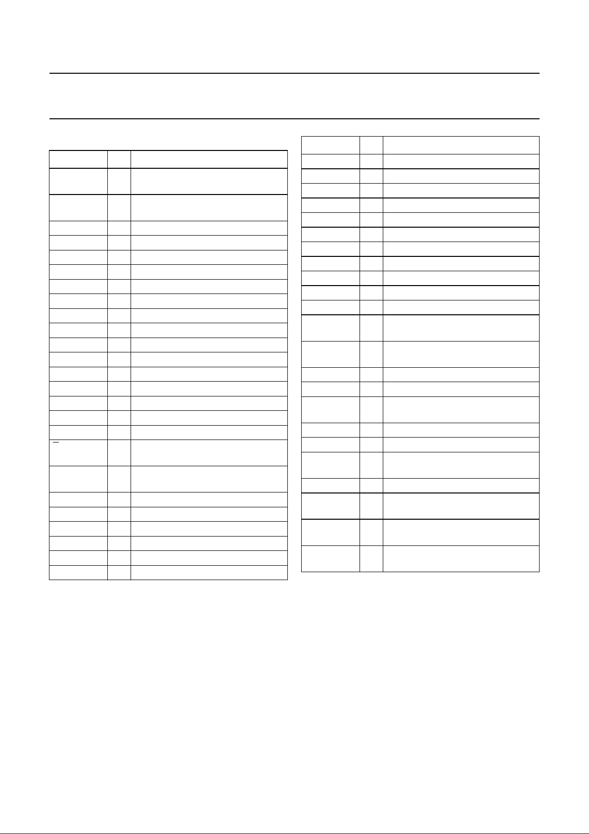
PINNING
SYMBOL PIN DESCRIPTION
TXCPO 1 transmit modulation loop GSM
charge pump output
V
CC(TXCP)
2 transmit modulation loop charge
pump supply voltage
TXIFA 3 transmit IF test pin
IFGND1 4 IF ground 1
TSTO 5 test mode output
V
CC1(IF)
6 IF supply voltage 1
IA 7 I path A baseband input/output
IB 8 I path B baseband input/output
QA 9 Q path A baseband input/output
QB 10 Q path B baseband input/output
RXON 11 RX mode control input
TXON 12 TX mode control input
IFTUNE 13 transmit IF VCO tune input
V
CC2(IF)
14 IF supply voltage 2
IFGND2 15 IF ground 2
DATA 16 3-wire bus data input
CLK 17 3-wire bus clock input
E 18 3-wire bus enable control input
(active LOW)
V
CC(IFCP)
19 transmit IF charge pump supply
voltage
IFCPO 20 transmit IF charge pump output
IFCPGND 21 transmit IF charge pump ground
REFIN 22 synthesizers reference input
RFCPGND 23 RF charge pump ground
RFCPO 24 RF charge pump output
SYNON 25 SYN mode control input
SYMBOL PIN DESCRIPTION
V
CC(RFCP)
V
CC(SYN)
26 RF charge pump supply voltage
27 synthesizers supply voltage
SYNGND 28 synthesizers ground
RFLOGND 29 RF LO ground
RFLOIA 30 RF LO input A
RFLOIB 31 RF LO input B
V
CC(RFLO)
32 RF LO supply voltage
IFCQB 33 RX IF Q test pin B
IFCQA 34 RX IF Q test pin A
IFCIB 35 RX IF I test pin B
IFCIA 36 RX IF I test pin A
V
CC(RF)
37 RF front-end and transmit
modulation loop supply voltage
RFGND1 38 RF front-end and transmit
modulation loop ground 1
GSMIA 39 receiver GSM RF input A
GSMIB 40 receiver GSM RF input B
RFGND2 41 RF front-end and transmit
modulation loop ground 2
DCSPCSIA 42 receiver DCS/PCS RF input A
DCSPCSIB 43 receiver DCS/PCS RF input B
RFGND3 44 RF front-end and transmit
modulation loop ground 3
TXRFI 45 input from RF transmit VCOs
RFGND4 46 RF front-end and transmit
modulation loop ground 4
EXTRES 47 reference resistor for transmit
modulation loop
TXCPGND 48 transmit modulation loop charge
pump ground
2000 Feb 17 4
Page 5
Philips Semiconductors Objective specification
Low power GSM/DCS/PCS multi-band transceiver UAA3535HL
handbook, full pagewidth
TXCPO
V
CC(TXCP)
TXIFA
IFGND1
TSTO
V
CC1(IF)
RXON
TXON
QA
QB
RFGND4
EXTRES
47
46
14
15
IFGND2
CC2(IF)
V
TXRFI
RFGND3
45
44
UAA3535HL
16
17
CLK
DATA
TXCPGND
48
1
2
3
4
5
6
IA
7
IB
8
9
10
11
12
13
IFTUNE
DCSPCSIA
DCSPCSIB
43
42
18
19
E
CC(IFCP)
V
RFGND2
GSMIB
41
40
21
20
IFCPO
IFCPGND
RFGND1
GSMIA
39
38
22
23
REFIN
RFCPGND
CC(RF)
V
24 37
RFCPO
36
IFCIA
35
IFCIB
34
IFCQA
33
IFCQB
V
32
31
RFLOIB
RFLOIA
30
29
RFLOGND
SYNGND
28
V
27
V
26
SYNON
25
FCA068
CC(RFLO)
CC(SYN)
CC(RFCP)
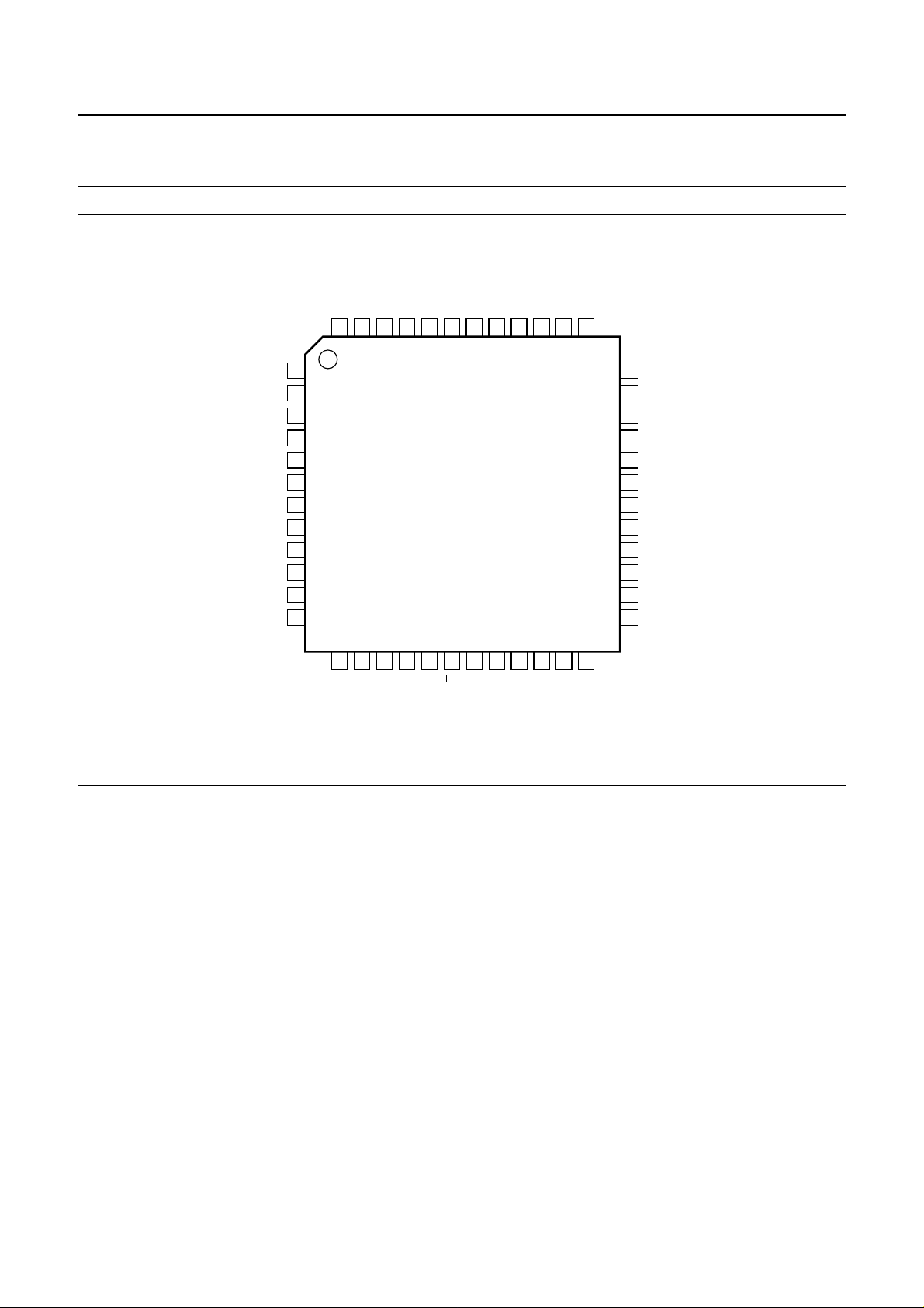
Fig.2 Pin configuration.
FUNCTIONAL DESCRIPTION
RF receiver
The receiver front-end converts the aerial RF signal from
EGSM (Extended GSM; 925 to 960 MHz), DCS
(1805 to 1880 MHz) or PCS (1930 to 1990 MHz) bands
down to an IF signal of 100 kHz. The first stages are
symmetricalLNAs thatarematched to50 Ωusing external
baluns. The LNAs are followed by an I/Q down-mixer.
The I/Q down-mixer consists of two mixers in parallel but
driven by quadrature out of phase LO signals.
The In-phase (I)and Quadrature- phase (Q)IF signalsare
then low-pass filtered to provide protection from high
frequency offset interferers. The IF I and Q signals are
then fed into the channel filter.
2000 Feb 17 5
Channel filter and AGC
The front-end IF I and Q outputs are first applied to an
amplifier circuit with provision for three 8 dB gain step
adjustment possibilities and then to an integrated
band-pass channel filter. The filter is a fifth-order
band-pass filter centred around 100 with 220 kHz
bandwidth. After filtering the IF I and Q signals are further
amplified with provision for eleven 4 dB gain steps and
DC offset compensation.
I/Q modulator
I and Q baseband signals are applied to the I/Q modulator
where the modulation spectrum is shifted up to the
transmit IF frequency. For low harmonic distortion, low
carrier leakage and high image rejection, the phase error
must be kept as small as possible. The IF output of the
modulator is fed to an integrated low-pass filter where
unwanted spurious signals are suppressed, prior to being
fed to the phase detector.
Page 6
Philips Semiconductors Objective specification
Low power GSM/DCS/PCS multi-band transceiver UAA3535HL
Transmit modulation loop
The analog transmit modulation loop consists of an
on-chip offset mixer, a phase-frequency detector, an
off-chip loop filter and a transmit VCO. The analog PLL
copies the modulation to the off-chip transmit VCO and
acts as a tracking filter. A PLL of at least third-order is
requiredto meet noiserequirements at 20 MHzoffset from
the carrier. The PLL bandwidth must be greater than
600 kHz in orderto keepa lowdynamic phase error and to
minimize the acquisition time.
RF and IF LO sections
The RF LO input covering the 1788 to 2002 MHz
bandwidth is connected to an external RF VCO module.
The RF LO section includes the LO buffering for the
RF PLL, a divider-by-2 or 1 for GSM and DCS/PCS
respectivelywhich drives aquadraturegeneration network
for use in the RX I/Q down-mixer or the transmit
modulationloop offset mixer. TheIF LOsection consists of
a fully integrated IF VCO which internally provides the
I/Q modulator with the necessary quadrature signals.
Dual PLL
A high performance dual PLL is included on-chip which
enables the frequencies of the RF VCO to be synthesized
off-chip and that of the IF VCO on-chip. Very low close-in
phase noise is achieved which allows the PLL loop
bandwidthto be widenedto achieve ashortersettling time.
The charge pump circuit has very low leakage current, in
the nA range, so that the spurious signals are hardly
detectable.
The ‘main’ path consists of a programmable divider chain
that divides the RF and IF LO signals down to frequencies
of 200 kHz (100 kHz step programmability) and 13 MHz
respectively. Their phase is then compared in a digital
Phase-Frequency Detector (PFD) with that of a reference
signal derived from an external 13 or 26 MHz clock signal.
The phase error information is fedback tothe VCOvia the
charge pump circuit that ‘sinks’ into or ‘sources’ current
from the loop filter capacitor, thereby changing the VCO
frequency so that the loop becomes ‘phase locked’.
Operating modes
BASIC OPERATING MODES
The circuit can be powered-up into different operating
modes depending on the voltage level applied at pins
RXON, TXON and SYNON (hardware control). This
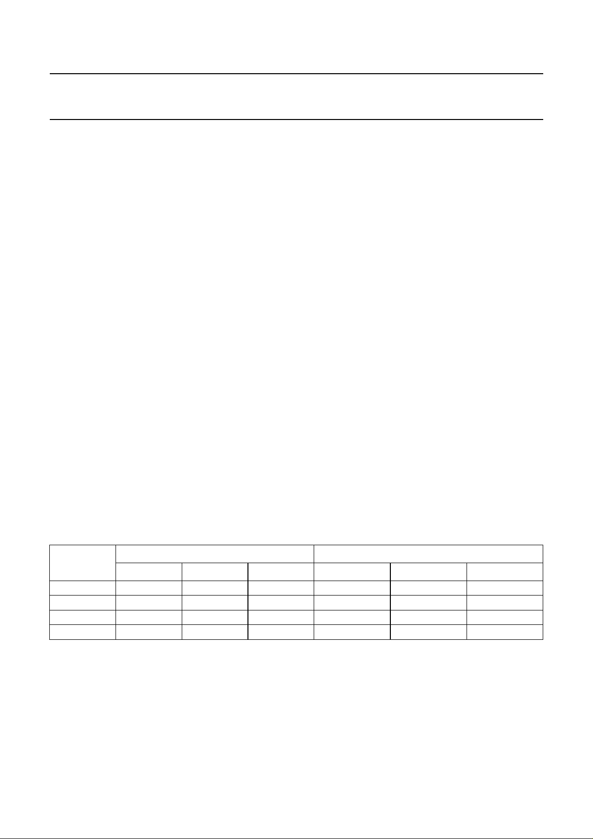
defines the three main modes; RX, TX and SYN. Table 1
describes the different operating modes as defined by
hardware control.
The operation mode status depends on the control bits
SYNON, RXON and TXON (see Table 1).
When the receiver is on, it is possible to switch-off the low
noise amplifier to perform DC offset compensation in the
receiver (see Section “LNA power control”).
When in TX mode, it is possible to enable the
IF synthesizer and VCOindependently fromthe rest of the
TX section via bit TXIFON via the control bus.
Table 1 Basic operating mode control
MODE
SYNON RXON TXON SYNTHESIZER RECEIVER TRANSMITTER
SYN HIGH LOW LOW on off off
RX HIGH HIGH LOW on on off
TX HIGH LOW HIGH on off on
Idle LOW LOW LOW off off off
2000 Feb 17 6
CONTROL PIN LEVEL POWER STATUS
Page 7
Philips Semiconductors Objective specification
Low power GSM/DCS/PCS multi-band transceiver UAA3535HL
IF SYNTHESIZER AND VCO CONTROL
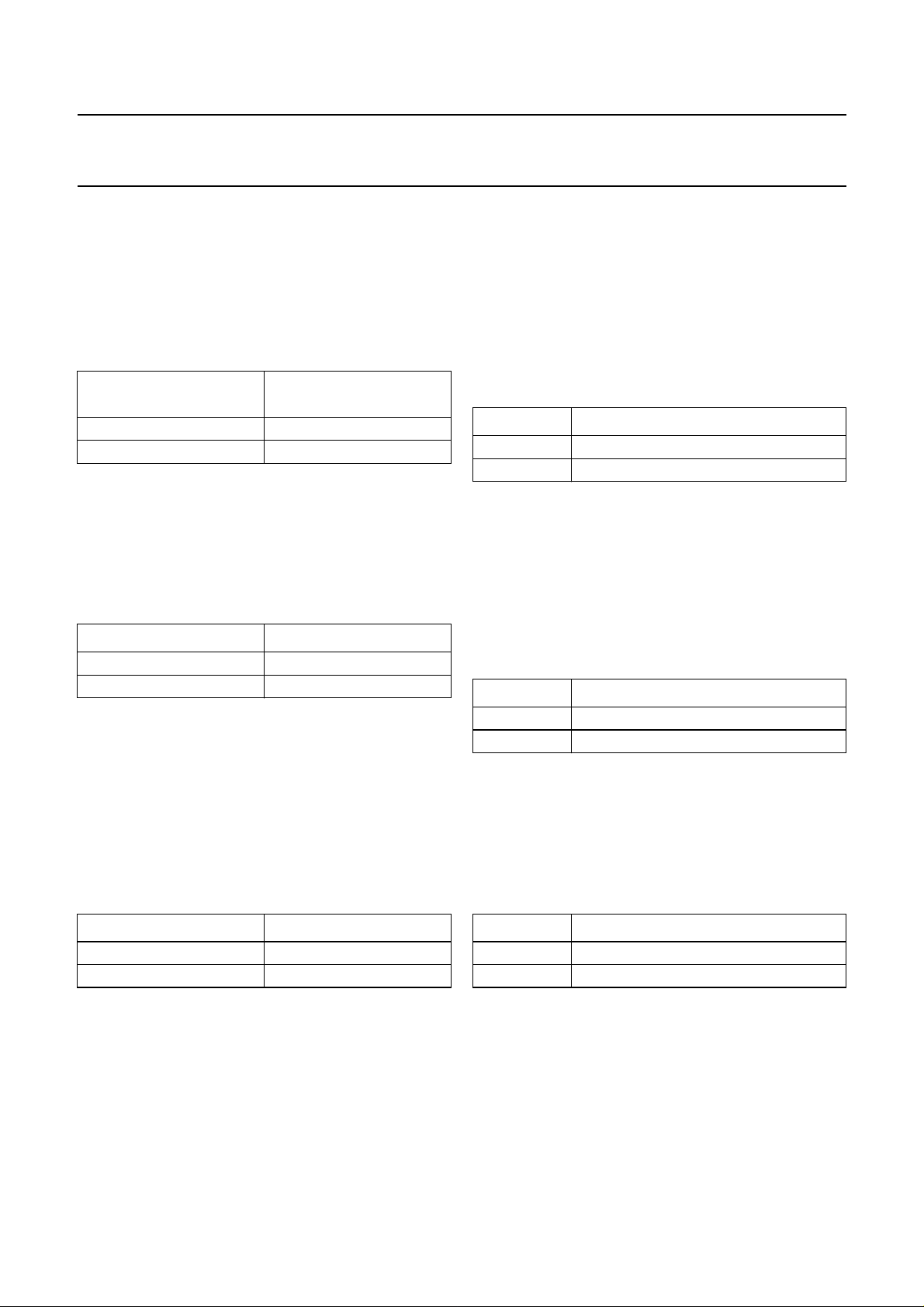
The IF synthesizer is only necessary in transmit mode.
The TX IF VCO and synthesizer section can be
powered-up with the control bit TXIFON; see Table 2.
If TXIFONis not used,the IF VCO andsynthesizer section
will be enabled with the signal TXON.
Table 2 IF synthesizer and VCO power control
BIT TXIFON
0 off
1on
LNA POWER CONTROL
When the receiver is on, it is possible to switch-off the low
noise amplifier separately. Separate control of the low
noise amplifier isaccomplished bythe control bit LNA; see
Table 3.
Table 3 LNA power control
BIT LNA LNA MODE
0 off
1on
BAND SELECTION CONTROL
The receiver includes two RF front-end and RF LO
sections; one for GSM where the RF LO is divided-by-2
and fed to the 925 to 960 MHz front-end, and the other
one for DCS and/or PCS where the RF LO is not divided
and fedto the 1805 to 1990 MHz front-end. The selection
of these 2 modes is accomplished by the control bit BND;
see Table 4.
IF SYNTHESIZER AND
VCO MODE
SIDEBAND SELECTION CONTROL
The receiver includes an image rejection front-end which
allows the use of a RF LO 100 kHz below the RF input
frequency (infradyne) or 100 kHz above the RF input
frequency (supradyne). Between these two states the
proper image should be selected for rejection.
The selection of these 2 modes is accomplished by the
control bit SBD; see Table 5.
Table 5 Sideband selection control
BIT SBD SIDEBAND MODE
0 supradyne
1 infradyne
TX CHARGE PUMP CURRENT CONTROL
The transmit modulation loop includes a transmit charge
pump where sink and source currents are determined by
an external resistor. When determined, this nominal
current can be divided-by-1 or 2 to cope with different
transmit VCO gains. The selection of these 2 modes is
accomplished by the control bit TXI; see Table 6.
Table 6 TX charge pump current control
BIT TXI TX CHARGE PUMP CURRENT MODE
0 nominal current
1 nominal current divided-by-2
REFERENCE DIVIDER CONTROL
The reference divider can be programmed to divide the
external reference frequency by 65 or 130. The selection
of these 2 modes is accomplished by the control bit
REFDIV; see Table 7.
Table 4 Band selection control
BIT BND BAND MODE
0 GSM
1 DCS and/or PCS
2000 Feb 17 7
Table 7 Reference divider control
BIT REFDIV REFERENCE DIVIDER MODE
0 divide-by-65
1 divide-by-130
Page 8
Philips Semiconductors Objective specification
Low power GSM/DCS/PCS multi-band transceiver UAA3535HL
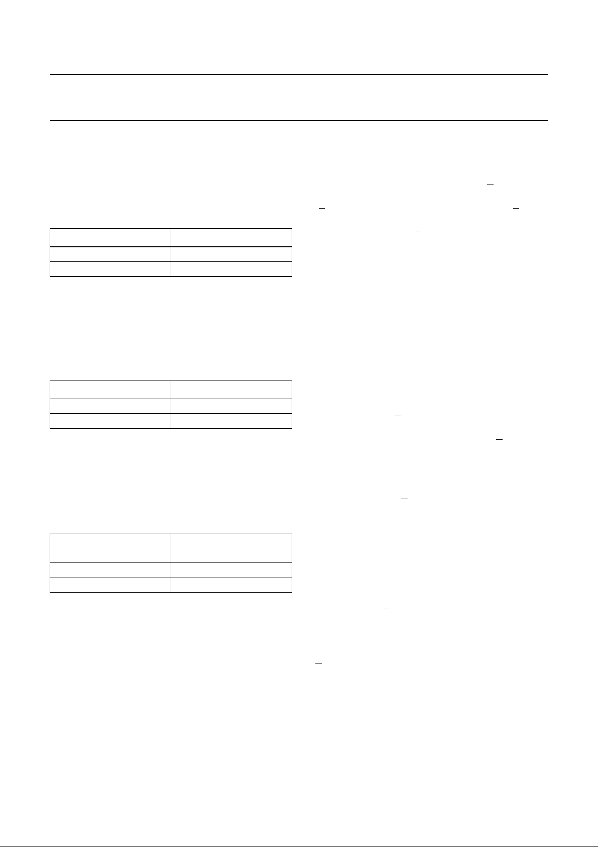
IF DIVIDER CONTROL
The IF divider can be programmed to divide the integrated
IF VCO frequency by 1 or 2. The selection of these
2 modes is accomplished by the control bit IFDIV;
see Table 8.
Table 8 IF divider control
BIT IFDIV IF DIVIDER MODE
0IF=f
1IF=f
VCO
divided by 2
VCO
TXIF FILTER CONTROL
The transmit section integrates two switchable low-pass
filters, one for a 45.5 MHz IF and the other one for
91 MHz IF. The selection of these 2 modes is
accomplished by the control bit FILT; see Table 9.
Table 9 TXIF filter control
BIT FILT TXIF FILTER MODE
0 IF 45.5 MHz
1 IF 91 MHz
IF SYNTHESIZER DIVIDER CONTROL
The IF synthesizer divider can be programmed to divide
the semi-integrated IF VCO frequency by 6 or 7.
The selection of these 2 modes is accomplished by the
control bit IFO; see Table 10.
Programming
SERIAL PROGRAMMING BUS
Asimple3-wire unidirectional serialbusisused to program
the circuit. The 3 lines are DATA, CLK and E (enable).
The data sent to the device is loaded in bursts framed
by E. Programming clock edges are ignored until E goes
active LOW. The programmed information is loaded into
the addressed latch whenE returns inactive HIGH. This is
allowed when CLK is in either state without causing any
consequences to the register data. Only the last 17 bits
serially clocked into the device are retained within the
programming register. Additional leading bits are ignored,
and no check is made on the number of clock pulses.
The fully static CMOS design uses virtually no current
when the bus is inactive. It can always capture new
programming data even during power-down of both
synthesizers.
DATA FORMAT
Data is entered with the most significant bit first.
The leading bits make up the data field, while the trailing
4 bits are an address field. The address bits are decoded
on the rising edge of E. This produces an internal load
pulse to store the data in the addressed latch. To ensure
that data is correctly loaded on first power-up, E should be
held LOW and only taken High after having programmed
an appropriate register. To avoid erroneous divider ratios,
the pulse is inhibited during the period when data is read
by the frequency dividers. This condition is guaranteed by
respecting a minimum E pulse width after data transfer.
Table 10 IF synthesizer divider control
BIT IFO
IF SYNTHESIZER
DIVIDER MODE
0 divide-by-6
1 divide-by-7
2000 Feb 17 8
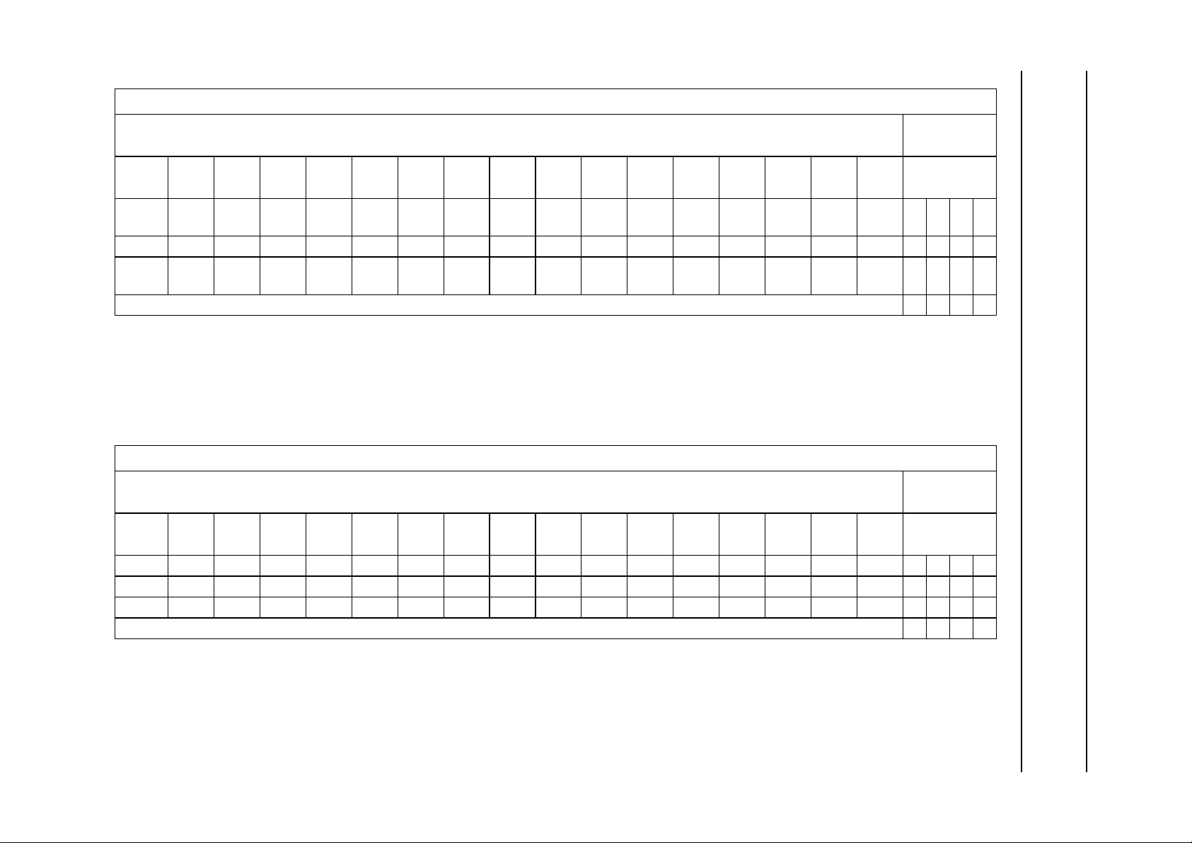
The allocation of the register bits is given in Table 11.
REGISTER PRESET CONDITIONS
The UAA3535HL programming registers have a preset
state. The preset values can be found in Table 12.
Conditions for guaranteed preset values at power-on are
as follows:
• DATA, CLOCK, E, SYNON, RXON and TXON must be
at 0 V
• Preset value is guaranteed 2 ms after V
CC(SYN)
rises
to 90% of 2.6 V
• E should stay at 0 V up to the end of the first
programming word.
Page 9
2000 Feb 17 9
Table 11 Register bit allocation; notes 1 and 2 and 3
Philips Semiconductors Objective specification
Low power GSM/DCS/PCS multi-band transceiver UAA3535HL
REGISTER ALLOCATION
LAST 4 BITS
0
LAST 4 BITS
0
ADDRESS
FIELD
ADDRESS
FIELD
DATA FIELD
BIT16BIT15BIT14BIT13BIT12BIT11BIT10BIT9BIT8BIT7BIT6BIT5BIT4BIT3BIT2BIT1BIT
XXRF14RF13RF12RF
11
XXXXX00000LNAG5G4G3G2G1G00010
X X X 0 FILT REF
DIV
for test purpose only; bit usage to be defined; this is a forbidden address 0000
Notes
1. The 15-bit RF divider is programmable through the 15 bits RF0 to RF14, in steps of 100 kHz.
2. X = don’t care.
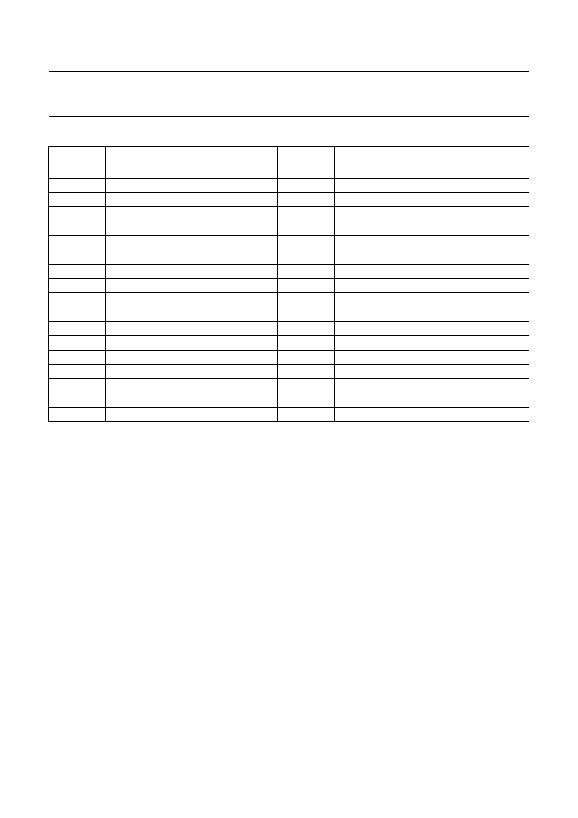
3. The 6-bit AGC attenuator is programmable through the 6 bits G0 to G5 in 17 steps of 4 dB (see Table 13).
Table 12 Preset values; note 1
BIT16BIT15BIT14BIT13BIT12BIT11BIT10BIT9BIT8BIT7BIT6BIT5BIT4BIT3BIT2BIT1BIT
XX1001010000001100011
XXXXX0000011111110010
XXX000110101100000001
for test purpose only; bit usage to be defined; this is a forbidden address 0000
RF10RF
IFO IF
DIV
RF8RF7RF6RF5RF4RF3RF2RF1RF00011
9
TXI SBD BND 1 1 TXIFONSYNONRXONTXON0001
REGISTER ALLOCATION
DATA FIELD
Note
1. X = don’t care.
Page 10
Philips Semiconductors Objective specification
Low power GSM/DCS/PCS multi-band transceiver UAA3535HL
Table 13 AGC gain look-up table; note 1
(2)
G5
111111 0
111110 4
101111 8
101110 12
011111 16
011110 20
011101 24
011100 28
010111 32
010110 36
000111 40
000110 44
000101 48
000100 52
000011 56
000010 60
000001 64
000000 68
G4
(2)
G3 G2 G1 G0 ATTENUATION (dB)
(3)
Notes
1. Codes not included in the table are forbidden.
2. Steps at the input of the band-pass filter.
3. The figure represents the total attenuation in the receive path, with respect to the maximum gain.
2000 Feb 17 10
Page 11
Philips Semiconductors Objective specification
Low power GSM/DCS/PCS multi-band transceiver UAA3535HL
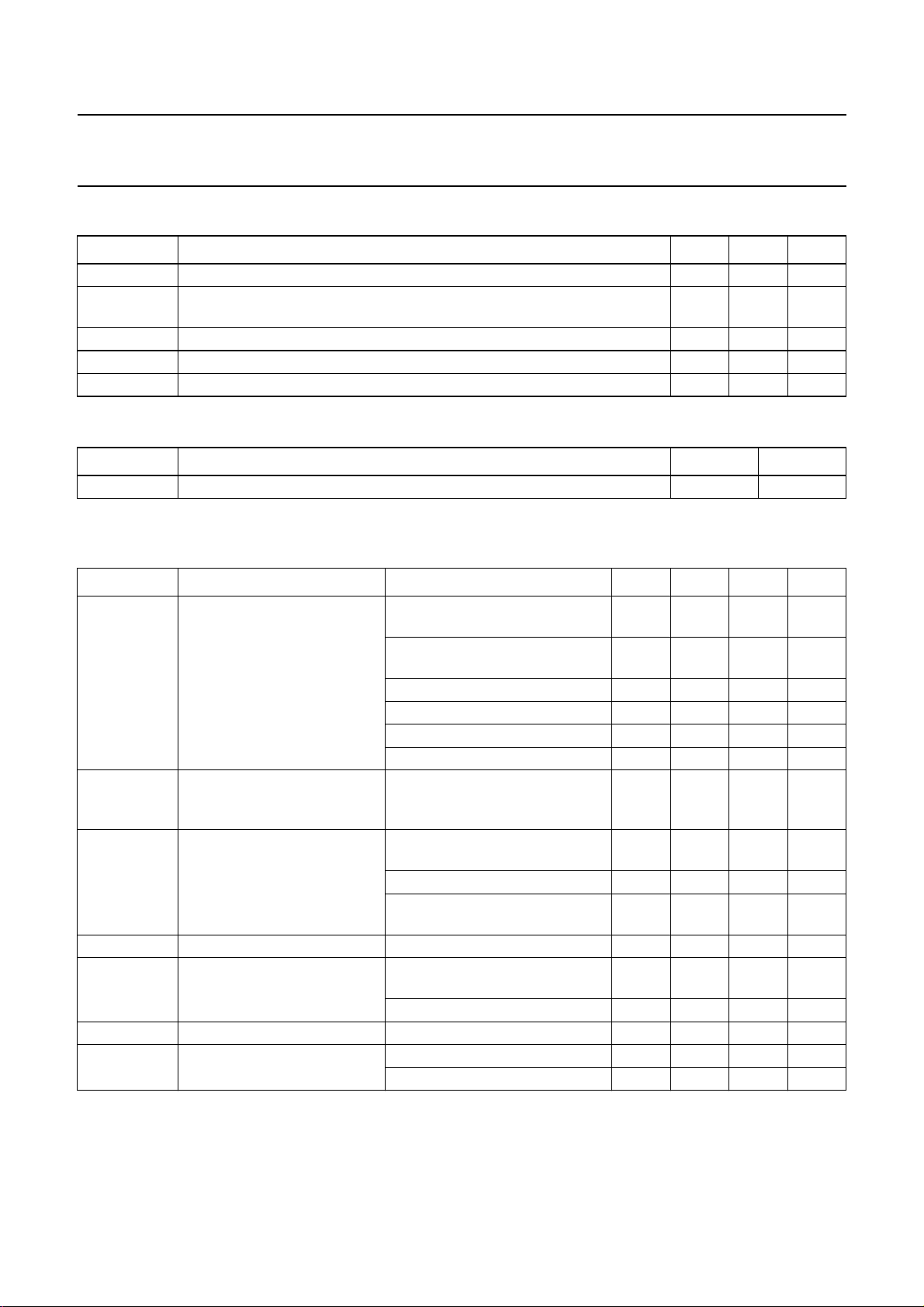
LIMITING VALUES
SYMBOL DESCRIPTION MIN. MAX. UNIT
V
CC
V
CC(TXCP)
V
CC(RFCP)
P
max
T
amb
T
stg
THERMAL CHARACTERISTICS
SYMBOL PARAMETER VALUE UNIT
R
th(j-c)
DC CHARACTERISTICS
VCC=V
CC(TXCP)=VCC(RFCP)
supply voltage −0.3 +3.6 V
;
supply voltage for RX and TX charge pumps −0.3 +4.25 V
maximum power dissipation − 1W
ambient temperature −30 +70 °C
storage temperature −40 +150 °C
thermal resistance from junction to case 65 K/W
= 2.6 V; T
=25°C; unless otherwise specified.
amb
SYMBOL PARAMETER CONDITIONS MIN. TYP. MAX. UNIT
I
CC
supply current normal mode; total power-down;
− 10 50 µA
note 1
preset mode; total power-down;
− 100 200 µA
note 2
RX and SYN mode − 51.5 60 mA
TX, TXIF and SYN mode − 54 66 mA
SYN mode − 17 20 mA
TXIF and SYN mode − 29 37 mA
V
CC(RF)
RF front-end and transmit
2.4 − 3.3 V
modulation loop supply
voltage
I
CC(RF)
RF front-end and transmit
modulation loop supply
current
RX mode; one LNA and
− 17 − mA
quadrature mixer active
RX mode; one LNA active − 6 − mA
TX mode; transmit modulation
− 6 − mA
loop active without charge pump
V
CC1(IF)
I
CC1(IF)
IF supply voltage 1 2.4 − 3.3 V
IF supply current 1 RX mode; I/Q low IF band-pass
− 7 − mA
filter active
TX mode; I/Q modulator active − 9 − mA
V
CC2(IF)
I
CC2(IF)
IF supply voltage 2 2.4 − 3.3 V
IF supply current 2 RX mode; I/Q AGC active − 4 − mA
TXIF mode; TX IF VCO active − 9 − mA
2000 Feb 17 11
Page 12
Philips Semiconductors Objective specification
Low power GSM/DCS/PCS multi-band transceiver UAA3535HL
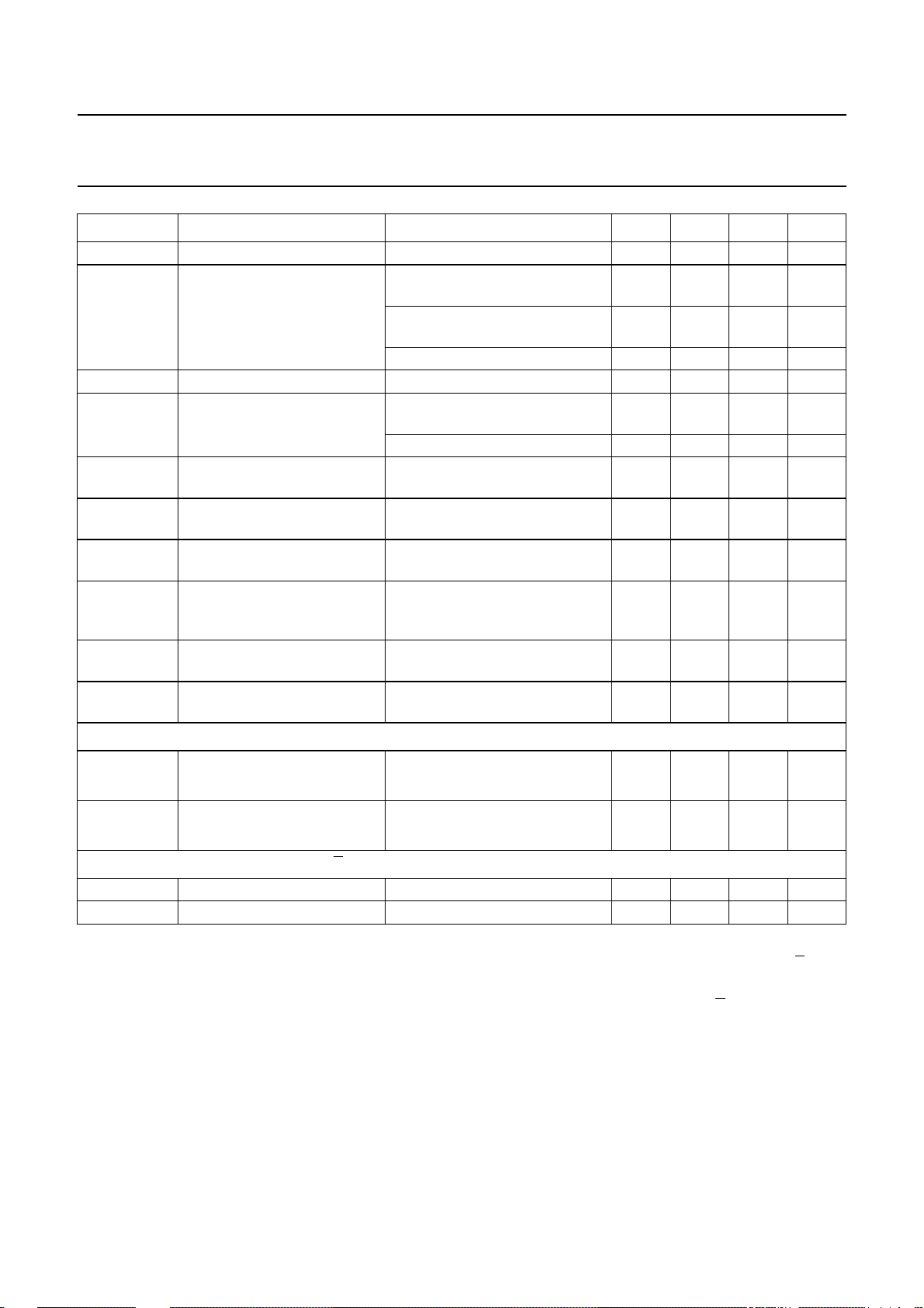
SYMBOL PARAMETER CONDITIONS MIN. TYP. MAX. UNIT
V
CC(RFLO)
I
CC(RFLO)
V
CC(SYN)
I
CC(SYN)
V
CC(IFCP)
I
CC(IFCP)
V
CC(TXCP)
I
CC(TXCP)
V
CC(RFCP)
I
CC(RFCP)
Baseband section: pins IA, IB, QA and QB
V
I(CM)
V
Q(CM)
RF LO supply voltage 2.4 − 3.3 V
RF LO supply current RX and SYN mode; RF LO buffer
− 10 − mA
and divider section active
TX and SYN mode; RF LO buffer
− 10 − mA
and divider section active
SYN mode; RF LO buffer active − 6 − mA
synthesizers supply voltage 2.4 − 3.3 V
synthesizers supply current SYN mode; RF synthesizer
− 9.5 − mA
active
TXIF mode; IF synthesizer active − 0.5 − mA
transmit IF charge pump
2.4 − 3.3 V
supply voltage
transmit IF charge pump
supply current
transmit modulation loop
TXIF mode; IF LO charge pump
active; in lock
− 1.5 − mA
2.4 − 4.25 V
charge pump supply voltage
transmit modulation loop
charge pump supply current
TX mode; TX RF charge pump
active; in lock; external
− 1.0 − mA
resistance is 1800 Ω
RF charge pump supply
2.4 − 4.25 V
voltage
RF charge pump supply
current
common mode input-output
voltage I
common mode input-output
voltage Q
SYN mode; RF LO charge pump
active; in lock
VIAVIB+
=
V
----------------------- -
I
V
Q
2
V
QAVQB
=
----------------------------
+
2
− 4.5 − mA
1.15 1.25 1.35 V
1.15 1.25 1.35 V
Logic input levels: pins DATA, CLK,
V
IH
V
IL
HIGH-level input voltage 0.9 −−V
LOW-level input voltage −−0.3 V
E, TXON, RXON and SYNON
Notes
1. V
CC(TXCP)=VCC(RFCP)
= 4.2 V; pins TXON, RXON and SYNON are HIGH impedance; pins DATA, CLK and E are
HIGH impedance.
2. V
CC(TXCP)=VCC(RFCP)
= 4.2 V; pins TXON, RXON and SYNON are LOW; pins DATA, CLK and E are HIGH.
2000 Feb 17 12
Page 13
Philips Semiconductors Objective specification
Low power GSM/DCS/PCS multi-band transceiver UAA3535HL
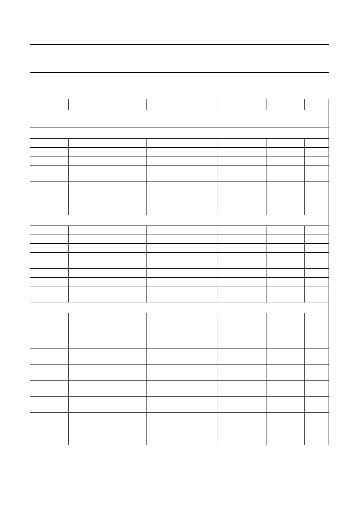
AC CHARACTERISTICS
VCC=V
SYMBOL PARAMETER CONDITIONS MIN. TYP. MAX. UNIT
RF receiver section; measured in a 50 Ω impedance system, including external input baluns and matching
networks to 50 Ω
INS: GSMIA AND GSMIB
P
f
i(RF)
R
i(dif)
C
i(dif)
F noise figure for R
α
off
P
off
DES3
i
PINS: DCSPCSIA AND DCSPCSIB
f
i(RF)
R
i(dif)
C
i(dif)
F noise figure for R
α
off
P
off
DES3
i
PINS: GSMIA, GSMIB, DCSPCSIA AND DCSPCSIB
s
11
SPUR
P(RFin)
CP1 1 dB input compression point minimum AGC;
IP3
i
IP2
i
DES3
i
IR image rejection f
∆G
v(RF)
CC(CP)
= 2.6 V; T
= −30 to +70 °C; unless otherwise specified.
amb
RF input frequency 925 − 960 MHz
differential input resistance parallel RC input model − 75 −Ω
differential input capacitance parallel RC input model − 1.5 − pF
; maximum AGC;
i
− 3.5 4 dB
notes 1 and 2
LNA off-state attenuation bit LNA = 0; note 1 − 45 − dB
LNA off-state power handling bit LNA = 0; notes 1 and 3 3 −− dBm
input referred 3 dB
desensitization
∆f = 3 MHz; T
note 1
amb
=25°C;
−25 −− dBm
RF input frequency 1805 − 1990 MHz
differential input resistance parallel RC input model − 120 −Ω
differential input capacitance parallel RC input model − 1.0 − pF
; maximum AGC;
i
− 4 4.5 dB
notes 1 and 2
LNA off-state attenuation bit LNA = 0; note 1 − 45 − dB
LNA off-state power handling bit LNA = 0; notes 1 and 3 6 −− dBm
input referred 3 dB
desensitization
∆f = 3 MHz; T
note 1
amb
=25°C;
−28 −− dBm
input reflection coefficient note 2 −−15 −10 dB
power level of spurious
signals at RF input
900 to 1000 MHz band −−−57 dBm
1800 to 2000 MHz band −−−47 dBm
out of preceding bands −−−45 dBm
−25 −− dBm
=25°C; note 1
T
amb
input referred third-order
intercept
input referred second-order
maximum AGC;
T
=25°C; note 1
amb
−18 −− dBm
maximum AGC; note 4 − 30 − dBm
intercept
input referred 3 dB
desensitization
gain mismatch GSM and
∆f = 3 MHz; T
amb
=25°C;
−23 −− dBm
note 1
= 200 kHz;
IF
T
=25°C; note 1
amb
35 38 − dB
note 5 −−2dB
DCS paths
2000 Feb 17 13
Page 14
Philips Semiconductors Objective specification
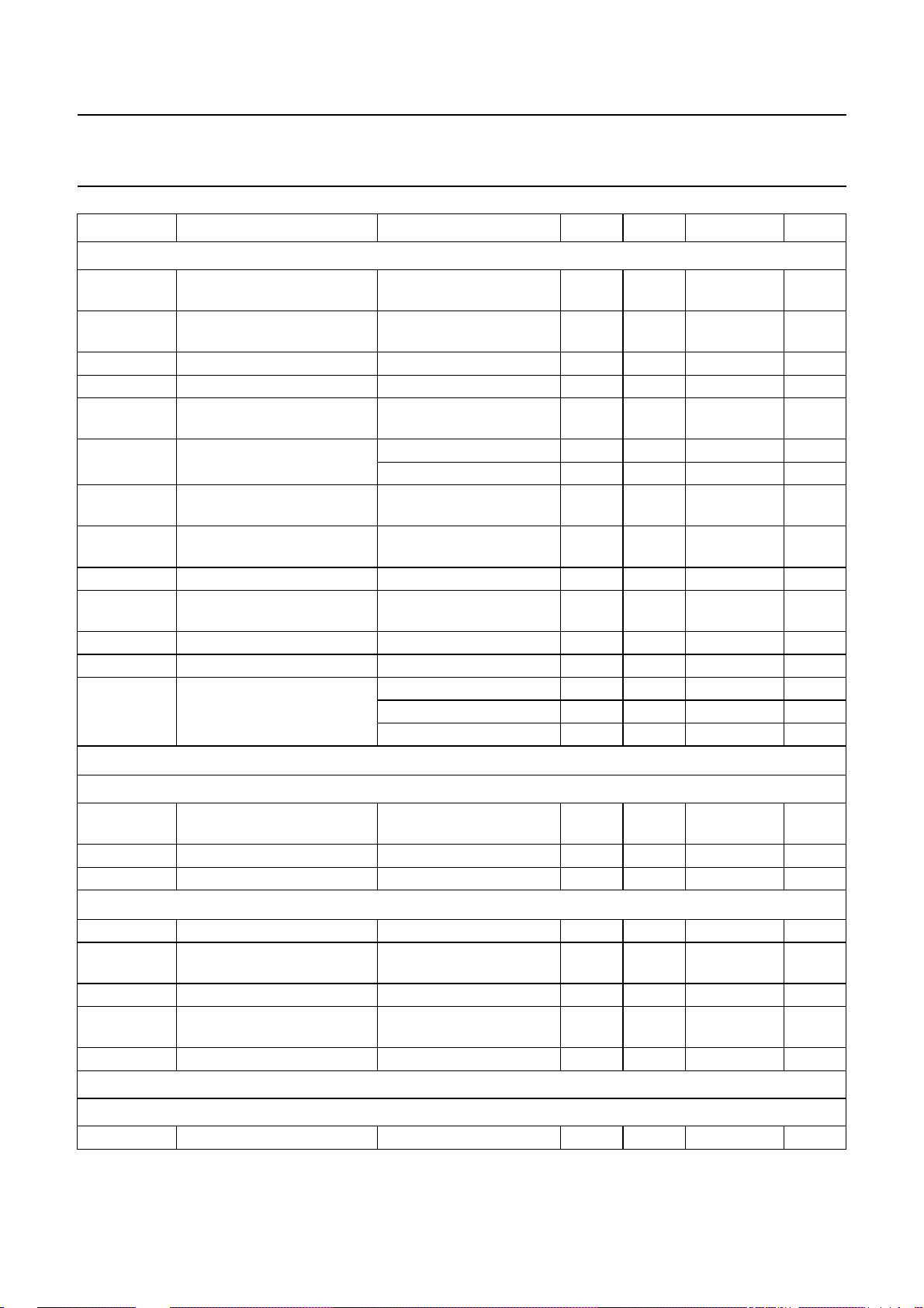
Low power GSM/DCS/PCS multi-band transceiver UAA3535HL
SYMBOL PARAMETER CONDITIONS MIN. TYP. MAX. UNIT
PINS IA, IB, QA AND QB (RX MODE)
G
v(min)
minimum voltage conversion
gain
G
v(max)
maximum voltage conversion
gain
G
∆G
v(step)
v(I/Q)
voltage conversion gain step note 5 − 4 − dB
gain mismatch I and Q paths note 5 −−0.5 dB
∆Φ quadrature-phase error
I and Q paths
LE
V
o(peak)
AGC
gain control linearity over full gain range; note 2 −2 − +2 dB
maximum output voltage per
pin
I
o(peak)
maximum output current per
pin
V
offset
HP
−3dB
output offset voltage under static conditions −300 − +300 mV
−3 dB high-pass corner
frequency
B
IF(−3dB)
∆t
d(g)
α
5(IF)
−3 dB IF filter bandwidth 100 kHz centre frequency 220 − 250 kHz
group delay variation 30 kHz < fo< 170 kHz − 1.5 2 µs
IF filter attenuation
(fifth-order)
Transmit IF section (initial conditions: V
gain set to minimum;
19 25 31 dB
notes 1 and 5
gain set to maximum;
89 93 97 dB
notes 1 and 5
peak error −−5 deg
over any 20 dB gain range −0.5 − +0.5 dB
3% T.H.D.; RL= 100 kΩ
0.75 −− V
per pin
25 50 −µA
468 kHz
fo= 100 kHz ± 200 kHz 17 31 − dB
f
= 100 kHz ± 400 kHz 54 64 − dB
o
f
= 100 kHz ± 600 kHz 73 82 − dB
o
mod(peak)
= 0.5 V; f
= 67.7 kHz; unless otherwise specified)
mod
P
INS IA, IB, QA AND QB (TX MODE)
f
mod
modulation frequency 3 dB low-pass cut-off
frequency
V
mod(peak)
R
i(D)
modulation level single-ended; peak value − 0.5 0.55 V
dynamic input resistance single-ended − 25 − kΩ
IF LO oscillator (measured and guaranteed on demonstration board at T
f
IFLO
K
VCO
range of possible operation with programming 78 − 91 MHz
VCO gain V
from 0.6 V to
tune
VCC− 0.6 V
V
∆f
tune
VCC
tuning voltage referenced to V
frequency variation with
pushing −−1 MHz/V
CC(IFCP)
respect to the supply voltage
∆f
TRON
frequency variation pulling −5 − +5 kHz
Transmit modulation loop section
OFFSET MIXER; PIN TXRFI
f
RF
RF input frequency 880 − 1910 MHz
2000 Feb 17 14
1 −− MHz
=25°C)
amb
− 30 − MHz/V
0.4 − VCC− 0.4 V
Page 15
Philips Semiconductors Objective specification
Low power GSM/DCS/PCS multi-band transceiver UAA3535HL
SYMBOL PARAMETER CONDITIONS MIN. TYP. MAX. UNIT
R
i
C
i
P
i
s
11
F noise figure T
CP1 1 dB input compression point T
SPUR
P(RFin)
P
HASE DETECTOR; PIN TXCPO
I
CP(max)
KΦ phase-frequency detector
∆KΦ phase-frequency detector
V
o
R
o
R
o(pd)
LO
o
IM3
o
IM
o
Φ
NOISE
SPUR
L(4fm)
SPUR
L(8fm)
RF LO buffer
input resistance single-ended − 50 −Ω
input capacitance single-ended −−− pF
input power −23 −20 −17 dBm
input reflection coefficient −−10 − dB
=25°C − 10 − dB
amb
=25°C −−20 − dBm
amb
power level of spurious
signals at RF input
charge pump maximum sink
or source current
LO leakage −−50 −45 dBm
other −−−45 dBm
GSM mode; external
124 mA
resistance of 1800 Ω 1%
for minimum output
current; TXI = 0; note 6
DCS and PCS mode;
0.5 1 2 mA
external resistance of
1800 Ω 1% for minimum
output current; TXI = 1;
note 6
=1mA − 0.16 − mA/rad
for I
CP
gain
over output voltage range −−10 %
gain variation
output voltage 0.4 − V
output resistance − 10 − kΩ
output resistance power
V
o
=
---------------------- -
CC(PHD)
2
V
TX mode disabled − 1 − kΩ
CC(CP)
− 0.4 V
down
local oscillator feedthrough note 7 −−40 −32 dBc
third-order products level offset +3 × 67.7 kHz or
−−55 −50 dBc
−3 × 67.7 kHz; note 7
image level f
phase noise output power
density
level of spurious signals at
4 × f
mod
level of spurious signals at
8 × f
mod
− 67.7 kHz; note 7 −−45 −37 dBc
IFLO
∆f = 400 kHz;
T
=25°C; note 7
amb
∆f = 1.8 MHz;
=25°C; note 7
T
amb
∆f = 20 MHz; T
f
= 67.7 kHz;
mod
=25°C −−−136 dBc/Hz
amb
−−−117 dBc/Hz
−−−117 dBc/Hz
−−−50 dBc
notes 7 and 8
f
= 67.7 kHz; note 7 −−−55 dBc
mod
RF SOURCE CONNECTED AT PIN RFLOIA AND RFLOIB
f
i(RF)
RF input frequency 1788 − 2002 MHz
2000 Feb 17 15
Page 16
Philips Semiconductors Objective specification
Low power GSM/DCS/PCS multi-band transceiver UAA3535HL
SYMBOL PARAMETER CONDITIONS MIN. TYP. MAX. UNIT
R
i(dif)
C
i(dif)
s
11
P
LO
RF and IF synthesizers
REFERENCE INPUT; PIN REFIN
f
ref
V
i(rms)
R
i
RF SYNTHESIZER; PIN RFCPO
f
RFLO
f
comp(RF)
f
comp(leak)
f
step(RF)
Φ
noise
SPUR
P(RF)
I
CP(nom)
KΦ phase-frequency detector
∆KΦ phase-frequency detector
I
L(CP)
V
CP
R
o
differential input resistance parallel RC input model − 50 −Ω
differential input capacitance parallel RC input model − 0.2 − pF
input reflection coefficient −−15 −10 dB
power available from the
−8 −5 −2 dBm
LO source
reference frequency REFDIV = 0 − 13 − MHz
REFDIV = 1 − 26 − MHz
input voltage level
60 − 220 mV
(RMS value)
input resistance f
= 13 MHz − 10 − kΩ
ref
synthesizer frequency 1700 − 2100 MHz
comparison frequency − 200 − kHz
200 kHz comparison
frequency leakage
frequency step
with recommended loop
filter
f
comp(RF)
= 200 kHz − 100 − kHz
−−50 − dBc
programmability
close-in phase noise ∆f=2kHz −−80 −76 dBc/Hz
power level of spurious
f > 400 kHz −−−70 dBc
signals
nominal charge pump output
sink or source 1.7 2.0 2.3 mA
current
I
=2mA − 0.32 − mA/rad
CP
gain
over V
range −−10 %
CP
gain variation
charge pump leakage current in off state −5 − +5 nA
charge pump output voltage ICP within specified range 0.4 − VCC− 0.4 V
output resistance SYN mode disabled;
− 1 − kΩ
power-down
2000 Feb 17 16
Page 17
Philips Semiconductors Objective specification
Low power GSM/DCS/PCS multi-band transceiver UAA3535HL
SYMBOL PARAMETER CONDITIONS MIN. TYP. MAX. UNIT
IF
SYNTHESIZER; PINS IFTUNE AND IFCPO
f
IFLO
f
comp(IF)
Φ
noise
SPUR
P(IF)
I
CP
KΦ phase-frequency detector
∆KΦ phase-frequency detector
I
L
V
CP
R
o
DIVIDERS RATIOS
D/D
RF(main)
D/D
IF(main)
D/D
RF(REFDIV)
D/D
IF(REFDIV)
General
t
ON
Notes
1. Measured and guaranteed only on OM 5178 demonstration board.
2. This value includes printed-circuit board and balun losses.
3. The power level of the spurious signals in this measurement is less than specified under SPUR
4. IP2irelated to an IM2 measurement in low gain mode.
5. Voltage gain defined as the differential baseband RMS output voltage (either at pins IA and IB or pins QA and QB
measured in standard load) divided by the RMS input voltage at the RF baluns.
6. This range is obtained through variation of the external reference resistor.
7. Measured at external transmit VCO output.
8. This is based on an adjustment in sucha way,that adifference of36 dBc isobtained in the level of the wanted signal
at the frequency fIF+f
phase-frequency comparator for IF frequencies of 45.5 and 91 MHz.
synthesizer frequency 70 − 100 MHz
comparison frequency − 13 − MHz
close-in phase noise ∆f = 400 kHz −−−117 dBc/Hz
power level of spurious
−−−70 dBc
signals
charge pump output current sink or source 0.85 1.0 1.15 mA
for I
=1mA − 0.16 − mA/rad
CP
gain
over V
range −−10 %
CP
gain variation
charge pump leakage current off state −5 − +5 nA
charge pump output voltage 0.4 − VCC− 0.4 V
output resistance TXIFON and TXON mode
− 1 − kΩ
disabled; power-down
RF main divider ratio ratio between RFLOI
frequency and f
comp(RF)
IF main divider ratio ratio between IF VCO
frequency and f
comp(IF)
8940 − 10 010
6 − 7
RF reference divider ratio REFDIV = 0 − 65 −
REFDIV = 1 − 130 −
IF reference divider ratio REFDIV = 0 − 1 −
REFDIV = 1 − 2 −
turn-on time 90% of the final current −−200 µs
.
P(RFin)
and the level of the signal at the frequency 3fIF− f
mod
, measured at the input of the
mod
2000 Feb 17 17
Page 18
Philips Semiconductors Objective specification
Low power GSM/DCS/PCS multi-band transceiver UAA3535HL
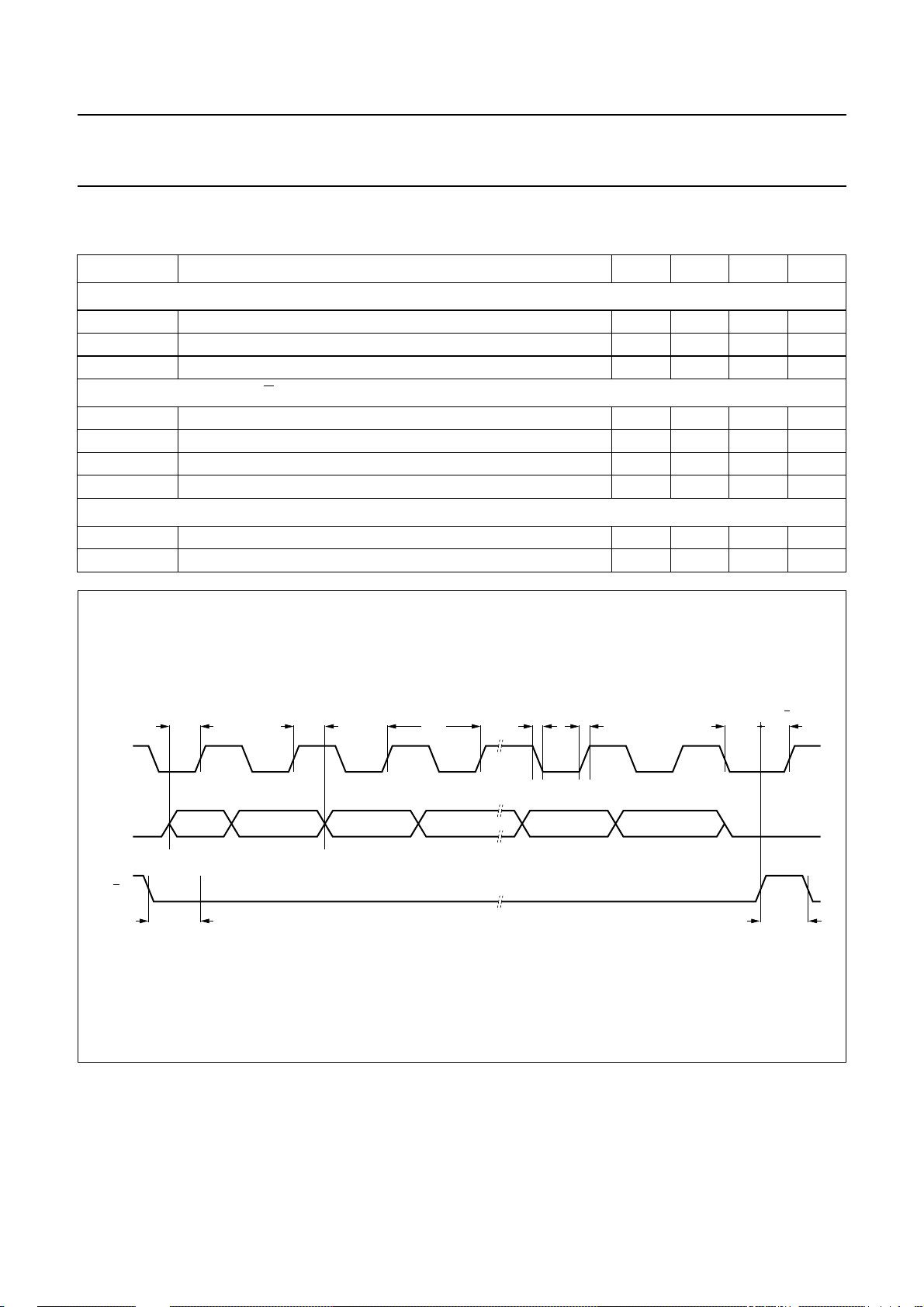
SERIAL TIMING CHARACTERISTICS
Initial parameter values: VCC= 2.6 V ±5%; T
SYMBOL PARAMETER MIN. TYP. MAX. UNIT
Serial programming clock: pin CLK
t
r
t
f
T
cy
rise time − 10 20 ns
fall time − 10 20 ns
clock cycle time 200 −−ns
Enable programming: pin E
t
su(E)
t
h(E)
t
W(E)
t
su(E)
delay to rising clock edge 200 −−ns
delay from last falling clock edge 100 −−ns
minimum inactive pulse width 4000 −−ns
enable set-up time to next clock edge 200 −−ns
Register serial input data: pin DATA
t
su(D)
t
h(D)
input data to clock set-up time 50 −−ns
input data to clock hold time 50 −−ns
= −30 to +70 °C; unless otherwise specified; see Fig.3.
amb
handbook, full pagewidth
CLK
DATA
E
t
SU;DAT
t
START
t
HD;DAT
MSB LSB ADDRESS
T
cy
t
t
f
r
Fig.3 Timing diagram 3-wire serial bus.
MGD565
t
ENDtSU;E
t
W(min)
2000 Feb 17 18
Page 19
This text is here in white to force landscape pages to be rotated correctly when browsing through the pdf in the Acrobat reader.This text is here in
_white to force landscape pages to be rotated correctly when browsing through the pdf in the Acrobat reader.This text is here inThis text is here in
white to force landscape pages tobe rotated correctly when browsing through the pdf in the Acrobat reader. white to forcelandscape pages to be ...
2000 Feb 17 19
handbook, full pagewidth
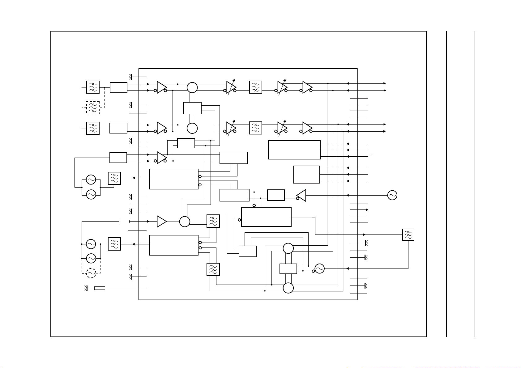
APPLICATION INFORMATION
Low power GSM/DCS/PCS multi-band
transceiver
Philips Semiconductors Objective specification
DCSRX
PCSRX
GSMRX
GSMTX
DCSTX
PCSTX
V
GSM/DCS/PCS
V
V
RFGND1
BALUN
RFGND2
V
CC(RF)
BALUN
RFLOGND
CC(RFLO)
BALUN
RFCPGND
CC(RFCP)
RFGND3
CC(TXCP)
TXCPGND
RFGND4
EXTRES
38
39
40
41
37
42
43
29
32
30
31
PHASE-FREQUENCY
24
DETECTOR AND
CHARGE PUMP
23
26
44
45
2
PHASE-FREQUENCY
1
DETECTOR AND
CHARGE PUMP
48
46
47
UAA3535HL
QUAD
1 : 1/2
×
7
×
×
3-WIRE BUS
MAIN
DIVIDER
REFERENCE
DIVIDER
1 : 6/7
PHASE-FREQUENCY
DETECTOR AND
CHARGE PUMP
CONTROL REGISTER
POWER
ENABLE
1 : 1/2
×
1 : 1/2
91 MHz GSM/DCS
78 MHz PCS
×
8
36
35
34
33
9
10
16
17
18
11
12
25
22
3
5
14
15
20
21
19
4
13
6
28
27
FCA075
IFCIA
IFCIB
IFCQA
IFCQB
DATA
CLK
E
RXON
TXON
SYNON
REFIN
TXIFA
TSTO
V
CC2(IF)
IFGND2
IFCPO
IFCPGND
V
CC(IFCP)
IFGND1
IFTUNE
V
CC1(IF)
SYNGND
V
CC(SYN)
IA
IB
QA
QB
13 MHz
VTCXO
UAA3535HL
Fig.4 Application diagram.
Page 20
Philips Semiconductors Objective specification
Low power GSM/DCS/PCS multi-band transceiver UAA3535HL
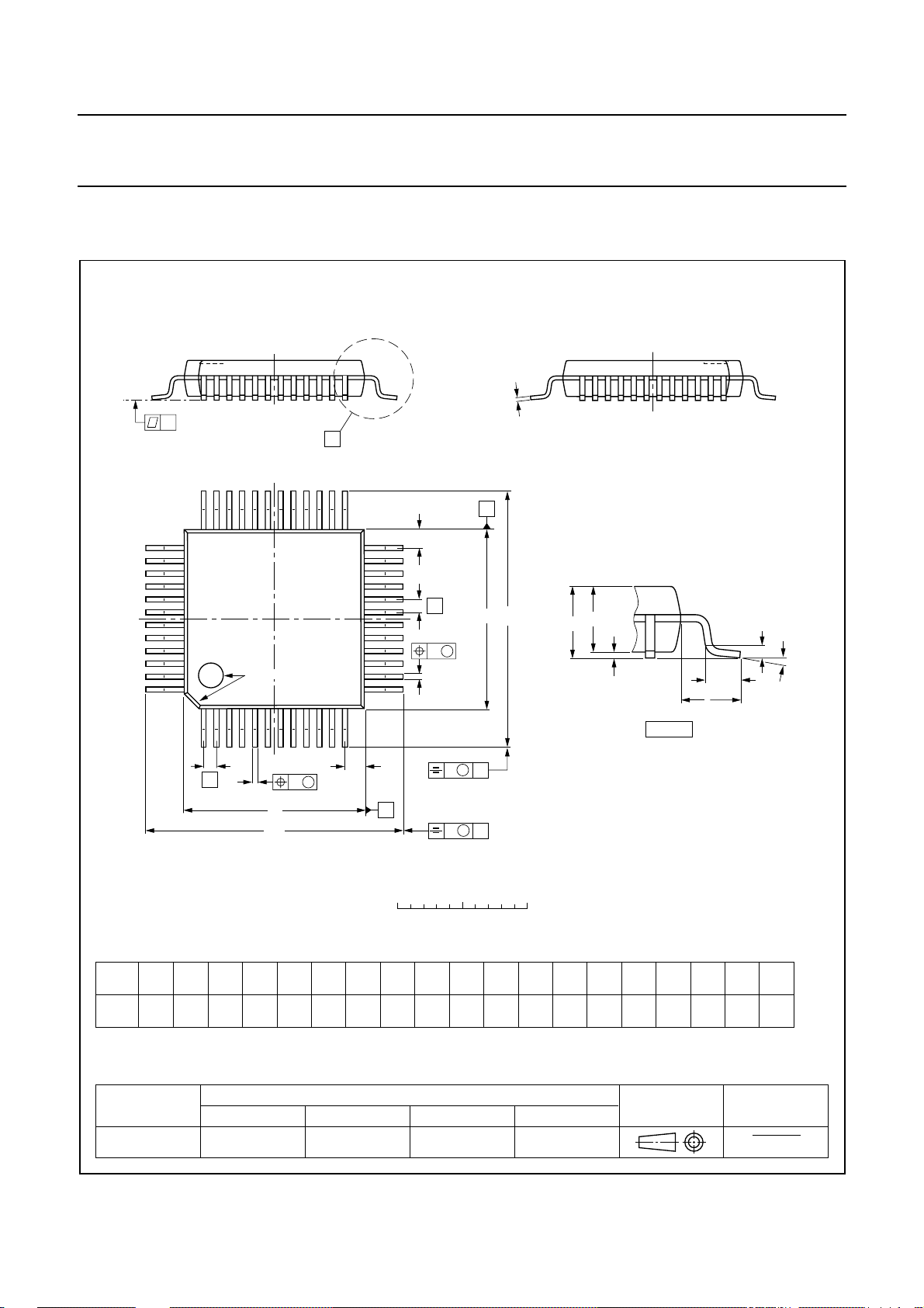
PACKAGE OUTLINE
LQFP48: plastic low profile quad flat package; 48 leads; body 7 x 7 x 1.4 mm
c
y
X
SOT313-2
36
37
pin 1 index
48
1
e
w M
b
p
D
H
D
DIMENSIONS (mm are the original dimensions)
mm
A
A1A2A3b
max.
0.20
1.60
0.05
1.45
1.35
0.25
cE
p
0.27
0.18
0.17
0.12
UNIT
25
Z
24
E
e
A
H
E
E
A
2
A
A
1
w M
b
p
13
12
Z
D
v M
A
detail X
B
v M
B
0 2.5 5 mm
scale
(1)
(1) (1)(1)
D
7.1
6.9
eH
H
D
7.1
6.9
0.5
9.15
8.85
E
9.15
8.85
LL
p
0.75
0.45
0.12 0.10.21.0
Z
0.95
0.55
L
L
D
(A )
3
p
Zywv θ
E
0.95
0.55
o
7
o
0
θ
Note
1. Plastic or metal protrusions of 0.25 mm maximum per side are not included.
OUTLINE
VERSION
IEC JEDEC EIAJ
REFERENCES
SOT313-2 MS-026136E05
2000 Feb 17 20
EUROPEAN
PROJECTION
ISSUE DATE
99-12-27
00-01-19
Page 21

Philips Semiconductors Objective specification
Low power GSM/DCS/PCS multi-band transceiver UAA3535HL
SOLDERING
Introduction to soldering surface mount packages
Thistext gives averybrief insight toacomplex technology.
A more in-depth account of soldering ICs can be found in
our
“Data Handbook IC26; Integrated Circuit Packages”
(document order number 9398 652 90011).
There is no soldering method that is ideal for all surface
mount IC packages.Wave solderingis not always suitable
for surface mount ICs, or for printed-circuit boards with
high population densities. In these situations reflow
soldering is often used.
Reflow soldering
Reflow soldering requires solder paste (a suspension of
fine solder particles, flux and binding agent) to be applied
tothe printed-circuit boardby screen printing,stencilling or
pressure-syringe dispensing before package placement.
Several methods exist for reflowing; for example,
infrared/convection heating in a conveyor type oven.
Throughput times (preheating, soldering and cooling) vary
between 100 and 200 seconds depending on heating
method.
Typical reflow peak temperatures range from
215 to 250 °C. The top-surface temperature of the
packages should preferable be kept below 230 °C.
Wave soldering
Conventional single wave soldering is not recommended
forsurface mount devices(SMDs)or printed-circuit boards
with a high component density, as solder bridging and
non-wetting can present major problems.
• For packages with leads on two sides and a pitch (e):
– larger than or equal to 1.27 mm, the footprint
longitudinal axis is preferred to be parallel to the
transport direction of the printed-circuit board;
– smaller than 1.27 mm, the footprint longitudinal axis
must be parallel to the transport direction of the
printed-circuit board.
The footprint must incorporate solder thieves at the
downstream end.
• Forpackages with leadsonfour sides, the footprintmust
be placedat a 45° angle to the transport direction of the
printed-circuit board. The footprint must incorporate
solder thieves downstream and at the side corners.
During placement and before soldering, the packagemust
be fixed with a droplet of adhesive. The adhesive can be
applied by screen printing, pin transfer or syringe
dispensing. The package can be soldered after the
adhesive is cured.
Typical dwell time is 4 seconds at 250 °C.
A mildly-activated flux will eliminate the need for removal
of corrosive residues in most applications.
Manual soldering
Fix the component by first soldering two
diagonally-opposite end leads. Use a low voltage (24 V or
less) soldering iron applied to the flat part of the lead.
Contact time must be limited to 10 seconds at up to
300 °C.
When using a dedicated tool, all other leads can be
soldered in one operation within 2 to 5 seconds between
270 and 320 °C.
To overcome these problems the double-wave soldering
method was specifically developed.
If wave soldering is used the following conditions must be
observed for optimal results:
• Use a double-wave soldering method comprising a
turbulent wavewith high upward pressure followed by a
smooth laminar wave.
2000 Feb 17 21
Page 22
Philips Semiconductors Objective specification
Low power GSM/DCS/PCS multi-band transceiver UAA3535HL
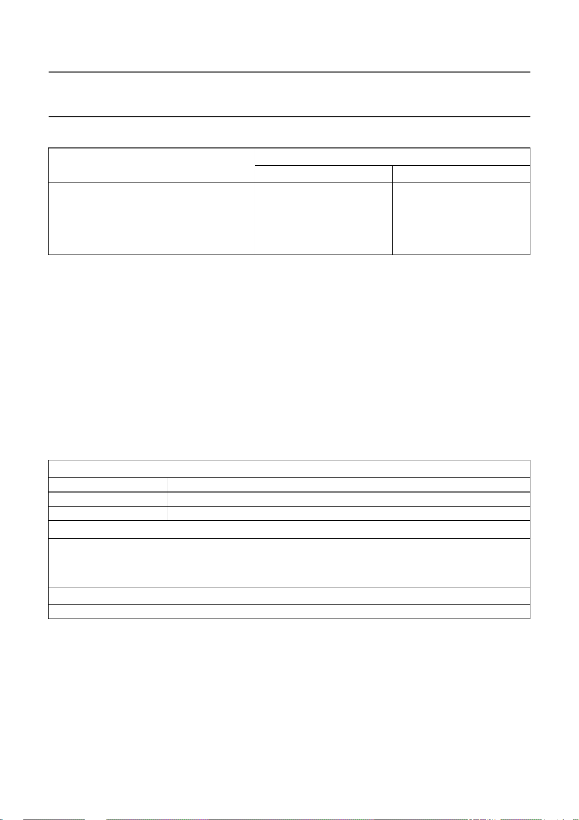
Suitability of surface mount IC packages for wave and reflow soldering methods
PACKAGE
WAVE REFLOW
(1)
BGA, SQFP not suitable suitable
SOLDERING METHOD
HLQFP, HSQFP, HSOP, HTQFP, HTSSOP, SMS not suitable
(3)
PLCC
, SO, SOJ suitable suitable
LQFP, QFP, TQFP not recommended
SSOP, TSSOP, VSO not recommended
(2)
(3)(4)
(5)
suitable
suitable
suitable
Notes
1. All surface mount (SMD) packages are moisture sensitive. Depending upon the moisture content, the maximum
temperature (with respect to time) and body size of the package, there is a risk that internal or external package
cracks may occur due to vaporization of the moisture in them (the so called popcorn effect). For details, refer to the
Drypack information in the
“Data Handbook IC26; Integrated Circuit Packages; Section: Packing Methods”
.
2. These packages are not suitable for wave soldering as a solder joint between the printed-circuit board and heatsink
(at bottom version) can not be achieved, and as solder may stick to the heatsink (on top version).
3. If wave soldering is considered, then the package must be placed at a 45° angle to the solder wave direction.
The package footprint must incorporate solder thieves downstream and at the side corners.
4. Wave soldering is only suitable for LQFP, TQFP and QFP packages with a pitch (e) equal to or larger than 0.8 mm;
it is definitely not suitable for packages with a pitch (e) equal to or smaller than 0.65 mm.
5. Wave soldering is onlysuitable for SSOP and TSSOP packages witha pitch (e) equal toor largerthan 0.65 mm; it is
definitely not suitable for packages with a pitch (e) equal to or smaller than 0.5 mm.
DEFINITIONS
Data sheet status
Objective specification This data sheet contains target or goal specifications for product development.
Preliminary specification This data sheet contains preliminary data; supplementary data may be published later.
Product specification This data sheet contains final product specifications.
Limiting values
Limiting values given are in accordance with the Absolute Maximum Rating System (IEC 134). Stress above one or
more of the limiting values may cause permanent damage to the device. These are stress ratings only and operation
of the device at these or at any other conditions above those given in the Characteristics sections of the specification
is not implied. Exposure to limiting values for extended periods may affect device reliability.
Application information
Where application information is given, it is advisory and does not form part of the specification.
LIFE SUPPORT APPLICATIONS
These products are not designed for use in life support appliances, devices, or systems where malfunction of these
products can reasonably be expected to result in personal injury. Philips customers using or selling these products for
use in such applications do so at their own risk and agree to fully indemnify Philips for any damages resulting from such
improper use or sale.
2000 Feb 17 22
Page 23

Philips Semiconductors Objective specification
Low power GSM/DCS/PCS multi-band transceiver UAA3535HL
NOTES
2000 Feb 17 23
Page 24

Philips Semiconductors – a w orldwide compan y
Argentina: see South America
Australia: 3 Figtree Drive, HOMEBUSH, NSW 2140,
Tel. +61 2 9704 8141, Fax. +61 2 9704 8139
Austria: Computerstr. 6, A-1101 WIEN, P.O. Box 213,
Tel. +43 1 60 101 1248, Fax. +43 1 60 101 1210
Belarus: Hotel Minsk Business Center, Bld. 3, r. 1211, Volodarski Str. 6,
220050 MINSK, Tel. +375 172 20 0733, Fax. +375 172 20 0773
Belgium: see The Netherlands
Brazil: see South America
Bulgaria: Philips Bulgaria Ltd., Energoproject, 15th floor,
51 James Bourchier Blvd., 1407 SOFIA,
Tel. +359 2 68 9211, Fax. +359 2 68 9102
Canada: PHILIPS SEMICONDUCTORS/COMPONENTS,
Tel. +1 800 234 7381, Fax. +1 800 943 0087
China/Hong Kong: 501 Hong Kong Industrial Technology Centre,
72 Tat Chee Avenue, Kowloon Tong, HONG KONG,
Tel. +852 2319 7888, Fax. +852 2319 7700
Colombia: see South America
Czech Republic: see Austria
Denmark: Sydhavnsgade 23, 1780 COPENHAGEN V,
Tel. +45 33 29 3333, Fax. +45 33 29 3905
Finland: Sinikalliontie 3, FIN-02630 ESPOO,
Tel. +358 9 615 800, Fax. +358 9 6158 0920
France: 51 Rue Carnot, BP317, 92156 SURESNES Cedex,
Tel. +33 1 4099 6161, Fax. +33 1 4099 6427
Germany: Hammerbrookstraße 69, D-20097 HAMBURG,
Tel. +49 40 2353 60, Fax. +49 40 2353 6300
Hungary: see Austria
India: Philips INDIA Ltd, Band Box Building, 2nd floor,
254-D, Dr. Annie Besant Road, Worli, MUMBAI 400 025,
Tel. +91 22 493 8541, Fax. +91 22 493 0966
Indonesia: PT Philips Development Corporation, Semiconductors Division,
Gedung Philips, Jl. Buncit Raya Kav.99-100, JAKARTA 12510,
Tel. +62 21 794 0040 ext. 2501, Fax. +62 21 794 0080
Ireland: Newstead, Clonskeagh, DUBLIN 14,
Tel. +353 1 7640 000, Fax. +353 1 7640 200
Israel: RAPAC Electronics, 7 Kehilat Saloniki St, PO Box 18053,
TEL AVIV 61180, Tel. +972 3 645 0444, Fax. +972 3 649 1007
Italy: PHILIPS SEMICONDUCTORS, Via Casati, 23 - 20052 MONZA (MI),
Tel. +39 039 203 6838, Fax +39 039 203 6800
Japan: Philips Bldg 13-37, Kohnan 2-chome, Minato-ku,
TOKYO 108-8507, Tel. +81 3 3740 5130, Fax. +81 3 3740 5057
Korea: Philips House, 260-199 Itaewon-dong, Yongsan-ku, SEOUL,
Tel. +82 2 709 1412, Fax. +82 2 709 1415
Malaysia: No. 76 Jalan Universiti, 46200 PETALING JAYA, SELANGOR,
Tel. +60 3 750 5214, Fax. +60 3 757 4880
Mexico: 5900 Gateway East, Suite 200, EL PASO, TEXAS 79905,
Tel. +9-5 800 234 7381, Fax +9-5 800 943 0087
Middle East: see Italy
Netherlands: Postbus 90050, 5600 PB EINDHOVEN, Bldg. VB,
Tel. +31 40 27 82785, Fax. +31 40 27 88399
New Zealand: 2 Wagener Place, C.P.O. Box 1041, AUCKLAND,
Tel. +64 9 849 4160, Fax. +64 9 849 7811
Norway: Box 1, Manglerud 0612, OSLO,
Tel. +47 22 74 8000, Fax. +47 22 74 8341
Pakistan: see Singapore
Philippines: Philips Semiconductors Philippines Inc.,
106 Valero St. Salcedo Village, P.O. Box 2108 MCC, MAKATI,
Metro MANILA, Tel. +63 2 816 6380, Fax. +63 2 817 3474
Poland: Al.Jerozolimskie 195 B, 02-222 WARSAW,
Tel. +48 22 5710 000, Fax. +48 22 5710 001
Portugal: see Spain
Romania: see Italy
Russia: Philips Russia, Ul. Usatcheva 35A, 119048 MOSCOW,
Tel. +7 095 755 6918, Fax. +7 095 755 6919
Singapore: Lorong 1, Toa Payoh, SINGAPORE 319762,
Tel. +65 350 2538, Fax. +65 251 6500
Slovakia: see Austria
Slovenia: see Italy
South Africa: S.A. PHILIPS Pty Ltd., 195-215 Main Road Martindale,
2092 JOHANNESBURG, P.O. Box 58088 Newville 2114,
Tel. +27 11 471 5401, Fax. +27 11 471 5398
South America: Al. Vicente Pinzon, 173, 6th floor,
04547-130 SÃO PAULO, SP, Brazil,
Tel. +55 11 821 2333, Fax. +55 11 821 2382
Spain: Balmes 22, 08007 BARCELONA,
Tel. +34 93 301 6312, Fax. +34 93 301 4107
Sweden: Kottbygatan 7, Akalla, S-16485 STOCKHOLM,
Tel. +46 8 5985 2000, Fax. +46 8 5985 2745
Switzerland: Allmendstrasse 140, CH-8027 ZÜRICH,
Tel. +41 1 488 2741 Fax. +41 1 488 3263
Taiwan: Philips Semiconductors, 6F, No. 96, Chien Kuo N. Rd., Sec. 1,
TAIPEI, Taiwan Tel. +886 2 2134 2886, Fax. +886 2 2134 2874
Thailand: PHILIPS ELECTRONICS (THAILAND) Ltd.,
209/2 Sanpavuth-Bangna Road Prakanong, BANGKOK 10260,
Tel. +66 2 745 4090, Fax. +66 2 398 0793
Turkey: Yukari Dudullu, Org. San. Blg., 2.Cad. Nr. 28 81260 Umraniye,
ISTANBUL, Tel. +90 216 522 1500, Fax. +90 216 522 1813
Ukraine: PHILIPS UKRAINE, 4 Patrice Lumumba str., Building B, Floor 7,
252042 KIEV, Tel. +380 44 264 2776, Fax. +380 44 268 0461
United Kingdom: Philips Semiconductors Ltd., 276 Bath Road, Hayes,
MIDDLESEX UB3 5BX, Tel. +44 208 730 5000, Fax. +44 208 754 8421
United States: 811 East Arques Avenue, SUNNYVALE, CA 94088-3409,
Tel. +1 800 234 7381, Fax. +1 800 943 0087
Uruguay: see South America
Vietnam: see Singapore
Yugoslavia: PHILIPS, Trg N. Pasica 5/v, 11000 BEOGRAD,
Tel. +381 11 3341 299, Fax.+381 11 3342 553
For all other countries apply to: Philips Semiconductors,
International Marketing & Sales Communications, Building BE-p, P.O. Box 218,
5600 MD EINDHOVEN, The Netherlands, Fax. +31 40 27 24825
© Philips Electronics N.V. SCA
All rights are reserved. Reproduction in whole or in part is prohibited without the prior written consent of the copyright owner.
The information presented in this document does not form part of any quotation or contract, is believed to be accurate and reliable and may be changed
without notice. No liability will be accepted by the publisher for any consequence of its use. Publication thereof does not convey nor imply any license
under patent- or other industrial or intellectual property rights.
2000
Internet: http://www.semiconductors.philips.com
69
Printed in The Netherlands 403506/01/pp24 Date of release:2000 Feb 17 Document order number: 9397 750 06172
 Loading...