

Page 1
Adronic Components GmbH
Phase Control Circuit for Industrial Applications
Description
The UAA145 is a bipolar integrated circuit, designed to
provide phase control for industrial applications. It
permits the number of components in thyristor drive
circuits to be drastically reduced. The versatility of the
device is further enhanced by the provision of a large
number of pins giving access to internal circuit points.
UAA145
Features
D
Separate pulse output synchronized by mains
half wave
D
Output pulse-width is freely adjustable
D
Phase angle variable from >0° to <180°
D
High-impedance phase shift input
D
Less than 3° pulse symmetry between two half-cycles
or phase of different integrated circuits
D
Output pulse blocking
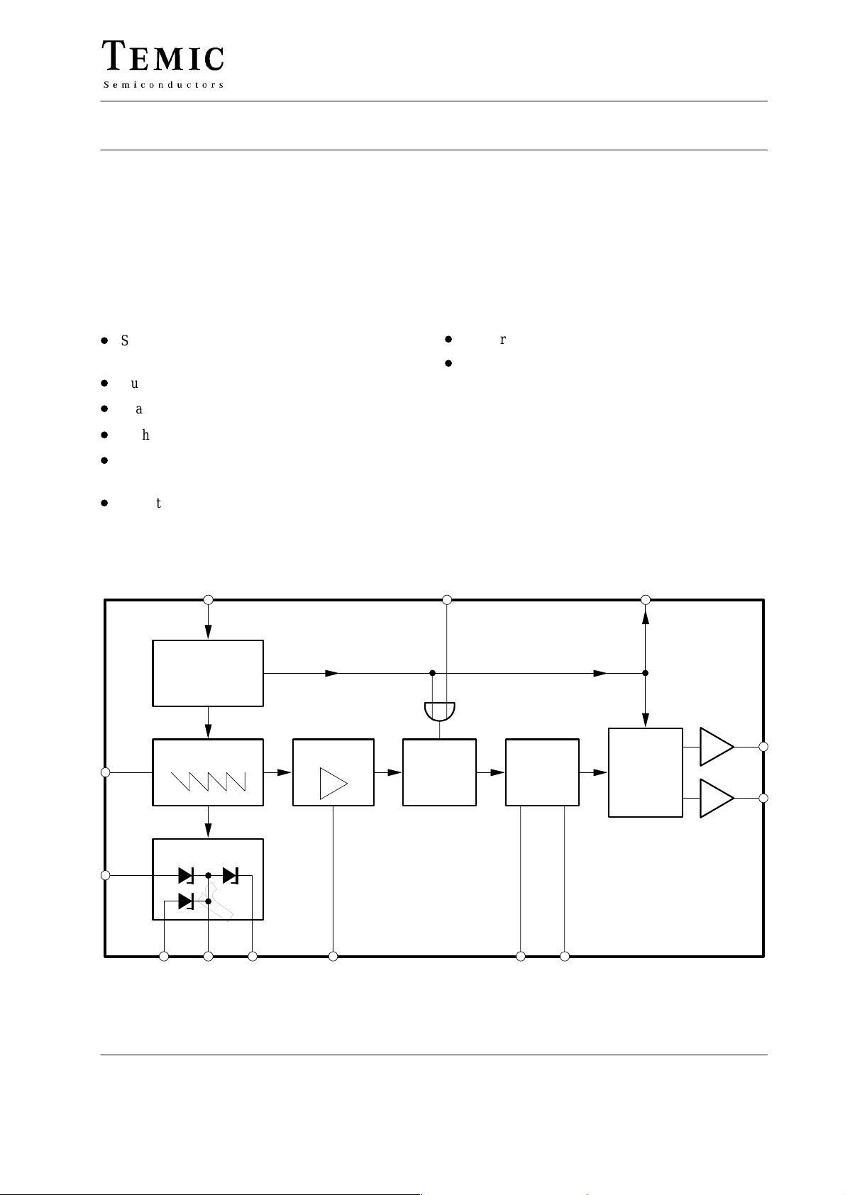
Block Diagram
Voltage
synchronisation
Comparator
7
–V
15
Ramp generator
Supply
Ref
Applications
D
Industrial power control
D
Silicon controlled rectifier
Package: DIP16 (special case)
Pulse inhibit6916
Memory
S
R
Puls
generator
Channel
selection
Pos. / Neg.
half wave
PHW
10
14
NHW
+15 –15
13 3 1 8
95 11298
TELEFUNKEN Semiconductors
Rev . A1, 29-May-96
8 211
PHW = Positive half wave
NHW = Negative half wave
Figure 1. Block diagram
1 (11)
Page 2
Adronic Components GmbH
UAA145
General Description
The operation of the circuit is best explained with the help
of the block diagram shown in figure 1. It comprises a
synchronizing stage, ramp generator, voltage
com-parator, pulse generator, channel selecting stage and
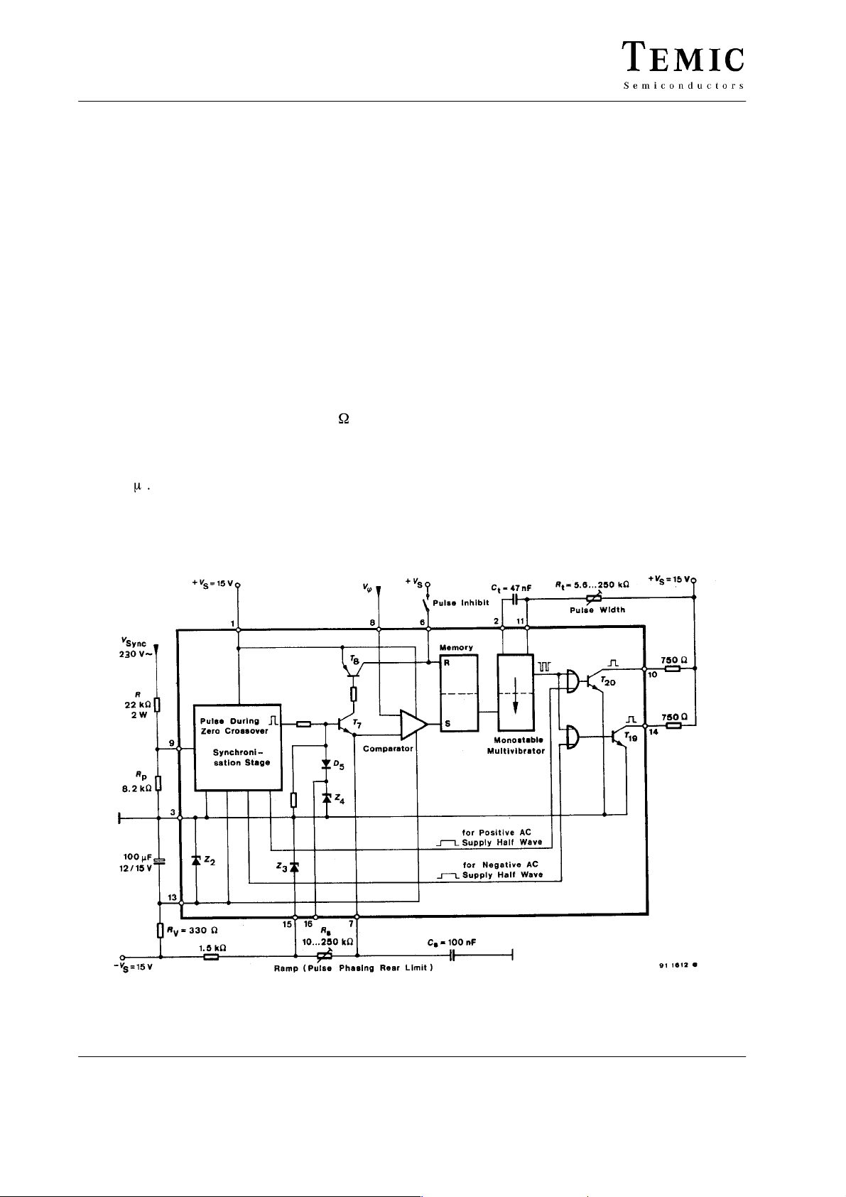
two output amplifiers. The circuit diagram in figure 2 also
shows the external components and terminal connections
necessary for operation of the circuit.
As can be seen from figure 2, the circuit requires two
supply rails i.e. a +15 V and a –15 V. The positive voltage
is applied directly to Pin 1, while an external series
resistor in each line is used to connect the negative
voltage Pin 13 and Pin 15. In the following circuit
description each section of the block diagrams is
discussed separately.
Synchronization Stage
Pin 9 is connected, via a voltage divider (22 kW and Rp),
to the ac line (sync. signal source). A pulse is generated
during each zero crossover of the sync. input. The pulse
duration depends on the resistance R
50 to 100 ms. (figure 2).
In addition to providing zero voltage switching pulses this
section of the circuit generates blocking signals for use in
the channel selecting stage.
and has a value of
p
Ramp Generator
Transistor T7 amplifies the zero-crossover switching
pulses. During the sync process capacitor C
charged to the operating voltage of reference diode Z
i.e., to approximately 8.5 V, the charging time being
always less than the duration of the sync pulse. The
capacitor discharges via resistor R
half-cycle. The discharge voltage is of the same
magnitude as the charge voltage, and is determined by Z
To ensure an approximately linear ramp waveform, the
voltage is allowed to decay up to ca. 0.7 C
Z-diodes Z
characteristics, the timing of the ramp zero crossover
point in relation to that of the sync. pulse is constant, and
consequently the pulse phasing rear limit is also very
stable.
and Z4have the same temperature
3
at Pin 7 is
S
during each
S
. Because
sRs
,
4
.
3
2 (11)
Figure 2. Block diagram and basic circuit
TELEFUNKEN Semiconductors
Rev . A1, 29-May-96
Page 3
Adronic Components GmbH
UAA145
Comparator (Differential Amplifier)
and Memory
In the (voltage) comparator stage, the ramp voltage is
compared with the shift voltage V
comparator switches whenever the instantaneous ramp
voltage is the same as the shift voltage (corresponding to
the desired phase angle), thereby causing the memory to
be set, i.e. the integrated thyristor in memory is to be
turned on. The time delay between the signal input and
the comparator output signal is proportional to the
required phase angle. Design of the circuit is such that the
memory content is reset only during the instant of zero
crossover, the reset signal always overriding the set
signal. This effectively prevents the generation of
additional output pulses and causes any pulse already
started to be immediately inhibited on application of an
inhibit signal to Pin 6. The memory content can also be
reset via Pin 6. Thus the memory ensures that any noise
(negative voltage transients) superimposed on the shift
signal at Pin 8 cannot give rise to the generation of
multiple pulses during the half-cycle.
applied to Pin 8. The
ö
Pulse Generator
(Monostable Multivibrator)
pulse can be monitored by means of an oscilloscope applied to Pin 6. The Pin 11 pulse waveform is that at C
the waveforms at Pin 10 and Pin 11 are those of the output
pulses.
, and
t
The memory setting pulse also triggers a monostable
stage. The duration of the pulse produced by the mono-
and R
stable is determined by C
Pin 11.
t
, connected to Pin 2 and
t
Channel Selection and Output
Amplifier
A pulse is produced at either output Pin 10 or Pin 14 if
transistor T
derived from the pulse generator are applied to the output
transistors via OR gates controlled by the half-cycle
signals derived from the sync stage. During the positive
half-cycle no signal is applied from the sync stage to T
so that an output pulse is produced at Pin 14. The same is
valid for Pin 10 during the negative half-cycle.
or T19respectively is cut-off. The pulses
20
19
Pulse Diagram
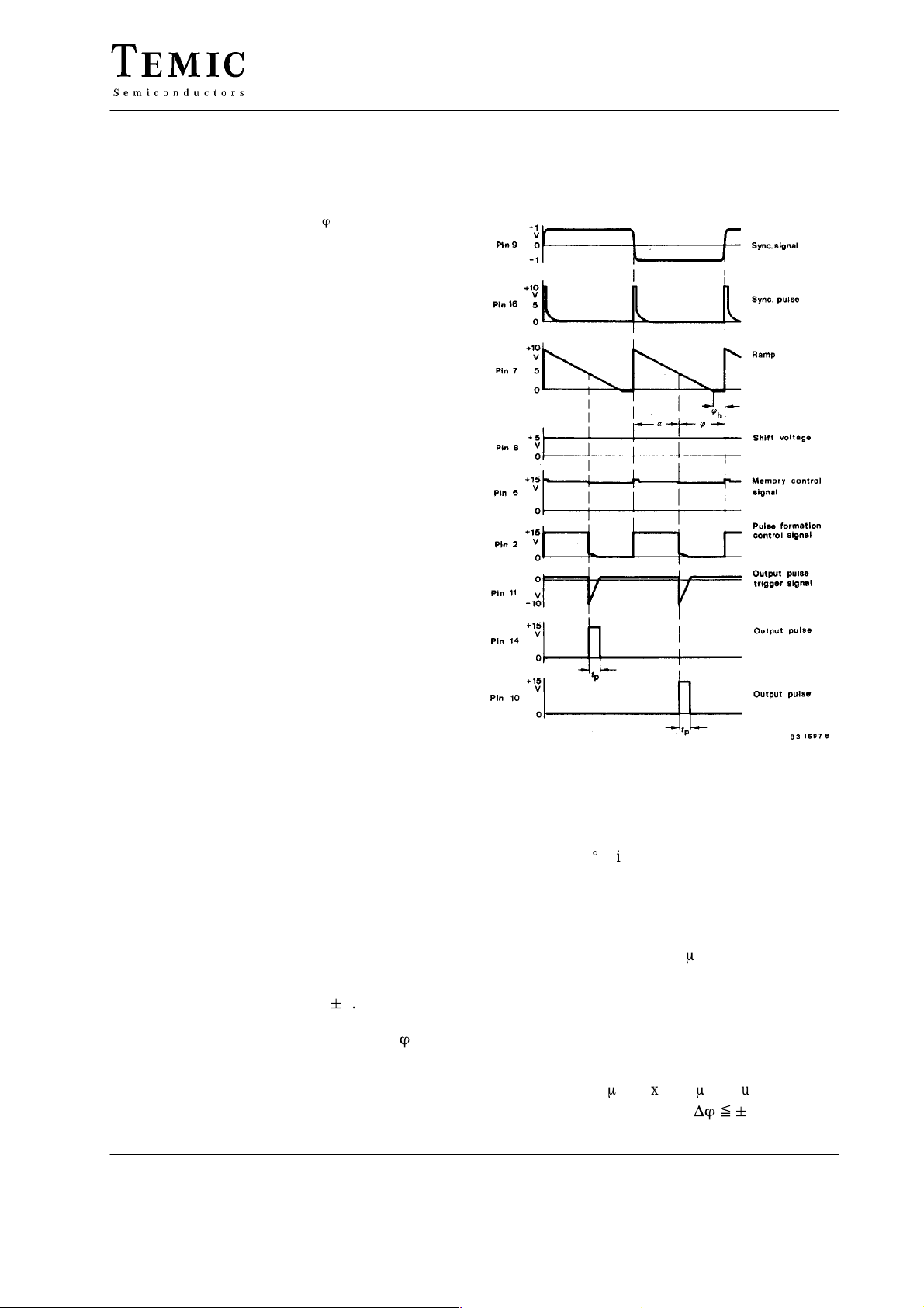
Figure 3 shows the pulse voltage waveforms measured at
various points of the circuit, all signals being time
referenced to the sync signal shown at the top. The input
circuit limits any signal applied to "0.8 V at Pin 9. The
sync pulse can be measured at Pin 16, whereas the ramp
waveform and the pulse phasing rear limit (
Pin 7. The time relationship between the shift voltage applied to Pin 8 and the ramp waveform is indicated by
dotted lines. A pulse trigger signal is produced whenever
the ramp crosses the shift level. The memory control
) are at
ö
h
Figure 3. Pulse diagram
Influence of External Components,
Syncronization Time
An ideal 0 to 180_ shift range and perfect half-cycle pulse
timing symmetry are attained, if the sync pulse duration
is kept short. However, there is a lower pulse duration
limit, which is governed by the time required to charge
capacitor C
As can be seen, it takes about 35 ms to charge C
time can be altered by adjustment of R
between R
The ratio of R and R
sync pulse, t
for sync pulse of 230 V∼. The lower the sync voltage,
longer is the sync pulse.
A minimum of 50 ms (max. 200 ms) input sync pulse is
required for a pulse symmetry of Döx"
(figure 5).
s
. The sync
s
, the relationship
and the sync time being shown in figure 6.
p
sync
determines the width of internal
p
, at Pin 16. The pulse shape is valid only
p
3°.
TELEFUNKEN Semiconductors
Rev . A1, 29-May-96
3 (11)
Page 4
Adronic Components GmbH
UAA145
95 11299
v
sync
t
v
10,14
v
14
v
10
ö
h
t
ö
95 10105
ö
v
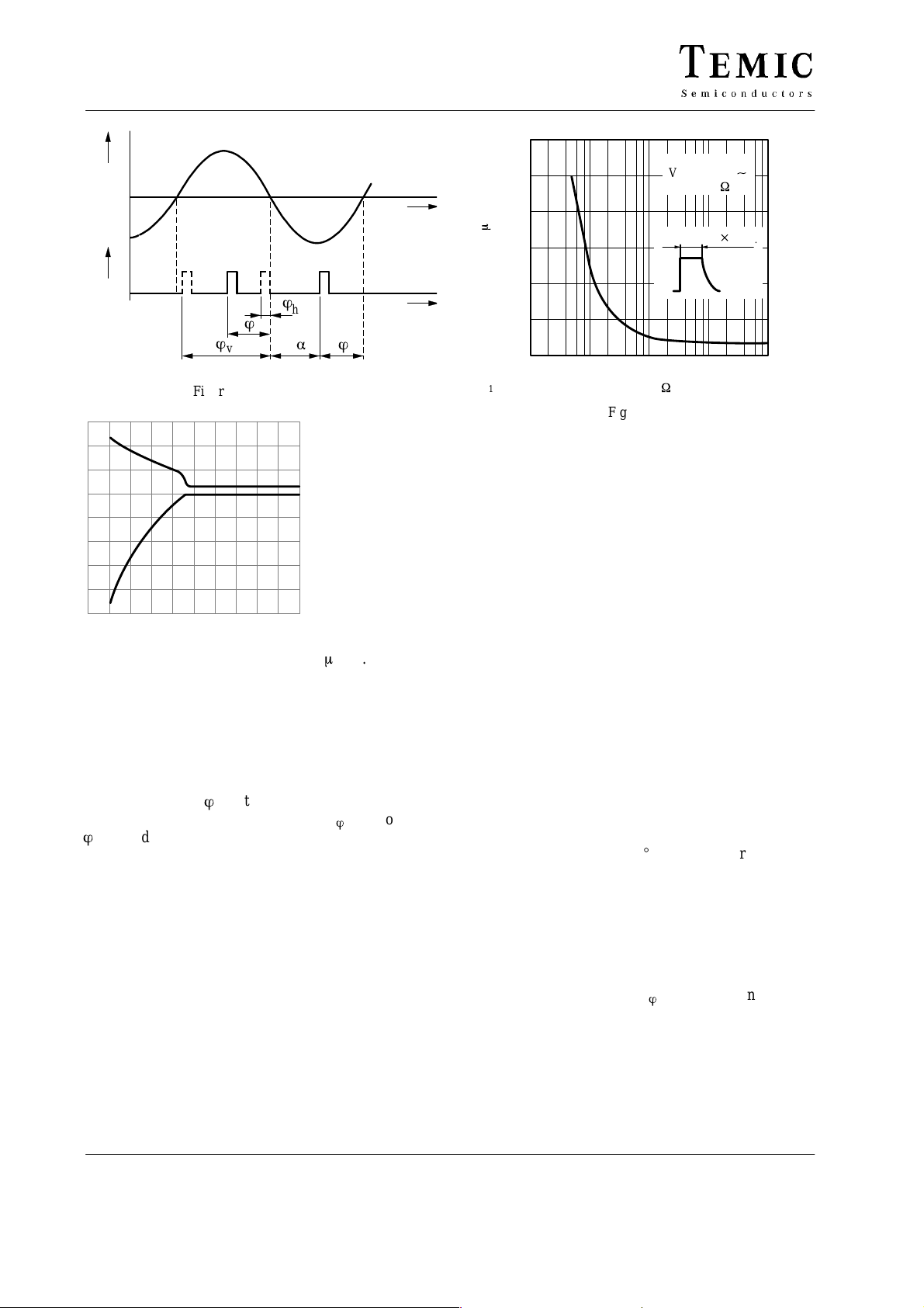
Figure 4. Pulse phasing
Figure 5. Charging time 10
a
P7 20mA/div.
–0mA
P
2V/div.
7
–0V
m
s/div.
ö
Pulse Phasing Limits
The pulse phasing front limit is determined by limiting
the maximum shift voltage applied to Pin 8 which is thus
adjustable by external circuitry. This can be done by
connecting a Z-diode between Pin 8 and Pin 3. The pulse
phasing rear limit,
output pulses when the shift voltage V
coincides with the zero crossover point of the ramp, it
ö
h
can be adjusted by variation of the time constant C
, is the residual phase angle of the
ö
h
is zero. Since
ö
sRs
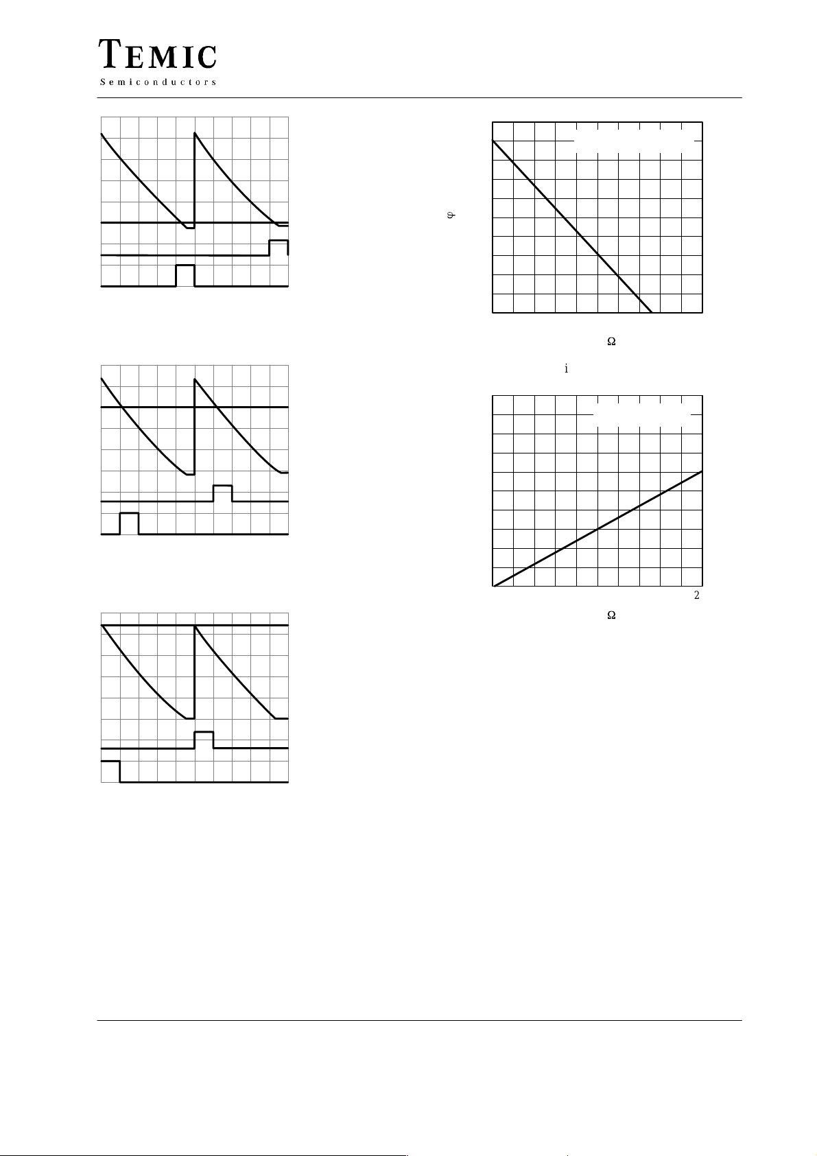
(figure 14). Figure 10 shows the pulse phasing rear limit
plotted as a function of R
.
s
Pulse Blocking
The output pulses can be blocked via Pin 6, the memory
content being erased whenever Pin 6 is connected to +V
(Pin 1). This effectively de-activates the pulse generator;
any output pulse in the process of generation is interrupted.
Pulse blocking can be accomplished either via relay
contacts or a PNP switching transistor (figure 14).
600
Sync. Time
V
=230V
500
400
m
300
Sync.
t ( s )
200
100
95 10106
Sync.
R=22k
0
0.1 1 10 100
RP ( kW )
Figure 6.
W
2 t
X
Sync.
Pin16
Output Pulse Width
The output pulse width can be varied by adjustment of R
and C
.In figure 11 pulse width is shown plotted as a func-
t
tion of R
for Ct= 50 nF.
t
The output pulse always finishes at zero crossover. This
means that if there is a minimum pulse width requirement
(for example, when the load is inductive) provision must
be made for a corresponding pulse phasing rear limit. The
output stages are arranged so that the transistors are cut
off when a pulse is produced. Consequently, the thyristor
trigger pulse current flows via the external load resistors,
this current being passed by the transistors during the
period when no output pulse is produced. During this
period the output voltage drops to the transistor saturation
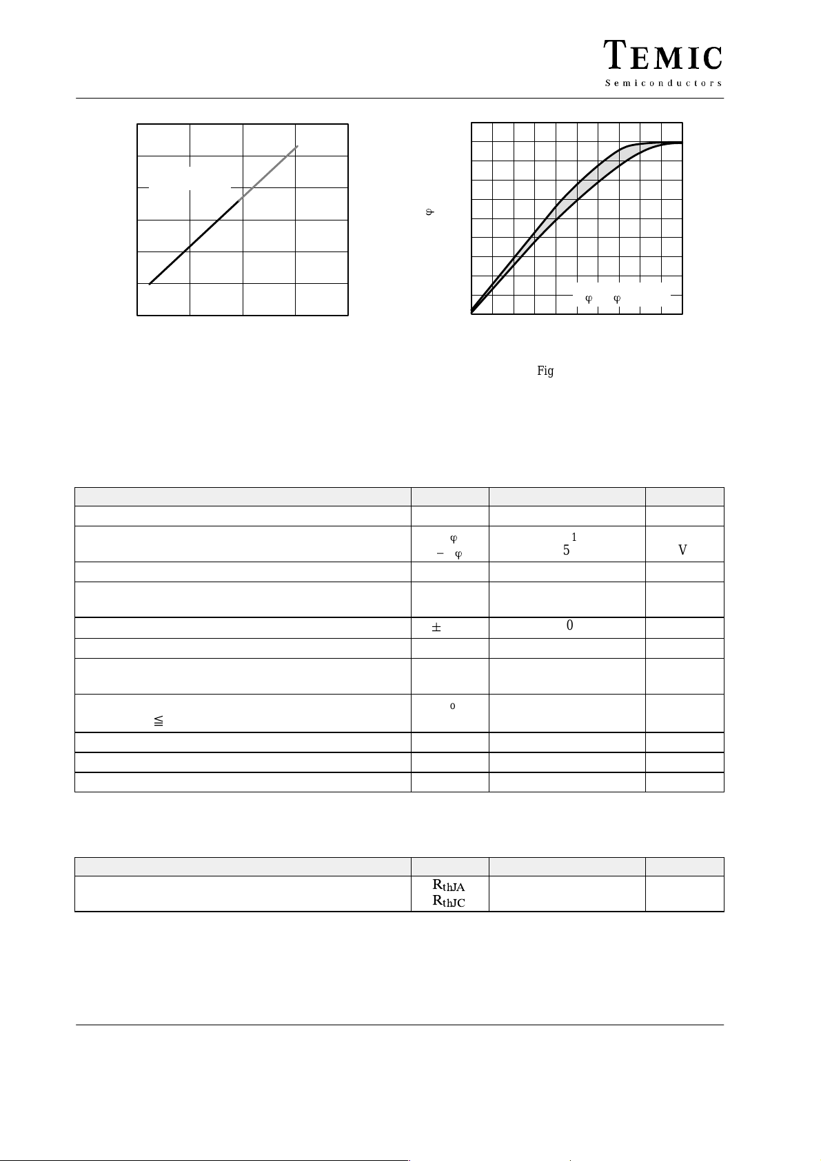
level and is therefore load dependent. Figure 12 shows
the relationship between saturation voltage and load
current.
Shift Characteristic
In figure 13 the angle of phase shift is shown plotted as a
function of the voltage applied to Pin 8 for a pulse phasing
rear limit of approximately 0_. Because the ramp waveform is a part of the exponential function, the shift curve
is also exponential.
The limitation of the shift voltage to approximately 8.5 V
is due to the internal Z-diode Z
spread of 7 to 9 V.
S
The waveforms in figures 7 to 9 show the output pulse
phase shift as a function of V
oscillograms, the instants at which pulses are released
coincide with the intersections of the ramp and the shift
voltage.
, which has a voltage
4
. It can be seen from the
ö
1000
t
4 (11)
TELEFUNKEN Semiconductors
Rev . A1, 29-May-96
Page 5
Adronic Components GmbH
UAA145
95 10107
Figure 7. Output pulses phase shift 2 ms/div
95 10108
Figure 8. Output pulses phase shift 2 ms/div
P7Ramp 2V/div.
–0mA
P
Ref. Voltage 2V/div.
8
0V
V
20V/div.
14
0V
V
20V/div.
10
–0V
P8 Ref. Voltage 2V/div.
P
Ramp 2V/div.
7
0V
20V/div.
V
14
0V
V
20V/div.
10
0V
( )°
h
ö
95 10295
p
t ( ms )
95 10296
200
160
120
80
40
0
0 40 80 120 160
Pulse Phasing Rear Limit
V
=0, Cs=100nF
B
Rs ( kW )
Figure 10.
10
8
6
4
2
0
0 40 80 120 160
Output Pulse Width
Rt ( kW )
C
t
200
=50nF
200
95 10294
Figure 9. Output pulses phase shift 2 ms/div
TELEFUNKEN Semiconductors
Rev . A1, 29-May-96
P8 Ref. Voltage 2V/div.
P
Ramp 2V/div.
7
0V
20V/div.
V
14
0V
V
20V/div.
10
0V
Figure 11.
5 (11)
Page 6
Adronic Components GmbH
UAA145
0.6
0.5
Saturation
Output Voltages
0.4
14
10
V , V ( V )
95 10298
0.3
0.2
0.1
0
0102030
I10, I14 ( mA )
Figure 12.
40
ö
95 10297
Absolute Maximum Ratings
Reference point Pin 3, T
Positive supply voltage Pin 1 V
Shift voltage Pin 8 V
Reverse voltage, control input Pin 11 –V
Negative supply current Pin 13
Synchronization current Pin 9
Control input pulse current Pin 11 I
Output currents Pin 10
Total power dissipation
Tamb x 70°C
Junction temperature T
Ambient temperature range T
Storage temperature range T
= 25°C, unless otherwise specified
amb
Parameters Symbol Value Unit
Pin 15
"
Pin14
200
160
°( )
120
80
40
0
02468
S
ö
V
ö
-
IR
–I
S
Shift Characteristics
ö
h
( V )
V
8
Figure 13.
18 V
V
S1
5
15 V
25
5
I
sync
I
O
I
20 mA
3 mA
20
20
P
amb
tot
j
stg
550 mW
125 °C
–25 to +70 °C
–25 to +125 °C
ö
=0, =f (V8 )
10
V
V
mA
mA
Thermal Resistance
Parameters Symbol Value Unit
Junction ambient
Junction case
6 (11)
R
R
thJA
thJC
100
K/W
35
TELEFUNKEN Semiconductors
Rev . A1, 29-May-96
Page 7
Adronic Components GmbH
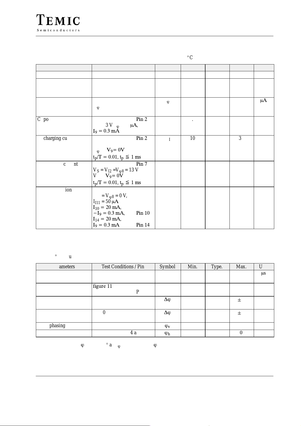
DC Characteristics
V
= 13 to 16 V, –I
S
1
Parameters Test Conditions / Pin Symbol Min. Typ. Max. Unit
Positive supply current VS= 16 V Pin 1 I
Voltage limitation –I
Input current VS = 16 V, Pin 8
Ct-potential shift current VS = VI2 =13 V,
Ct-charging current VS = 13 V,
CS-charging current
Output saturation voltage VS = VI2 =16 V,
= 15 mA, reference point Pin 3, figure 2, T
S13
= 15 mA Pin 13
S13
= 3.5 mA Pin 15
–I
S15
= 13 V, V9 = 0V Pin 16
V
S
= 13 V,
V
8
ö
= 0V, I9 = 0.3 mA
V
7
= 3 V, I
V
I7
I
ö
= 5
8
mA,
=VI7 = 0 V
V
I2
=
V
8
ö
x
= VI2 =V
V
S
=
V
I7
x
= V
V
I7
ö
= 50
I
I11
=2
10
=2
14
=0.3
=0.3
I
I
= 13 V
8
ö
= 0 V,
8
mA
–V
–V
V
V
V
= 25_C, unless otherwise specified
amb
S
Z4
I
ö
I
I
–I
–I
Osat
Osat
Z2
Z3
I
I
12 30 mA
7.0
7.0
7.0
4.5 mA
10 30 mA
20 62 mA
0.3
0.3
UAA145
9.0
9.0
9.0
10
1.0
1.0
V
mA
V
AC Characteristics
T
= 25_C, figures 2, 4 and 14
amb
Parameters Test Conditions / Pin Symbol Min. Type. Max. Unit
Rise time Pin 10
Pin 14
Pulse width
Pin 10
Pin 14
Pulse phasing difference
f = 50 Hz
for two half-waves
Inter lC phasing
f = 50 Hz
difference
Pulse phasing front limit f = 50 Hz, figure 4
Pulse phasing rear limit f = 50 Hz, figures 4 and 10
Angle of current flow ö = 0 to 177° at V
= 0.2 to 7.5 V,
8
ö
TELEFUNKEN Semiconductors
Rev . A1, 29-May-96
t
r
t
p
t
p
0.1
0.1
Dö
Dö
ö
ö
177 °
öh = 0°, figures 4 and 13
"
"
0.5
0.5
4
4
m
ms
3
3
°
°
°
7 (11)
Page 8
Adronic Components GmbH
UAA145
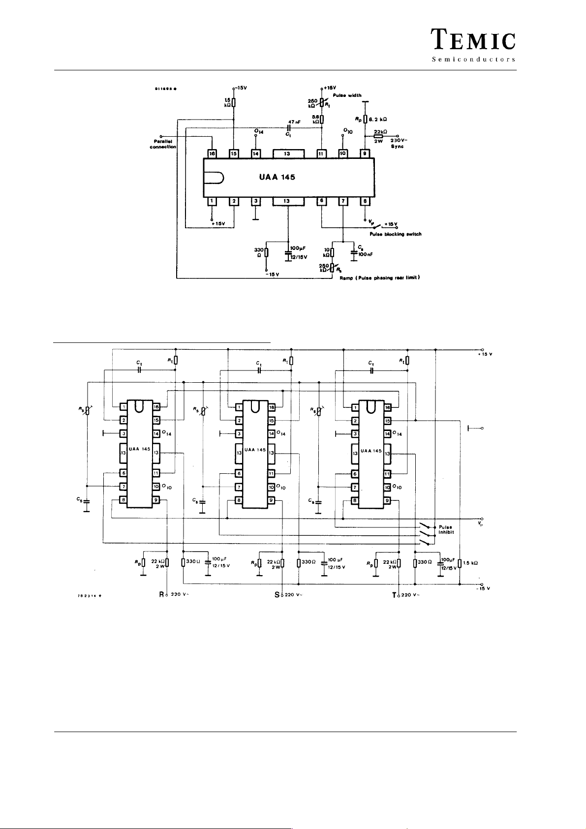
Figure 14. Test circuit for ac characteristics
Applications
Parallel connection for three-phase current applications
Figure 15. Parallel connection for three-phase current applications. For polyphase operation connect all Pins 15 and Pins 16.
To ensure good pulse phasing symmetry as well as
identical shift characteristics in three-phase applications,
when three devices are employed, two parallel
connection pins (figure 15) are provided on each device.
Besides the supply pins, the input pins 15 and 16 are to be
paralleled. If this is done, then all the Z
connected in parallel so that the reference voltage
8 (11)
and Z3diodes are
4
effective for all three devices becomes that of the Z-diode
with the lowest operating voltage. In this way all the C
capacitors are charged and discharged to the same voltage
levels. By symmetrical adjustment of the time constants
with resistors R
identical shift characteristics are attained.
, good pulse phasing symmetry and
S
TELEFUNKEN Semiconductors
Rev . A1, 29-May-96
S
Page 9
Adronic Components GmbH
UAA145
TELEFUNKEN Semiconductors
Rev . A1, 29-May-96
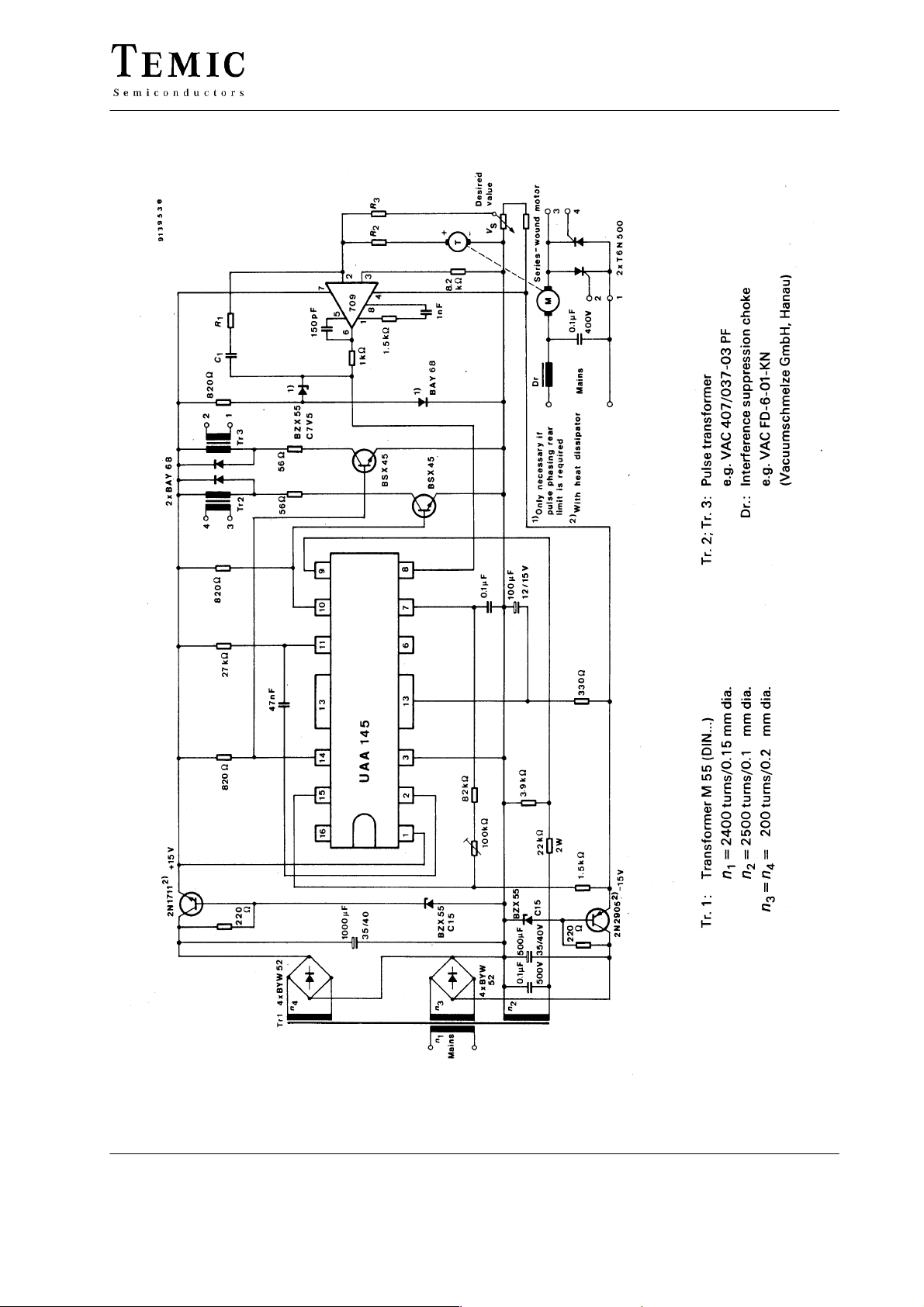
Figure 16. Speed control with tacho-generator
9 (11)
Page 10
Adronic Components GmbH
UAA145
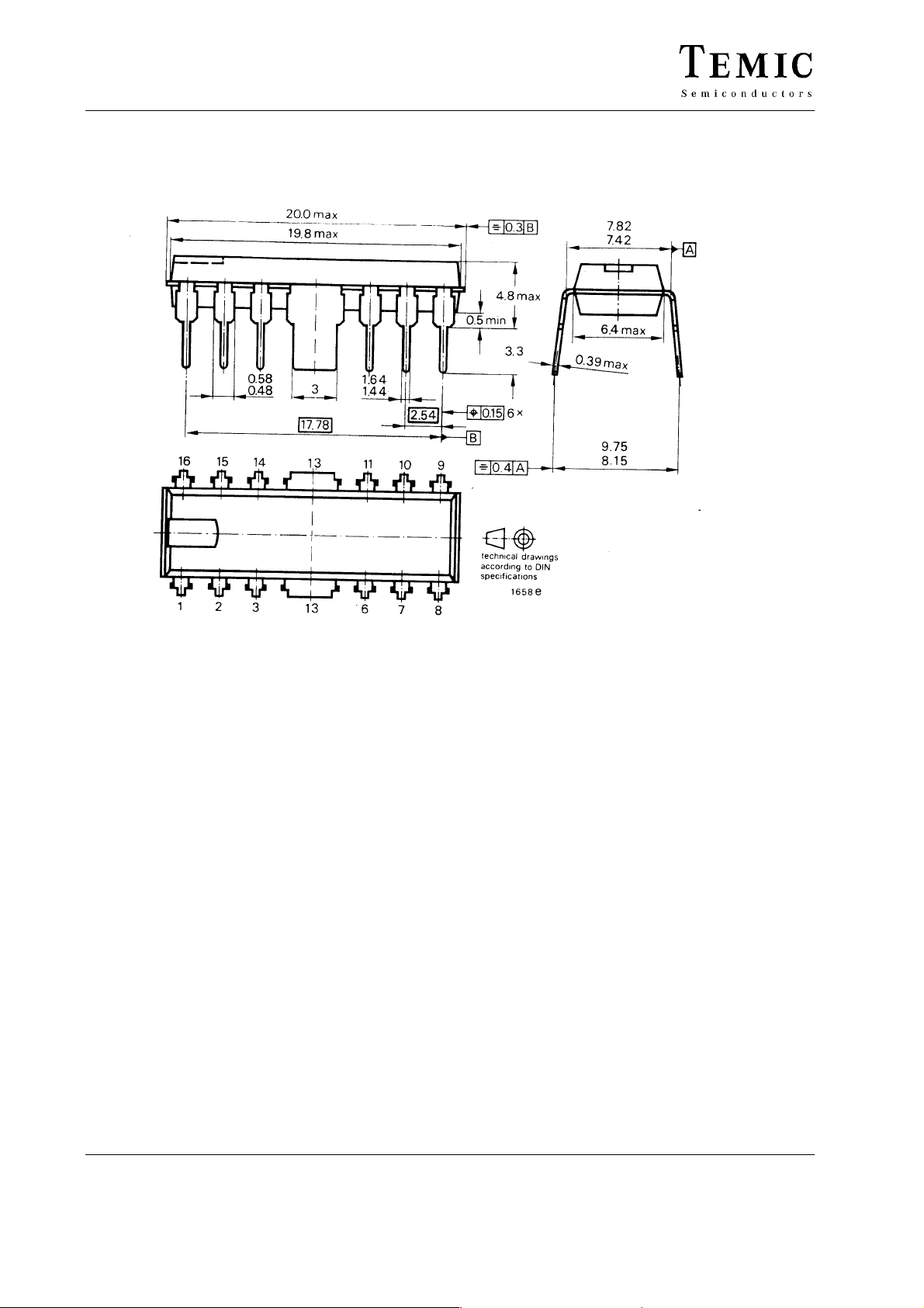
Dimensions in mm
Case:
DIP 16
(Special case)
10 (11)
TELEFUNKEN Semiconductors
Rev . A1, 29-May-96
Page 11

Adronic Components GmbH
UAA145
Ozone Depleting Substances Policy Statement
It is the policy of TEMIC TELEFUNKEN microelectronic GmbH to
1. Meet all present and future national and international statutory requirements.
2. Regularly and continuously improve the performance of our products, processes, distribution and operating systems
with respect to their impact on the health and safety of our employees and the public, as well as their impact on
the environment.
It is particular concern to control or eliminate releases of those substances into the atmosphere which are known as
ozone depleting substances (ODSs).
The Montreal Protocol ( 1987) and its London Amendments (1990) intend to severely restrict the use of ODSs and
forbid their use within the next ten years. Various national and international initiatives are pressing for an earlier ban
on these substances.
TEMIC TELEFUNKEN microelectronic GmbH semiconductor division has been able to use its policy of
continuous improvements to eliminate the use of ODSs listed in the following documents.
1. Annex A, B and list of transitional substances of the Montreal Protocol and the London Amendments respectively
2. Class I and II ozone depleting substances in the Clean Air Act Amendments of 1990 by the Environmental
Protection Agency (EPA) in the USA
3. Council Decision 88/540/EEC and 91/690/EEC Annex A, B and C (transitional substances) respectively .
TEMIC can certify that our semiconductors are not manufactured with ozone depleting substances and do not contain
such substances.
We reserve the right to make changes to improve technical design and may do so without further notice.
Parameters can vary in different applications. All operating parameters must be validated for each customer
application by the customer. Should the buyer use TEMIC products for any unintended or unauthorized
application, the buyer shall indemnify TEMIC against all claims, costs, damages, and expenses, arising out of,
directly or indirectly, any claim of personal damage, injury or death associated with such unintended or
unauthorized use.
TEMIC TELEFUNKEN microelectronic GmbH, P.O.B. 3535, D-74025 Heilbronn, Germany
TELEFUNKEN Semiconductors
Rev . A1, 29-May-96
Telephone: 49 (0)7131 67 2831, Fax number: 49 (0)7131 67 2423
11 (11)
 Loading...