

Page 1
UAC 3552A
Universal Serial Bus
DAC
Edition Nov. 9, 1999
6251-487-1PD
PRELIMINARY DATA SHEET
MICRONAS
MICRONAS
Page 2

UAC 3552A PRELIMINARY DATA SHEET
Contents
Page Section Title
4 1. Introduction
5 1.1. Features
6 2. Functional Description
6 2.1. Hardware
6 2.1.1. USB Interface
6 2.1.1.1. Transceiver
6 2.1.1.2. Interface Engine
6 2.1.1.3. Microcontroller
6 2.1.2. Audio Control Interface
6 2.1.3. Audio Streaming Interface
6 2.1.4. Audio Processing Unit
6 2.1.5. Analog Back-end
7 2.1.5.1. DAC
8 2.1.5.2. Analog Low-pass
8 2.1.5.3. Postfilter Op Amps
8 2.1.5.4. Input Mixer
9 2.1.5.5. Analog Volume Control
9 2.1.5.6. Line-out/Headphone Amplifier
9 2.1.6. General Purpose I/O
10 2.1.7. Special I/O
10 2.1.7.1. SOF (Start of Frame)
10 2.1.7.2. AUXEN
10 2.1.7.3. SUSPEND
10 2.1.8. Clock System
10 2.2. Software
10 2.2.1. USB Microcontroller Software
10 2.2.1.1. Chapter 9 Functions
10 2.2.1.2. Device Descriptor
10 2.2.1.3. String Descriptor
11 2.2.1.4. HID Report Descriptor
11 2.2.2. Audio Processing Software
11 2.2.2.1. Sample Rate Converter
11 2.2.2.2. Automatic Gain Control
12 2.2.2.3. Bass Control
12 2.2.2.4. Treble Control
13 2.2.2.5. Bass Boost Control
13 2.2.2.6. Parametric Equalizer
13 2.2.2.7. Volume and Balance Control
13 2.2.3. Mute Control
13 2.2.3.1. Oversampling
2 Micronas
Page 3

PRELIMINARY DATA SHEET
Contents, continued
Page Section Title
14 3. Specifications
14 3.1. Outline Dimensions
14 3.2. Pin Connections and Short Descriptions
16 3.3. Pin Descriptions
16 3.3.1. Power Supply Pins
16 3.3.2. Analog Audio Pins
17 3.3.3. Other Pins
17 3.4. Pin Configuration
18 3.5. Pin Circuits
19 3.6. Electrical Characteristics
19 3.6.1. Absolute Maximum Ratings
20 3.6.2. Recommended Operating Conditions
22 3.6.3. Characteristics
UAC 3552A
26 4. Applications
26 4.1. Recommended Low-Pass Filters for Analog Outputs
27 4.2. Typical Application
28 5. Data Sheet History
Micronas 3
Page 4
UAC 3552A PRELIMINARY DATA SHEET
Universal Serial Bus DAC
1. Introduction
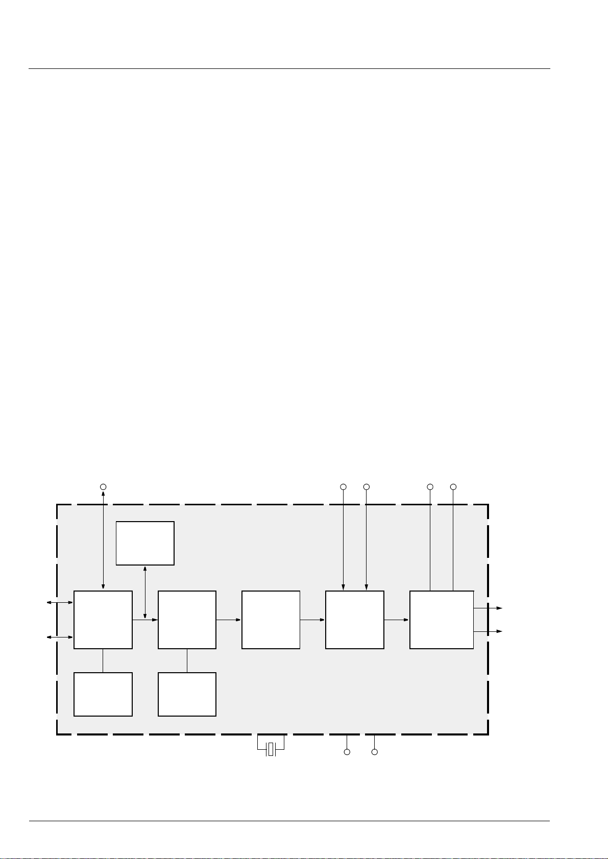
The UAC 3552A is the first member of M icronas’ USB
audio controller family of ICs targeting a wide variety of
audio applications on the USB. The UAC 3552A is a
single-chip, high-precisio n digital-to-ana log audio converter. It includes a high-quality audio sample rate converter and is able to su pport a wide range of sam ple
rates, as well as different audio formats.
The IC contains a complete USB transceiver that
allows direct connection to the USB. An on-chip
EEPROM allows storing of manufacturer- specific data
or product identification. The EEPROM can be programmed directly via the USB.
Baseband audio proces sing is handled by an inter nal,
powerful DSP. Apart from basic audio features, like
tone and volume control, there is enough processing
power left to realize customer-specific applications.
The audio DAC uses Micronas’ proprietary multibit
sigma-delta techniq ue. It features very low sensitivity
to clock jitter, high linearity, and a superior S/N ratio.
The UAC 3552A provides an on-chip headphone/
speaker amplifier. Moreover, mixing additional analog
audio sources to the D/A-converted signal is supported.
The IC is designed for all kinds of USB audio appl ications, such as USB active speakers, USB headphones,
and USB interfaces to home stereo equipment, etc.
Any existing analog speaker set can easily be
upgraded to USB by just including the UAC 3552A
according to the application circuit on page 27. No
software development is required, bec ause all drivers
are already par t of the operating system which supports USB (e. g. Windows™ 98).
D+
D
HID IO External Loop-through Filter
EEPROM
USB
Interface
−
DSP
ROMROM
DAC
Analog Input
Input
Select
and
Mixing
+5 V GND
Volu me
and
Headphone
Amplifier
OUTL
OUTR
Fig. 1–1: Block diagram of the UAC 3552A
4 Micronas
Page 5

PRELIMINARY DATA SHEET UAC 3552A
1.1. Features
– single-chip, USB specification 1.0/1.1 compliant,
stereo audio D/A converter
– 12-Mbit/s USB transceiver
– adaptive isochronous endpoint for USB Audio
– USB-programmable vendor IDs (1024-bit EEPROM
on chip)
– four general purpose input pins and four output pins
(human interface pins)
– customizable I/O functionality by download-software
– supports 16-bit mono/stereo and 24-bit stereo audio
data
– adaptive sample rate converter for 5 to 50 kHz input
sampling rate
– audio baseband control: bass, treble, volume, and
balance, additional analog volume, mute
– bass boost
– automatic gain control (AGC)
–“PerfectSpeaker” digital speaker equalizer
– THD better than 0.01 %, SNR of 96 dB
– integrated low-power stereo headphone amplifier
– on-chip op amps for external analog filter
– analog stereo input (AUX) with source selection and
mixing
– single 5-V power supply
USB
UAC
Active Stereo Speakers
Headphones
Stereo Equipment
Fig. 1–2: System application diagram
Micronas 5
Page 6

UAC 3552A PRELIMINARY DATA SHEET
2. Functional Description
2.1. Hardware
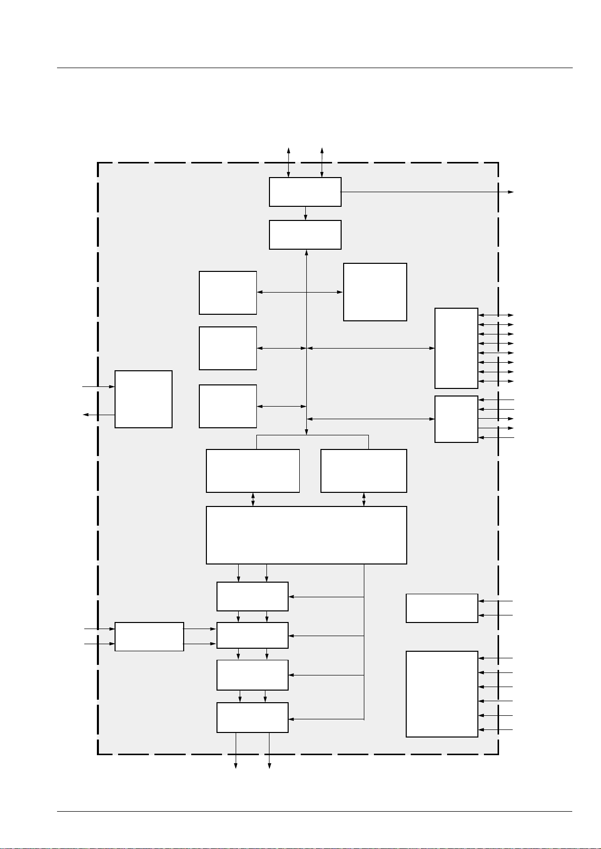
A detailed block diagram of the UAC 3552A is depicted
in Fig. 2–1. The functions of the blocks are explained
in the following sections.
2.1.1. USB Interface
2.1.1.1. Transceiver
The differential input receiver is used to accept the
USB data signal acco rding to the full- speed (12 MB/s)
USB driver characteristics (USB SPEC 1.1 - 7.1.4).
2.1.1.2. Interface Engine
The interface engine comprises two major sections:
the transceiver logic and th e receiver logic. T he transceiver logic transmits data packets built in memory by
the microcontroller. These packets are converted from
a serial to a p arallel data stream. This in cludes NRZI
encoding, bit stuffing, CRC-computation, and addition
of SYNC field and EOP. The r eceiver logic will receive
USB data and stores these packets in its memor y for
processing by the microcont roller. Serial USB data is
converted to a byte-wide parallel data stream and
stored in system memory. In addition to USB basic
data decoding, the Rx lo gic performs a PID check an d
protocol layer checks.
The ROM contains the US B drivers for the microcontroller as well as the complete de scriptor table in cluding the report descriptor for the HID-clas s. So me parts
of the descriptor which are subjected to be changed by
the customer, however, reside in the EEPROM.
The EEPROM is built to keep sta tic customer-related
data that will customize the UAC 3552A-based USB
device during production.
The 128
cific information of the USB device descriptor, like vendor ID, product ID, a s well as stri ngs for manufacturer,
product and serial number. Apart from this USBrelated information, th e EEP ROM holds cus to m er -s p ecific parameters for the PerfectSpeaker equalizer.
The UAC 3552A is shipped with a preprogrammed
EEPROM that allows normal US B functionality even if
no reprogramming is performed on the customer’s
side.
The EEPROM can be programm ed vi a US B by means
of UAC 3552A application tools.
2.1.2. Audio Control Interface
The audio control i nterface links the microcont roller to
the DSP and is u sed to ini tial ize the DS P and to tran smit audio-related USB control data, like volume setting,
tone control etc.
×8 bit EEPROM contains the customer spe-
2.1.1.3. Microcontroller
The microcontroller manages buffers for all enabled
endpoints and int eracts with the interface engi ne. The
buffers are built and decoded in memory. This way, the
microcontroller realizes the USB protocol handling, like
USB reset, enumeration, and all c hapter 9 processing ,
error handling, as well as class-speci fic endpoint handling, like audio class and HID class. The audio-c lass
processing consists of interpreting the USB audio
commands and accordi ngly controlling the DSP-a udio
function through a de dicated a udio-contr ol-interface to
the DSP. HID class processing means polling keys providing the corresponding key-codes to the host-computer’s requests. These keys are connected to the
GPIO-pins. The RAM can be accessed by the microcontroller and by the interface-engine’s DMA-controller. All endpoint communication is rea lized with intelligent buffer management built up in the RAM.
A part of the RAM is reserved for download software.
This allows adding extra functionality to the GPIO pins,
2
C-handling or any other control of external com-
like I
ponents via USB. Downloading is handl ed by an extra
driver which allows direct RAM/ROM access via USB.
2.1.3. Audio Streaming Interface
The audio streaming interface directly connects the
serial interface engine to the DS P in order to transmit
the digital audio data. The interface collect s and buffers the burst audio data for further proce ssing by the
audio processing unit.
2.1.4. Audio Processing Unit
The audio processing unit is a powerful DSP core
which allows high-quality sample conversion, baseband audio pro ce ssin g, and i nte rpolation filt ering used
for oversampling DAC, as well as customized algorithms. For more details on the so ftware see Section
2.2.2. “Audio Processing Software” on page 11.
2.1.5. Analog Back-end
The analog back-end compr ises the audio DAC, analog filters, input mixer, op amps for optimal external
postfiltering, a nalog volume and mute, and the output
amplifier.
6 Micronas
Page 7
PRELIMINARY DATA SHEET UAC 3552A
2.1.5.1. DAC
The DAC uses oversampling technique with 3rd-order
multibit noise-shaping. This technique results in
extremely low quantization noise in the audio band.
DMINUS DPLUS
24 25
26
Transceiver
VREG
Interface
Engine
XTI
XTO
8
9
Oscillator
RAM
ROM
EEPROM
Audio Streaming
Interface
Audio Processing Unit
µC
Audio Control
Interface
GP I/O
Control
I/O
14
GPIO0
15
GPIO1
16
GPIO2
17
GPIO3
19
GPIO4
20
GPIO5
21
GPIO6
22
GPIO7
29
TEST
30
RESQ
31
SUSPEND
32
SOF
33
AUXEN
27
VDD
28
VSS
6
AVDD0
7
AVDD1
3
AVSS0
2
2
AVSS1
44
VREF
1
AGNDC
AUXL
AUXR
36
Analog Input
37
DAC
Input Mixer
Volume
Headphone
Amplifier
45
OUTL OUTR
Digital Supply
Analog
Analog
Supply
Supply
Fig. 2–1: Detailed block diagram of the UAC 3552A
Micronas 7
Page 8
UAC 3552A PRELIMINARY DATA SHEET
2.1.5.2. Analog Low-pass
The output of the DAC is filterted by an analog lowpass filter with a cut-off frequency of approximately
1.4 MHz. Thi s filter removes the high-frequency components of the noise-shaping signal.
2.1.5.3. Postfilter Op Amps
This block contains the active components for the
optional analog postfi lters. It is r ecomm ended to use a
second-order filter (see Section 4. “Applications” on
page 26) in order to attenuate the out-of-band noise
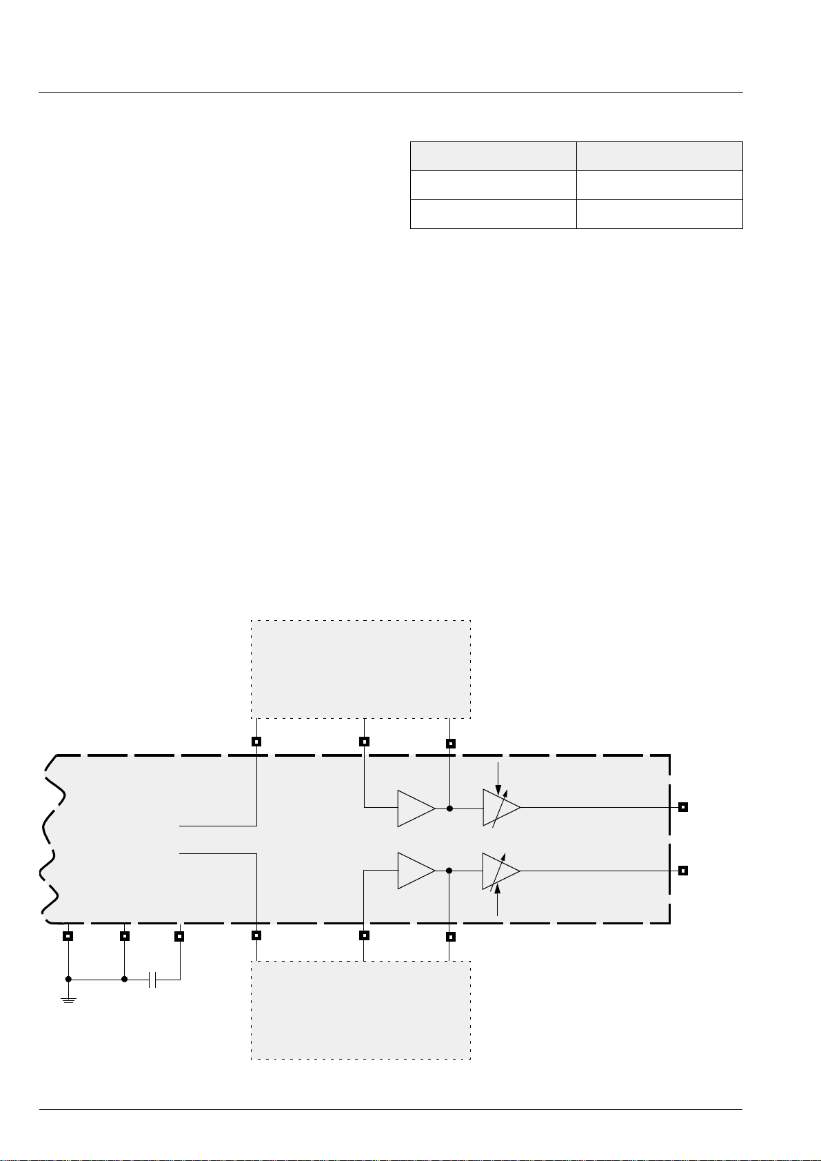
caused by the noise shaper The op amps and all I/O pins for this block are shown in Fig. 2–2.
2.1.5.4. Input Mixer
This block is used to mix the aux iliary inputs and the
signals coming from the DAC. This allows to use an
UAC 3552A-based USB speaker in a non-USB environment, like WIN 3.11 or other operating systems. On
the other hand, it allows to conn ect additional analog
sources, like CD-player or Walkman even while the
speaker is connected to th e USB. The input mixer is
hardware-controlled by the AUXEN pin.
Table 2–1: AUXEN pin
AUXEN
0 AUX not selected
1AUX selected
This allows to use a jack that switches the AUXEN to
low when an analog source i s pl ugge d i n, a ccor ding to
the application no te Section 4. “Applications” on page
26. The DAC-signal is permanently connected to the
mixer because the DAC is extremely quiet if no USB
audio is applied.
The AUXEN pin also keeps the UAC 3552A from
entering the low-power mode when an analog source
is connected. Please note that in this mode, the
UAC 3552A is not USB-compliant. If the USB is not
connected the GPIO pins work as an USB-independent volume control (see Table 2–2). BassBoost is not
supported in this mode.
UAC 3552A (Back-end)
from switch matrix
AVSS
For external components,
see section “Applications”
FOUTL
FOUTR
For external components,
see section “Applications”
FOPL FINL
−
−
FOPR
FINRAGNDCVREF
Analog Vol. L
OUTL
−
OUTR
−
Analog Vol. R
Fig. 2–2: Postfilter op amps and analog volume
8 Micronas
Page 9

PRELIMINARY DATA SHEET UAC 3552A
2.1.5.5. Ana lo g Volume Control
The analog volume control covers a range from 0 dB to
−75 dB plus an additional mute position.
The analog step size is split into a 3-dB and a 1.5-dB
range:
−75 dB...−54 dB: 3 dB step size
−54 dB...0 dB: 1.5 dB step size
The overall volume system, however, c onsi sts not onl y
of the analog volume. An additional digital volume control allows a step size of 0.5 dB over the complete
range. See Section 2.2.2.7. “V olume and Balance Control” on page 13.
Please note that analog input signals (AUXL, AUXR)
do not have the additional digital volume control.
2.1.5.6. Line-out/Headphone Amplifier
The line-out/headp hone ampl ifier outpu t is provided at
the OUTL and OUTR p ins connected either to stereo
headphones or to the power amplifier within an USB
speaker. The stereo headphones require external
Ω serial resist ors in both channel s. See Section 4.
47“Applications” on page 26.
2.1.6. General Purpose I/O
The GPIO pins are used to connect keys which are
related to the USB HID class or for vendor-specific
control functions an d LEDs in order to indicate on /off
states for example. The standard confi gurat ion def ine s
the GPIOs as four input pins (GPIO0...GPIO3) and
four output pins (GPIO4...GPIO7) . The function of the
input pins is shown in Table 2–2.
Table 2–2: Standard Key Configuration
Pin Function Key
Code
GPIO0 Volume Up
GPIO1 Volume Down 2 EA
GPIO2 MuteToggle 4 E2
GPIO3 BassBoost Toggle 8 E5
The keys are polled by the microcontroller and the corresponding key codes are transmitted to the host on
request. The relation between key code and usage ID
(see Universal Bus HID Usage Tables, Version 1.0,
Chapter 14 – Consumer Page) is defined in the HID
report descriptor (see Section 2.2.1.4. “HID Report
Descriptor” on page 11) which is transmitted to the
host along with the configuration d escriptor d uring the
bus enumeration.
1
Usage
ID
E9
When the device is not connected to USB, the functionality of the volume -control and mute pins are p reserved. In this case, however, the parameters are
directly transferred to the DSP-core. This allows using
the device in stand-alone mode providing volume and
mute control for analog sources.
The output pins ar e not predefined and therefore not
related to any USB func tio ns. They can b e set or r eset
by vendor-specific software.
The standard configuration can be changed also by
vendor-specific USB software, but in this case, Table
2–2 is no longer valid.
Micronas 9
Page 10

UAC 3552A PRELIMINARY DATA SHEET
2.1.7. Special I/O
2.1.7.1. SOF (Start of Frame)
The SOF-pin provides a 1-m s signal which is sync hronous to the USB 1-ms frame rate. It can be used for
test purpos e or as an U SB-synchronous reference for
vendor-specific external circuitry.
2.1.7.2. AUXEN
This is a digital input tha t has to be used if an analog
signal is connec ted t o the AUX R/L pi ns. It t r igg er s th e
microcontroller to switch the inp ut mixer to the analog
input (the DAC signal always remains active!) and it
keeps the device from entering the low-power mode
which can be reques ted by the host PC or by disconnecting the device from the USB.
2.1.7.3. SUSPEND
The SUSPEND pin indicates the low-power mode. It
can be used to power down external circuitry, like
power amplifiers in an USB speaker.
2.2. Software
The functionality of the UAC 3552A is main ly defined
by software. The internal
requests whereas the Audio Processing Unit processes the sound features.
2.2.1. USB Microcontroller Software
2.2.1.1. Chapter 9 Functions
The chapter 9 of the U SB Spec 1.1 defines the USB
device framework which is the middle layer of the USB
protocol hierarchy (see USB Spec 1.1 page 175). It
handles routing data between the bus interface and
various endpoints. The endpo int is a so urce or sink for
data within the device.
2.2.1.2. Device Desc rip to r
Unlike the configuration descr iptor, which is located in
ROM, the device descri ptor is mo re flexible. The manufacturer-related data are stored in the on-chip
EEPROM, and can be adapted individually. In detail
these data are
µ-controller handles the US B
Table 2–3: SUSPEND pin
SUSPEND
low normal power
high low power
2.1.8. Clock System
The UAC 3552A requires a 12-MHz clock source,
which is realized as an on-chip oscillator with external
crystal. Als o an external o scillator can be use d. In this
case, the clock has to be connected to XTI. The
12 MHz is the input clock for a PLL circuit which generates all clocks needed within the IC.
– vendor ID
– product ID
– device release number
– manufacturer string
– product string
– serial number string
A comfortable programming tool all ows this data to be
defined and writes it into the co rresponding EEPROM
location.
The UAC 3552A is shipped wi th the Micronas device
descriptor and allows USB functionality without any
EEPROM reprogramming.
2.2.1.3. String Descriptor
The string de scriptor is located i n the EEPROM. The
UAC 3552A holds three str in gs. The programm ing too l
handles the programming o f strings and wi ll take care
of string length control also.
The UAC 3552A is shipped with the Micronas string
descriptor and allows USB functionality without any
EEPROM reprogramming.
10 Micronas
Page 11
PRELIMINARY DATA SHEET UAC 3552A
2.2.1.4. HID Report Descriptor
The HID report descriptor defines the functionality of
the GPIO Pins. The basic information here are the
usage IDs for the key inputs. These IDs ar e stored in
the EEPROM and can therefore be modified if the
default configuration does not fit the application. The
UAC 3552A, however, only suppor ts the default functions: volume up/down, mute on/off and BassBoost on/
off. This means, that all nonstan dar d us age IDs will be
transmitted to the host on request and can be used
with vendor specific software, but only the default IDs
will work together with the operating system.
2.2.2. Audio Processing Software
All audio processing is realized by DSP-software,
apart f rom volume control wh ich is locate d in the analog back-end. The audio building blocks split into USBindependent features, like sample rate conversion and
oversampling filters and blocks which b elong to th e so
called USB feature unit, defined in the USB Device
Class Definition for Audio Devices. The feature unit
provides basic manipulation of the incoming logical
channels. The UAC 3552A suppor ts two logical ch annels (i.e. left & right). Multichannel or surround systems, however, can also be realized using more th an
one UAC 3552A, because ph ase or delay distor tion is
eliminated by locking the audio proc essing to the US B
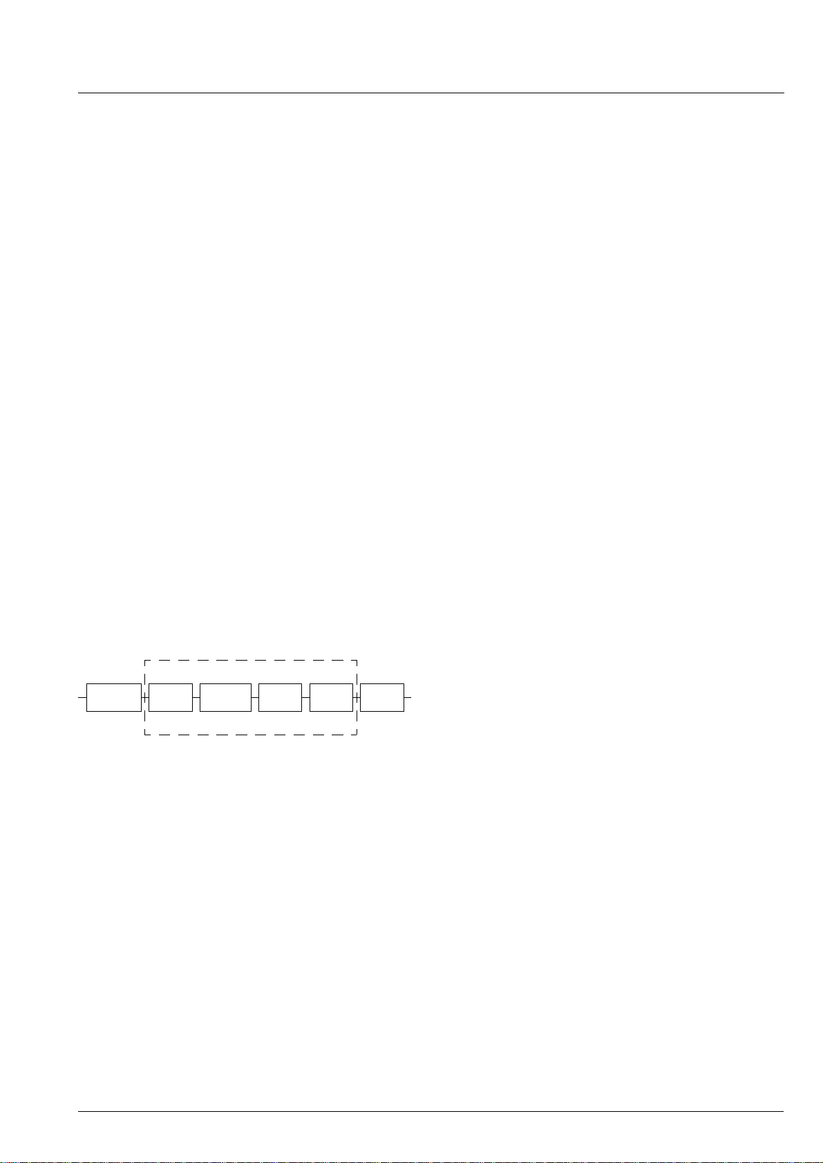
frame rate. An overview of the architecture is g iven in
Fig. 2–3.
2.2.2.1. Sample Rate Converter
The purpose of the sample rate converter is first to
transform the block transferred audio data into a continuous data stream an d second to convert all incom ing sample rates to a fixed 50-kHz sample rate. This
technique eliminates input data jitter. Furthermor e, all
audio algorithms and the DAC run on a single sample
rate and no parameter switching is required on change
of audio sampl ing rate. Further more, all audio clocks,
such as sampling clock, noise-shaping clock, and
DAC-clock can be derived from a single free-running
12-MHz oscillator. This mechanism allows continuous
input sampling rates from 5 kHz up to 50 kHz.
2.2.2.2. Automatic Gain Control
The Automatic Gain Control (AGC) is one of the building blocks of the feature unit (USB Device Class Definition for Audio Devices 1.0, page 39).
Different sound sources fairly often do not have the
same volume level. The Automatic Gain Control solves
this problem by equalizing the volume levels within a
defined range. Below a theshold level the signals are
not affected. The level-adjustment is performed with
time const an ts in orde r to a v oi d s hort-tim e ad jus tme nts
due to signal peaks.
Feature Unit
Sample Rate
Converter
AGC
Bass/Treble
Bass Boost
Fig. 2–3: Audio processing
Equalizer
Volume/
Balance
OverSampling
Micronas 11
Page 12
UAC 3552A PRELIMINARY DATA SHEET
10. 50. 100. 500. 1000. 5000. 10000.
-15
-10
-5
0
5
10
15
Hz
dB
2.2.2.3. Bass Control
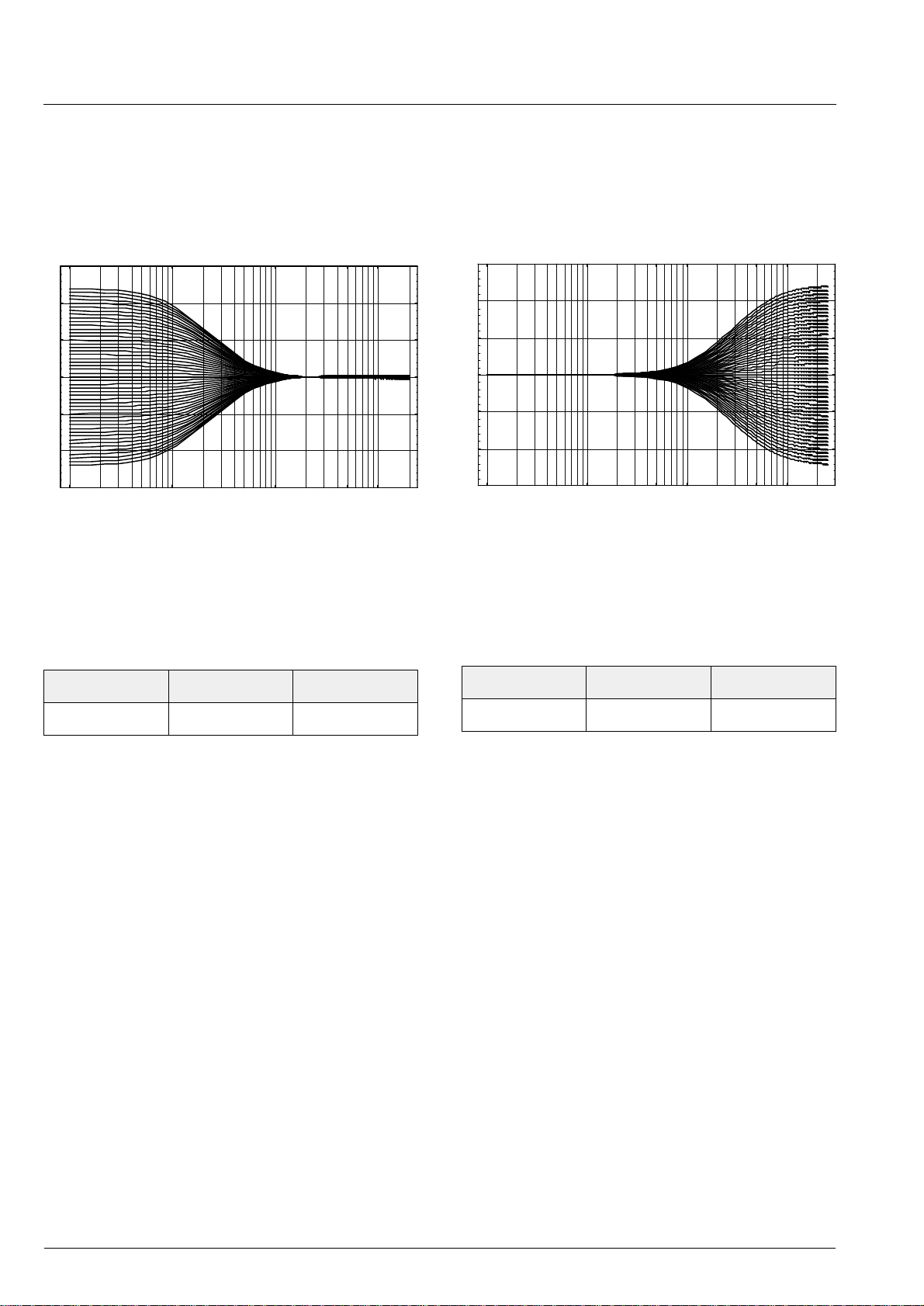
The bass control provides gain or attenuation to frequency components below a corner frequency of
120 Hz. The characteristic is shown in Fig. 2–4.
Fig. 2–4: Bass control
2.2.2.4. Treble Control
The treble control provides g ain or attenuation to frequency components above a corner frequency of
6 kHz. The characteristic is shown in Fig. 2–5.
dB
15
10
5
0
-5
-10
-15
10. 50. 100. 500. 1000. 5000. 10000.
Hz
Fig. 2–5: Treble control
The bass control works identically on both channels.
Table 2–4: Bass Control Characteristics
Min Max Step
−12 dB +12 dB 0.5 dB
The treble control works identically on both channels.
Table 2–5: Treble Control Characteristics
Min Max Step
−12 dB +12 dB 0.5 dB
12 Micronas
Page 13
PRELIMINARY DATA SHEET UAC 3552A
2.2.2.5. Bass Boost Control
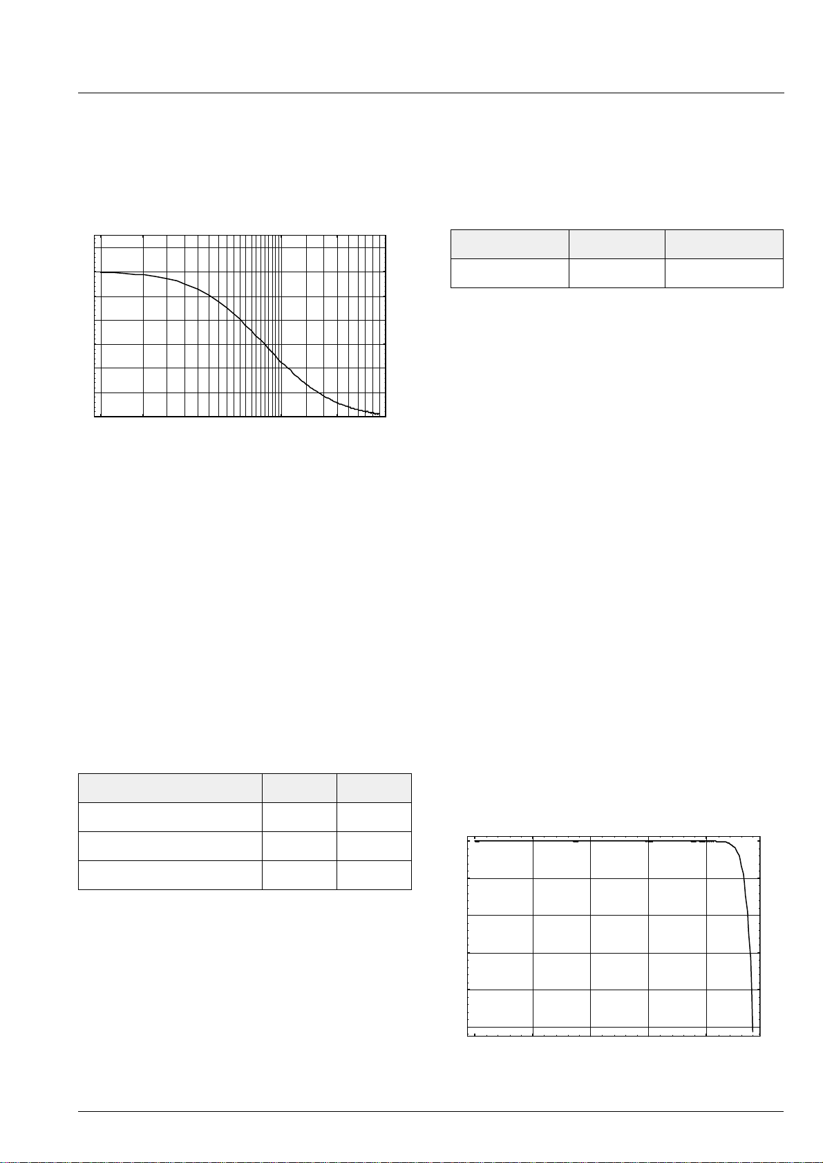
The bass boost algorithm provides an additional 12-dB
gain for the low-frequency components. The characteristic is shown in Fig. 2–6.
dB
14
12
10
8
6
4
2
0
10. 20. 50. 100. 200. 500. 1000.
Hz
Fig. 2–6: Bas s boo st
The bass boost works on both channels and can be
switched on and off under USB control.
2.2.2.7. Volume and Balance Control
The volume and balance control operate separately on
the left and right channel.
Table 2–7: Volu me and Bal anc e Cont rol
Min Max Step
−75 dB 0 dB 0.5 dB
The volume control is realized in the analo g back-end.
This preser ves high au di o qu ali ty (S NR) at l ow volume
settings because signal and noise are attenuated in
the same way, which is not the case for pure digital volume control. The UAC 3552A us es digit al volume con trol only for the fine tuning of the 0.5 dB step size. The
volume setting is smoothed by an internal ramping
algorithm in order to avoid audible clicks during volume
change.
The splitting between analog and digital volume is handled by the UAC 3552A automatically.
2.2.3. Mute Control
2.2.2.6. Parametric Equalizer
The parametric equ alizer is a non-USB audio feature.
It allows the compensation of unwanted frequency
responses of a speaker. Alternatively, frequency
responses can be set to suit individual tastes. The
equalizer consists of 5 individually adjustable bands.
The control parameters and the parameter range for
each band is shown in Table 2–6.
Table 2–6: Equalizer Parameters
Parameter Min Max
center frequency 50 Hz 15 kHz
gain/attenuation
−6dB +6dB
filter quality (Q) 0.5 3
The adjustment of the equalizer is supported by an
application program that allows to set up frequency
responses and to download the corresponding filter
coefficients into the UAC 3552A. Whe n the frequency
response fits the target, it can be programmed into the
on-chip EEPROM. The UAC 3552A is sh ipped with a
flat frequency response.
The mute control is par t of the volume system in the
UAC 3552A. It functions simultaneously on both chan nels and can be switched on and off und er USB control. As with the volume control, clicks are avoided by a
ramping algorithm.
2.2.3.1. Oversampling
The oversampling filter i ncreases the audio sampling
rate by a factor of 4. The final upsampling to the noiseshaping rate is ha ndled by a sample and hold circu it.
The pass-band ch aracter is tic of th e oversampling fi lter
is shown in Fig. 2–7.
dB
0
-0.1
-0.2
-0.3
-0.4
-0.5
0 5000 10000 15000 20000
kHz
Fig. 2–7: 1 to 4 Oversampling filter, pass-band
Micronas 13
Page 14
UAC 3552A PRELIMINARY DATA SHEET
3. Specifications
3.1. Outline Dimensions
0.06±
0.17
2333
22
0.075±
12
11
2.15
0.375
0.1±
2.0
0.1
0.2±
0.2±
13.2
34
1.75
44
1.75
1.3
1
0.2±
13.2
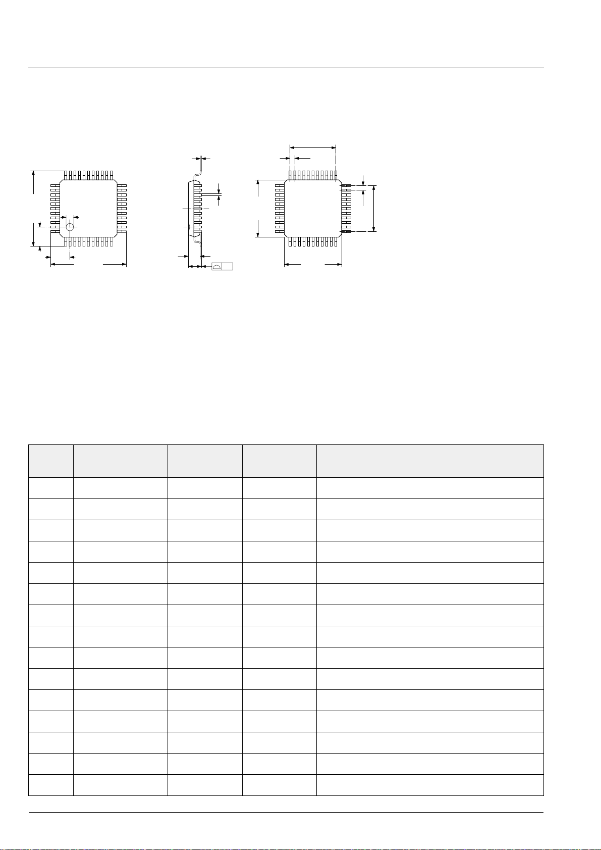
Fig. 3–1:
44-Pin Plastic Metric Quad Flat Pack
(PMQFP44)
Weight approximately 0.4 g
Dimensions in mm
3.2. Pin Connections and Short Descriptions
NC = not connected, leave vacant
LV = if not used, leave vacant
VSS = if not used, connect to VSS
0.8
10
0.1±
0.1±
0.8
10 x 0.8 = 8
0.1±
SPGS0006-3(P44)/1E
10 x 0.8 = 8
0.1±
10
X = obligatory; connect as described in
circuit diagram
VDD= conne ct to VD D
Pin
No.
Pin Name Type Connection
(If not used)
Short Description
1 AGNDC IN/OUT X Analog reference voltage
2 AVSS1 IN X VSS 1 for audio back-end
3 AVSS0 IN X VSS 0 for audio output amplifiers
4 OUTL OUT LV Audio Output: Headphone left or Speaker +
5 OUTR OUT LV Audio Output: Headphone right or Speaker
6 AVDD0 IN X VDD 0 for audio output amplifiers
7 AVDD1 IN X VDD 1 for audio back-end
8 XTI IN X quartz oscillator pin 1
9 XTO OUT X quartz oscillator pin 2
10 NC LV Not connected
11 NC LV Not connected
12 NC LV Not connected
13 NC LV Not connected
−
14 GPIO 0 IN VSS HID IO 0
15 GPIO 1 IN VSS HID IO 1
14 Micronas
Page 15

PRELIMINARY DATA SHEET UAC 3552A
Pin
No.
Pin Name Type Connection
(If not used)
Short Description
16 GPIO 2 IN VSS HID IO 2
17 GPIO 3 IN VSS HID IO 3
18 NC LV Not connected
19 GPIO 4 OUT LV HID IO 4
20 GPIO 5 OUT LV HID IO 5
21 GPIO 6 OUT LV HID IO 6
22 GPIO 7 OUT LV HID IO 7
23 TRDY OUT LV Test Output Pin
24 DMINUS IN/OUT X USB DATA MINUS
25 DPLUS IN/OUT X USB DATA PLUS
26 VREG OUT X Capacitor for internal supply
27 VDD IN X digital VDD
28 VSS IN X digital VSS
29 TEST IN X Test Enable
30 RESQ IN VDD Power On Reset, active low
31 SUSPEND OUT LV Low-Po wer Mode Indicator
32 SOF OUT LV 1-ms Start-Of-Frame Signal
33 AUXEN IN VSS Enable AUX Input
34 NC LV Not connected
35 NC LV Not connected
36 AUXL IN VSS AUX Input Left
37 AUXR IN VSS AUX Input Right
38 FOUTL OUT X Output to left external filter
39 FOPL IN/OUT X Filter op amp inverting input, left
40 FINL IN/OUT X Input for FiltoutL or
filter op amp outp ut (line out)
41 FOUTR OUT X Output to right filter op amp
42 FOPR IN/OUT X Right Filter op amp inverting input
43 FINR IN/OUT X Input for FILTOUTR or
Filter op amp output (line out)
44 VREF IN X Analog reference Ground
Micronas 15
Page 16

UAC 3552A PRELIMINARY DATA SHEET
3.3. Pin Descriptions
3.3.1. Power S upply Pins
The UAC 3552A combines various analog and digital
functions which may be used in different modes. For
optimized performance, major parts have their own
power supply pins. All VSS power supply pins must be
connected.
VDD (27)
VSS (28)
The VDD and VSS power s upply pair are connected
internally with all digital parts of the UAC 3552A.
AVDD0 (6)
AVSS0 (3)
AVDD0 and AVSS0 are separate power supply pins
that are exclusively used for the on-chip headphone/
loudspeaker amplifiers.
AVDD1 (7)
AVSS1 (2)
The AVDD1 and AVSS1 pins supply the analog audio
processing parts, except the headphone/loudspeaker
amplifiers.
3.3.2. Analog Audio Pins
AUXL (36)
AUXR (37)
The AUX pins provide two anal og stereo inpu ts. Auxiliary input signals, e.g. the output of a conventional
receiver circuit or the output of a tap e recorder c an be
connected with these inp uts. The input s ignal s have to
be connected by capacitive coupling.
FOUTL (38)
FOPL (39)
FINL (40)
FOUTR (41)
FOPR (42)
FINR (43)
Filter op amps are provided in the analog baseband
signal paths. These inverting op amps are freely
accessible for external use by these pins.
The FOUTL/R pins are connected with the buffered
output of the inter nal switch matrix. The FOPL/R-pins
are directly conne cted with the inputs of the inverting
filter op amps. The FINL/R pins are connected with the
outputs of the op amps.
OUTL (4)
OUTR (5)
The OUTL/R pins are connec ted to th e inter nal output
amplifiers. They can be used for either line-ou t or stereo headphones.
AGNDC (1)
Reference for analog audio signals. This pin is used as
reference for the internal op amps. This pin must be
blocked against VREF with a 3.3-
Note: The pin has a typical DC-level of 2.25 V. It can
be used as reference input for external op amps when
no current load is applied.
VREF (44)
Reference ground for the internal band -gap and biasing circuits. This pi n should be connected to a clea n
ground potential. Any external distortions on this pin
will affect the analog performance of the UAC 3552A.
DMINUS (24)
DPLUS (25)
Differential USB port pins.
µF capacitor.
Caution: A short circuit at these pins for more than a
momentary period may result in destruction of the
internal circuits.
XTI (8)
XTO (9)
The XTI pin is connected to the input of the internal
crystal osc illator; the XTO pin to its output. Both pins
should be directly connected to the crystal and two
ground-connected capacitors (see application diagram).
16 Micronas
Page 17

PRELIMINARY DATA SHEET UAC 3552A
3.3.3. Other Pins TEST (29)
Test enable. T his pin i s f or test purposes only and mu st
always be connected to VSS.
VREG (26)
This pin is used to connect an external buffer capacitor
to stabilize the internal supply for the USB transceiver.
RESQ (30)
This pin may be used to reset the chip.
GPIO 0 ... GPIO 7 (14,15,16,17,19,20,21,22)
These pins a re co n f ig urable t o be ei t he r input or o u tpu t
and can be used to connect audio function keys or signalling LEDs.
SUSPEND (31)
This pin indicates that the host PC sets the USB bus to
the suspend-mode state.
SOF(32)
Start of Frame Signal. 1-ms signal that can be used for
external application circuits.
AUXEN (33)
Aux enable. This pin must be conn ected to VSS if an
analog source is connec ted to the AUX input. Otherwise connect to VDD.
TRDY (23)
Test Outpu t Pin. This pin is intended for test pur poses
only and must not be connected.
3.4. Pin Configuration
VSS
AUXEN
NC
NC
AUXL
AUXR
FOUTL
FOPL
FINL
FOUTR
FOPR
FINR
VREF
AGNDC
TEST
RESQ
SUSPEND
SOF
33 32 31 30 29 28 27 26 25 24 23
34
35
36
37
38
39
40
41
42
43
44
1234567891011
AVSS1
AVSS0
UAC 3552A
OUTL
OUTR
AVDD0
VDD
AVDD1
Fig. 3–2: 44-pin PMQFP package
VREG
XTI
DPLUS
DMINUS
NC
XTO
TRDY
22
21
20
19
18
17
16
15
14
13
12
NC
GPIO 7
GPIO 6
GPIO 5
GPIO 4
NC
GPIO 3
GPIO 2
GPIO 1
GPIO 0
NC
NC
Micronas 17
Page 18
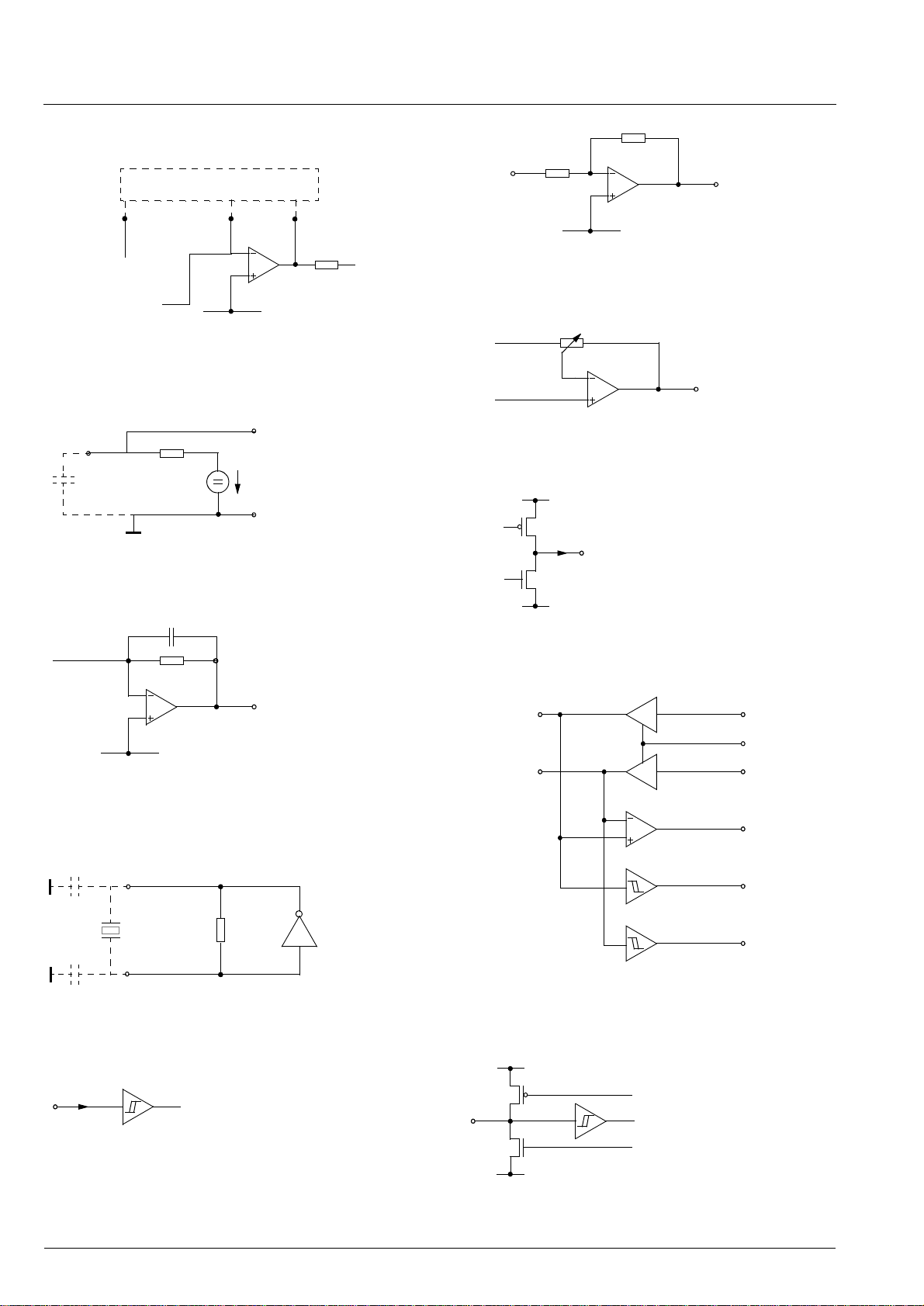
UAC 3552A PRELIMINARY DATA SHEET
Fig. 3–3: Pins FINR, FOPR, FINL, FOPL
AGNDC
FOPn
FINn
FOUTn
ext. filter network
Fig. 3–4: Pins AGNDC, VREF
125 kΩ
AVSS0/1
AGNDC
VREF
Fig. 3–5: Output Pins FOUTL, FOUTR
AGNDC
FOUTn
Fig. 3–6: Output/Input Pins XTI, XTO
500 kΩ
XTI
XTO
Fig. 3–7: Input Pins RESQ, TEST, AUXEN
3.5. Pin Circuits
AUXL/R
AGNDC
Fig. 3–8: Input Pins AUXL/R
AGNDC
OUTn
Fig. 3–9: Output Pins OUTL, OUTR
DV
SUP
P
N
GND
Fig. 3–10: Digital Output Pins SOF, SUSPEND
DPLUS
DMINUS
Fig. 3–11: Digital Input/Output Pins DMINUS,
DPLUS
DV
SUP
P
N
GND
Fig. 3–12: Input/Output Pins GPIO0...GPIO7
18 Micronas
Page 19

PRELIMINARY DATA SHEET UAC 3552A
3.6. Electrical Characteristics
3.6.1. Absolute Maximum Ratings
Symbol Parameter Pin
Name
T
A
T
S
P
Pmax
V
SUPA
V
SUPD
V
Idig
I
Idig
I
Idig
I
Odig
V
Iana
I
Iana
I
Oaudio
1)
Both have to be connected together!
2)
These pins are NOT short-circuit proof!
Ambient Operating Temperature 0 70 °C
Storage Temperatu re −40 125 °C
Powe r Dissi pat ion − 900 mW
Analog Supply Voltage
1)
AVDD0/1 −0.3 6 V
Digital Supply Voltage −0.3 6 V
Input Voltage, all digital inputs −0.3 V
Input Current, all digital inputs −5+0.5mA
Input Current, all digital outputs −88 mA
Output Current, all digital outputs −14.8 14.8 mA
Input Voltage, all analog inputs −0.3 V
Input Current, all analog inputs −5 −5mA
Output Current, audio output
2)
OUTL/R 0.2 A
Min. Max. Unit
+ 0.3 V
SUPD
+ 0.3 V
SUPA
Stresses beyond those listed in the “Absolute Maximum Ratings” may cause per m ane nt dam age to the device. This
is a stress rating onl y. Functional operation of the device at these or any ot her c onditions beyond those indi cated in
the “Rec ommended O perating Conditio ns/Characteris tics” of this s pecification is not implied. Exposure to absolute
maximum ratings conditions for extended periods may affect device reliability.
Micronas 19
Page 20
UAC 3552A PRELIMINARY DATA SHEET
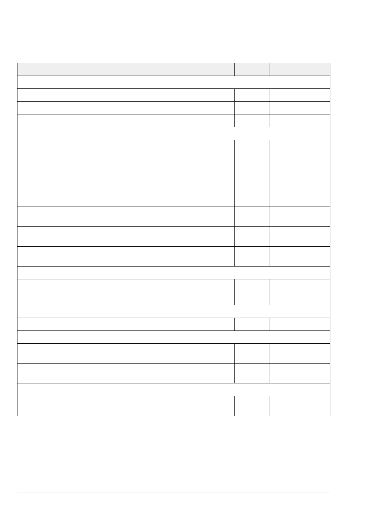
3.6.2. Recommended Operating Conditions
Symbol Parameter Pin Name Min. Typ. Max. Unit
Temperature Ranges and Supply Voltages
T
A
V
SUPA1
V
SUPD
Ambient Temperature Range 0 70 °C
Analog Audio Supply Voltage AVDD0/1 4.5 5.0 5.5 V
Digital Supply Voltage VDD 4.5 5.0 5.5 V
Relative Supply Voltages
V
SUPA
Analog Audio Supply Voltage in
relation to the Digital Supply Voltage
V
IL
V
IH
V
RIL
Input Voltage Low GPI[7:0],
Input Voltage high GPI[7:0],
Reset Input high-low transition
voltage
V
RIH
Reset Input low-high transition
voltage
T
RL
Reset low time after VDD stable
and oscillator start-up
AVDD0/1 V
SUPD
5.5 V
−0.25 V
0.25 V
AUXEN,
0.75 V
AUXEN
RESQ 0.45 V
RESQ 0.8 V
RESQ 5 µs
SUPD
SUPD
SUPD
SUPD
Analog Reference
C
AGNDC1
C
AGNDC2
Analog Reference Capacitor AGNDC 1.0 3.3 µF
Analog Reference Capacitor AGNDC 10 nF
Analog Audio Inputs
V
AI
Analog Input Voltage AC AUXL/R 0.525 1.05 V
Analog Filter Input and Output
Z
Z
AFLO
AFLI
Analog Filter Load Output
Analog Filter Load Input
Analog Audio Output
Z
AOL_HP
Analog Output Load HP
Ω Series Resistor required)
(47
rms
1)
1)
FOUTL/R 7.5
FINL/R 5.0
OUTL/R 32
400
6
7.5
kΩ
pF
kΩ
pF
Ω
pF
20 Micronas
Page 21

PRELIMINARY DATA SHEET UAC 3552A
Symbol Parameter Pin Name Min. Typ. Max. Unit
Quartz Characteri st ics
T
AC
F
P
Ambient Temperature Range 0 70 °C
Load Resonance Frequency
at C
∆F/F
∆F/F
s
s
Accuracy of Adjustment −20 20 ppm
Frequency Variation
versus Temperature
R
EQ
C
0
Equivalent Series Resistance 12 30 Ω
Shunt (parallel) Capacitance 3 5 pF
Voltage Regulator
C
VREG1
C
VREG2
Voltage Regulator Capacitor V REG 1 .0 3.3 µF
Voltage Regulator Capacitor V REG 10 nF
Transceiver
R
C
USB
USB
Input Serial Resistance DPLUS/
Shunt Capacitor DPLUS/
= 20 pF
l
DMINUS
DMINUS
12 MHz
−20 20 ppm
24
±0.5 %)
(
Ω
22 pF
1)
Please refer to Section 4.1. “Recommended Low-Pass Filters for Analog Outputs” on page 26.
Micronas 21
Page 22
UAC 3552A PRELIMINARY DATA SHEET
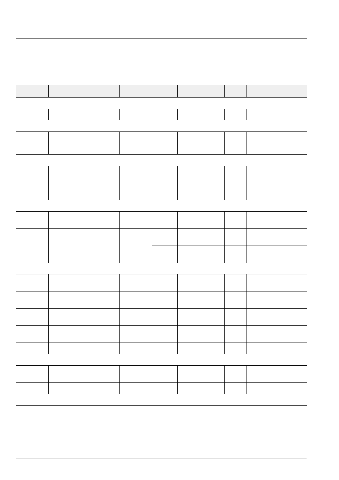
3.6.3. Characteristics
= 0 to 70 °C, V
At T
A
V
SUPD=VSUPA
= 5.0 V, quartz frequency = 12 MHz, duty cycle = 50 %, positive current flows into the IC
= 4.75 V to 5.25 V, V
SUPD
= 4.75 V to 5.25 V; typical values at TJ=27°C,
SUPA
bass/treble: 0 dB, bass boost: off, AGC: off, equalizer: off
Symbol Parameter Pin Name Min. Typ. Max. Unit Test Conditions
Digital Supply
I
VDD
Current Consumption
Digital Input Pin
I
I
Input Leakage Current GPIO[7:0],
Digital Output Pin
V
OH
V
OL
Output High Voltage GPIO[7:0],
Output Low Voltage 0.4 V
Analog Supply
I
AVDD
Current Consumption
Analog Audio
– Leakage
1)
VDD 100 125.5 mA V
±1 µAV
AUXEN,
SUPD
GND
=5 V
≤ VI ≤ V
RESQ
SUSPEND,
V
SUPD
− 0.4
VI
out
=8mA
SOF
11
2
15 mA
mA
SUSPD = 0, Mute
SUSPD = 1, Mute
SUP
PSRR
AA
Power Supply Rejection
Ratio for Analog Audio
Output
Reference Frequency Generation
V
DCXTI
C
LI
C
LO
V
XTALOUT
DC Voltage at Oscillator
Pins
Input Capacitance at
Oscillator Pin
Input Capacitance at
Oscillator Pin
Voltage Swing at Oscillator
Pins (peak-peak)
Oscillator Start-Up Time 10 ms
EEPROM
EEPROM unpowered data
retention
Number of write cycles 100
1)
no load attached to GPIO’s
AVDD0/1,
50 dB 1 kHz sine at
OUTL/R
20 dB ≤ 100 kHz sine at
XTI/O 0.5 *
V
SUPA
V
XTI 3 pF
XTO 3 pF
XTI/O 0.6 *
V
SUPA
1.0 *
V
SUPA
V
10 year
100 mV
100 mV
rms
rms
22 Micronas
Page 23

PRELIMINARY DATA SHEET UAC 3552A
Symbol Parameter Pin Name Min. Typ. Max. Unit Test Conditions
USB Transceiver
V
R
REG
O
Regulator Voltage VREG 3.25 3.4 3.55 V CL=1µF
Driver Output Resi sta nc e
including the 24-Ω external
DPLUS/
DMINUS
serial resistor
/ t
t
r
f
Rise and Fall Times DPLUS/
DMINUS
MA_TRTF Rise/Fall Time Matching DPLUS/
DMINUS
V
XOVER
V
CM_DREC
V
T_SREC
Crossover Voltage DPLUS/
DMINUS
Differential Receiver
Common-Mode Rang e
Single-ended Receiver
Threshold Voltage
DPLUS/
DMINUS
DPLUS/
DMINUS
Analog Audio
V
AGNDC
R
IAUX
Analog Refe renc e Voltage AGNDC 2.2 5 V RL >> 10 MΩ,
Input Resistance at
AUXL/R 12.1
Input Pins
28 43 Ω static, LOW or HIGH
420nsC
90 111.1 % C
=50 pF,
L
driver mode
=50 pF,
L
driver mode
1.3 2.0 V CL=50 pF,
driver mode
0.8 2.5 V
0.8 2.0 V
referred to VREF
11.6
15 17.9
19.0
kΩ
kΩ
TJ = 27 °C
TA = 0 to 70 °C
Input selected,
SUSPD = 0
± 10 µA,
i =
referred to VREF
R
OOUT
R
OFILT
V
OffI
V
OffO
V
OffFI
V
OffFO
dV
DCPD
24.2
23.3
30 35.8
37.9
kΩ
kΩ
= 27 °C
T
J
TA = 0 to 70 °C
Input not selected
SUSPD = 1
± 10 µA,
i =
referred to VREF
Output Resistance at
Output Pins
OUTL/R 700 Ω TJ = 27 °C
SUSPD = 1
± 200 µA,
i =
referred to VREF
Output Resistance of
Filter Pins
FINL 15 kΩ SUSPD = 1, Mute
± 10 µA,
i =
referred to VREFFINR 11.25 kΩ
Offset Voltage at Input Pins AUXL/R −20 20 mV SUSPD = 0,
referred to AGNDC
Offset Voltage at
Output Pins
Offset Voltage at
Filter Output Pins
Offset Voltage at
Filter Input Pins
Difference of DC Voltage at
Output Pins after Back-end
Low Power Sequence
OUTL/R −10 10 mV SUSPD = 0, Mute
referred to AGNDC
FOUTL/R −20 20 mV SUSPD = 0,
referred to AGNDC
FINL/R −20 20 mV SUSPD = 0,
referred to AGNDC
OUTL/R −10 10 mV Analog Gain = Mute,
SUSPD switched from
0 to 1
Micronas 23
Page 24

UAC 3552A PRELIMINARY DATA SHEET
Symbol Parameter Pin Name Min. Typ. Max. Unit Test Conditions
R
D/A
A
D/A
BW
THD
SNR
SNR
AUX
HP
AUX
1
D/A Pass Band Ripple OUTL/R,
FOUTL/R
0.01 dB 0...22 kHz
(no external filters
used)
D/A Stop Band Attenuation 60 dB 31 kHz...164 kHz
(no external filters
used)
Bandwidth for
Auxiliary I nputs
AUXL/R,
FINL/R
760 kHz
Total Harmonic Distortion OUTL/R 0.05 % BW = 20 Hz...0.5 fs,
unweighted, R
(47 Ω series resistor
≥ 32 Ω
L
required),
Analog Gain = 0 dB,
−3dBFS
Signal-to-Noise Ratio from
Analog Input to Outputs
AUXn,
OUTL/R
Input 1 kHz at
96 dB input −40 dB below
1.05 V
rms
Signal-to-Noise Ratio OUTL/R 89 91 dB RL≥ 32 Ω
(external 47 Ω series
resistor required)
BW =20Hz...0.5fs
unweighted,
Analog Gain = 0 dB,
Input =
−20 dBFS
SNR
Lev
V
AO
G
AUX
P
HP
2
Mute
Signal-to-Noise Ratio OUTL/R 58 62 dB RL≥ 32 Ω (external
47 Ω series resistor
required)
BW = 20 Hz..0.5 fs
unweighted
Analog Gain=
Input =
−40.5dB,
−3dBFS
Mute Level OUTL/R −110 dBV BW = 20 Hz...22 kHz
unweighted, no digital
input signal,
Analog Gain = Mute
Analog Output Voltage AC OUTL/R 1.0 1.05 1.1 V
rms
RL > 5 kΩ,
Analog Gain = 0 dB
Input = 0 dBFS digital
Gain from A uxi liary Input s to
Outputs
AUXL/R,
OUTL/R
−0.5 0 0.5 dB f = 1 kHz, sine wave,
>5kΩ
R
L
0.5 V
to AUXL/R
rms
Output Power (Headphone) OUTL/R 12 mW RL = 32 Ω,
Analog Gain = +2 dB,
distortion < 1%,
external 47 Ω series
resistor required
24 Micronas
Page 25

PRELIMINARY DATA SHEET UAC 3552A
Symbol Parameter Pin Name Min. Typ. Max. Unit Test Conditions
G
AO
dG
AO1
dG
AO2
E
GA1
E
GA2
E
GA3
E
dGA
XTALK
XTALK
Analog Output Gain
OUTL/R −75 18 dB
Setting Range
Analog Output Gain
Step Size
Analog Output Gain
Step Size
OUTL/R 3.0 dB Analog Gain:
−75 dB...-54 dB
OUTL/R 1.5 dB Analog Gain:
−54 dB...+18 dB
Analog Output Gain Error OUTL/R −2 2 dB Analog Gain = −54dB
Analog Output Gain Error OUTL/R −1 1 dB Analog Gain = −45dB
Analog Output Gain Error OUTL/R −0.5 0.5 dB Analog Gain = −39 dB
Analog Output Gain
OUTL/R −0.5 0.5 dB Analog Gain = −48 dB
Step Size Error
Crosstalk
HP
Left/Right Channel
(Headphone)
OUTL/R −70 −80 dB f = 1 kHz, sine wave,
OUTL/R: R
(47 Ω series resistor
required)
Analog Gain = 0 dB,
Input =
0.7 V
rms
Crosstalk betwee n
2
Input Signal Pairs
AUXnL/R −70 −80 dB f = 1 kHz, sine wave,
FOUTL/R: R
OUTL/R: R
(47-Ω series resist or
required)
Analog Gain = 0 dB,
Input =
0.7 V
rms
≥ 32 Ω
L
−3 dBFS or
to AUXL/R
> 7.5 kΩ
L
≥ 32 Ω
L
−3 dBFS and
to AUXL/R
Micronas 25
Page 26
UAC 3552A PRELIMINARY DATA SHEET
330 pF
15 kΩ
15 kΩ
1st-order
−
FINL(R)FOPL(R)
FOUTL(R)
11 kΩ
220 pF11 kΩ
11 kΩ
1.0 nF
−
FINL(R)FOPL(R)
FOUTL(R)
2nd-order
AVSS
4. Applications
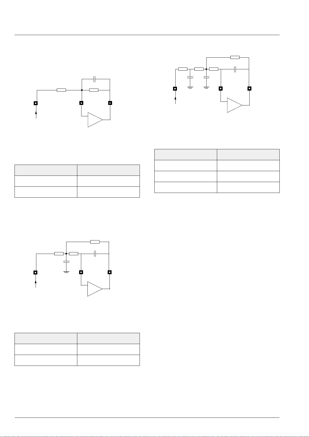
4.1. Recommended Low-Pass Filters for Analog Outputs
1)
3rd-order
7.5 kΩ
7.5 k
AVSS
Ω 7.5 kΩ
1.8 nF1.8nF
15 kΩ
120 pF
Fig. 4–1: 1st-order low-pass filter
Table 4–1: Attenuation of 1st-order low-pass filter
Frequency Gain
24 kHz
30 kHz
−2.2 dB
−3.0 dB
FOUTL(R)
FINL(R)FOPL(R)
−
Fig. 4–3: 3rd-order low-pass filter
Table 4–3: Attenuation of 3rd-order low-pass filter
Frequency Gain
18 kHz 0.17 dB
24 kHz
30 kHz
−0.23 dB
−3.00 dB
Fig. 4–2: 2nd-order low-pass filter
Table 4–2: Attenuation of 2nd-order low-pass filter
Frequency Gain
24 kHz
30 kHz
1)
without deemphasis circuit
26 Micronas
−1.5 dB
−3.0 dB
Page 27
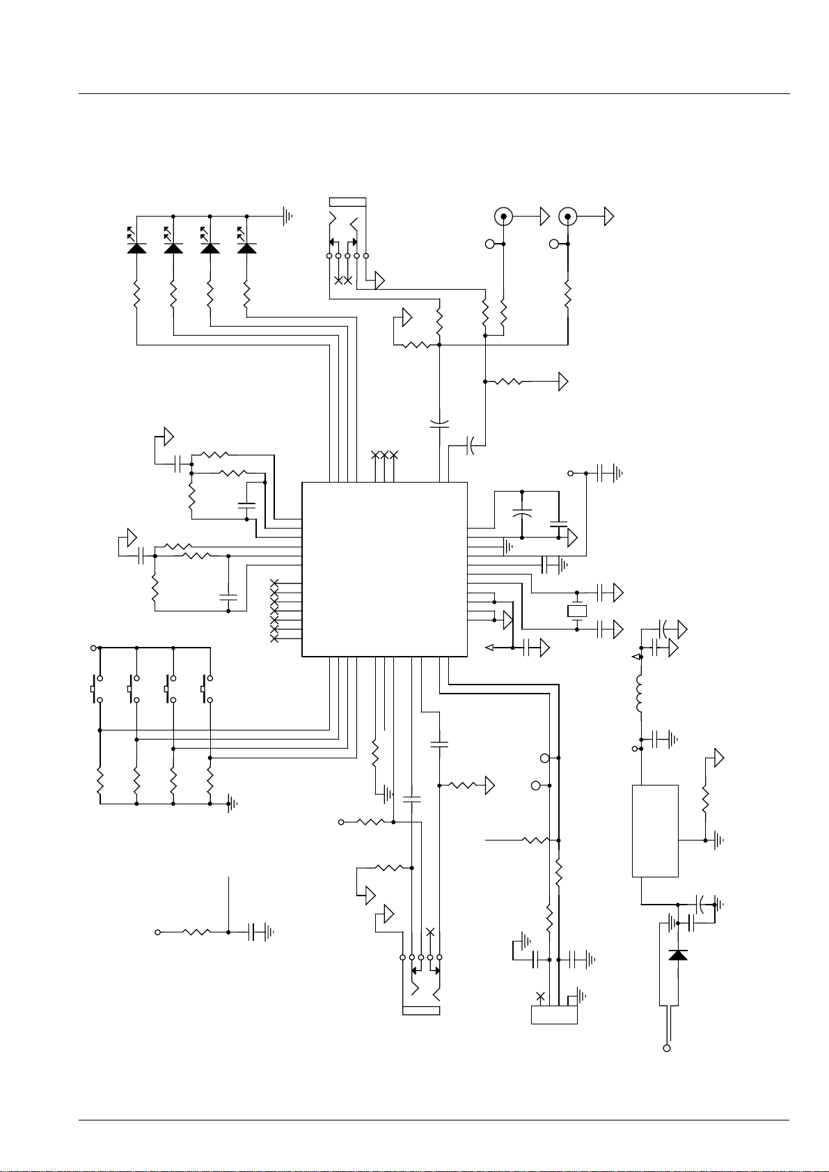
PRELIMINARY DATA SHEET UAC 3552A
q
q
g
g
5Vana
g
g
g
g
R21
11k
LM7805
g
4.2. T ypical Application
5Vdi
S1
11k
R1
1k
R4
C1
S2
Volume up
11k
R3
D1 LED
1n
11k
R5
Volume down
5Vdi
D2 LED
R81kR13
1n
C3
11k
R10
R7
11k
R9
11k
S3
Mute
11k
R6
R2
1k
R12
11k
R14
C4
S4
Bass Boost
11k
R11
220k
D3 LED
11k
220p
res
C5
1k
R15
220p
C2
D4 LED
470n
38
39
40
41
42
43
10
11
12
13
18
34
35
U1
J7
23451
GPIO6GPIO1
GPIO7
21
22
GPIO6
GPIO7
FoutL
FopL
FinL
FoutR
FopR
FinR
NC0
NC1
NC2
NC3
NC4
NC5
NC6
GPIO014GPIO115GPIO216GPIO3
GPIO0
5Vdi
GPIO5
GPIO4
19
20
GPIO4
GPIO5
17
GPIO3
GPIO2
R16
150k
PHONEJACK STEREO SW
R19
31
23
32
SOF
TRDY
Suspend
UAC 3552A
TEST29RES#
AUXEN33AUXL36AUXR
30
res
test
1k
R17
auxen
470n
C6
R18
11k
J13
RCA left
1
J12
left
+
5
4
OUTL
OUTR
dminus24dplus
25
23451
47
R22
C9
160u/16V
160u/16V
+
UAC3552A
AGNDC
1
VREF
44
VSS
28
VDD
27
VREG
26
XTO
9
XTI
8
AVDD1
7
AVDD0
6
AVSS0
3
AVSS1
2
5Vana
47
R20
1k
C8
37
470n
C7
680
R24
R23
C10
VREG
1k
VREG
J14
R25
+
1.5k
C11
J16
D-
22p
J17
C16
D+
1
1
ht
ri
680
R28
5Vdi
C14
3.3u/16V
470n
Y1
100n
1
24 0.5%
R26
D-
D+
J18
RCA right
10n
24 0.5%
R27
22p
C16
22p 22p
C17 C18
12MHz
100n
U2
L1
Ferrite bead
5Vdi
2
1
VOUT
VIN
+C21
C20
C19
47u/16V
100n
100n
GND
3
C22
D5
le connection point
sin
R29
47u/16V
+ C23
100n
1n4001
123
J11
PHONEJACK STEREO SW
J15
4
USB series B
P1
8VDC
Fig. 4–4: Application circuit
Micronas 27
Page 28

UAC 3552A PRELIMINARY DATA SHEET
5. Data Sheet History
1. Preliminary data sheet: “UAC 3552A Universal
Serial Bus DAC, Nov. 9, 1999, 6251-487-1PD. First
release of the preliminary data sheet.
Micronas GmbH
Hans-Bunte-Strasse 19
D-79108 Freiburg (Germany)
P.O. Box 840
D-79008 Freiburg (Germany)
Tel. +49-761-517-0
Fax +49-761-517-2174
E-mail: [email protected]
Internet: www.micronas.com
Printed in Germany
Order No. 6251-487-1PD
All information and data contained in this data sheet are without any
commitment, are not to be considered as an offer for conclusion of a
contract, nor shall they be construed as to create any liability. Any new
issue of this data sheet invalidates previous issues. Product availability
and delivery are exclusively subject to our respective order confirmation
form; the same applies to orders based on development samples delivered. By this publication, Micronas GmbH does not assume responsibility for patent infr ingements or other right s of third parties whic h may
result from its use.
Further, Micronas GmbH reserves the right to revise this publication and
to make changes to its conte nt, at any t ime, withou t obligatio n to noti fy
any person or entity of such revisions or changes.
No part of this publication may be reproduced, photocopied, stored on a
retrieval system, or transmitted without the express written consent of
Micronas GmbH .
28 Micronas
 Loading...