

Page 1

INTEGRATED CIRCUITS
DATA SH EET
UAA3201T
UHF/VHF remote control receiver
Product specification
Supersedes data of 1995 May 18
File under Integrated Circuits, IC18
2000 Apr 18
Page 2

Philips Semiconductors Product specification
UHF/VHF remote control receiver UAA3201T
FEATURES
• Oscillator with external Surface Acoustic Wave
Resonator (SAWR)
• Wide frequency range from 150 to 450 MHz
• High sensitivity
• Low power consumption
APPLICATIONS
• Car alarm systems
• Remote control systems
• Security systems
• Gadgets and toys
• Telemetry.
• Automotive temperature range
• Superheterodyne architecture
• Applicable to fulfil FTZ 17 TR 2100 (Germany)
• High integration level, few external components
• Inexpensive external components
• IF filter bandwidth determined by application.
GENERAL DESCRIPTION
The UAA3201T is a fully integrated single-chip receiver,
primarily intended for use in VHF and UHF systems
employing direct AM Return-to-Zero (RZ) Amplitude Shift
Keying (ASK) modulation.
QUICK REFERENCE DATA
SYMBOL PARAMETER CONDITIONS MIN. TYP. MAX. UNIT
V
CC
I
CC
P
ref
supply voltage 3.5 − 6.0 V
supply current − 3.4 4.8 mA
input reference sensitivity f
= 433.92 MHz;
i(RF)
−−−105 dBm
data rate = 250 bits/s;
BER ≤ 3 × 10
T
amb
ambient temperature −40 − +85 °C
−2
ORDERING INFORMATION
TYPE
NUMBER
NAME DESCRIPTION VERSION
PACKAGE
UAA3201T SO16 plastic small outline package; 16 leads; body width 3.9 mm SOT109-1
2000 Apr 18 2
Page 3
Philips Semiconductors Product specification
UHF/VHF remote control receiver UAA3201T
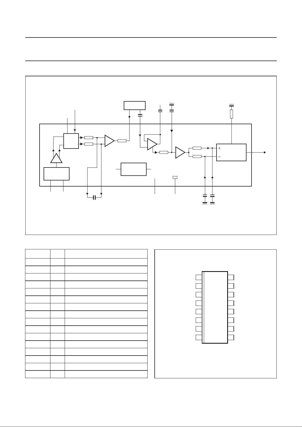
BLOCK DIAGRAM
V
C19
C12
CC
C17
R1
101112
handbook, full pagewidth
RF_IN
V
EM MIXIN
IF FILTER
FA13LIN LFB CPC CPO
161415
IF AMPLIFIER
×
MIXER
BUFFER
V
OSCILLATOR
OSC OSE MON MOP CPACPB
C7
PINNING
SYMBOL PIN DESCRIPTION
MON 1 negative mixer output
MOP 2 positive mixer output
V
CC
3 positive supply voltage
OSC 4 oscillator collector
OSE 5 oscillator emitter
V
EE
6 negative supply voltage
CPB 7 comparator input B
CPA 8 comparator input A
DATA 9 data output
CPO 10 comparator offset adjustment
CPC 11 comparator input C
LFB 12 limiter feedback
LIN 13 limiter input
MIXIN 14 mixer input
V
EM
15 negative supply voltage for mixer
FA 16 IF amplifier output
CC
LIMITER
BAND GAP
REFERENCE
V
ref
345 12
V
Fig.1 Block diagram.
CC
BUFFER
UAA3201T
V
EE
COMPARATOR
768
C13
UAA3201T
MED897
MON
MOP
V
CC
OSC
OSE
V
EE
CPB
CPA
C14
1
2
3
4
5
6
7
8
Fig.2 Pin configuration.
DATA
9
data
MHB679
16
FA
15
V
EM
14
MIXIN
13
LIN
12
LFB
11
CPC
10
CPO
9
DATA
2000 Apr 18 3
Page 4

Philips Semiconductors Product specification
UHF/VHF remote control receiver UAA3201T
FUNCTIONAL DESCRIPTION
The RF signal is fed directly into the mixer stage where it
is mixed down to nominal 500 kHz IF by the integrated
oscillator controlledby anexternalSAWR (seeFig.1). The
IF signalisthenpassedtotheIF amplifierwhichincreases
the level. A 5th-order elliptic low-pass filter acts as main
IF filtering. The output voltage of that filter is demodulated
by a limiter that rectifies the incoming IF signal. The
demodulated signal passes two RC filter stages and is
thenlimited by a data comparator which makes it available
at the data output.
Mixer
The mixer is a single balanced emitter coupled pair with
internally set bias current. The optimum impedance is
320 Ω at 430 MHz. Capacitor C5 (see Fig.9) is used to
transform a 50 Ω generator impedance to the optimum
value.
Oscillator
The oscillator consists of a transistor in common base
configuration and a tank circuit including the SAWR.
Resistor R2 (see Fig.9) is used to control the bias current
through the transistor. Resistor R3 is required to reduce
unwanted responses of the tank circuit.
IF amplifier
The IF amplifier is a differential input, single-ended output
emitter coupled pair. It is used to decouple the first and the
second IF filter and to provide some additional gain in
order to reduce the influence of the noise of the limiter on
the total noise figure.
IF filters
The first IF filter is an RC filter formed by internal resistors
and an external capacitor C7 (see Fig.1).
The second IF filter is an external elliptic filter. The source
impedance is 1.4 kΩ and the load is high-impedance. The
bandwidth of the IF filter in the application and test circuit
(see Fig.9) is 800 kHz due to the centre frequency spread
of the SAWR. It may be reduced when SAWRs with less
tolerances are used or temperature range requirements
are lower. A smaller bandwidth of the filter will yield a
higher sensitivity of the receiver. As the RF signal is mixed
down to a low IF signal there is no image rejection
possible.
Limiter
The limiting amplifier consists of three DC coupled
amplifier stages with a total gain of 60 dB. A Received
Signal Strength Indicator (RSSI) signal is generated by
rectifying the IF signal. The limiter has a lower frequency
limitof 100 kHz which can be controlled by capacitors C12
and C19. The upper frequency limit is 3 MHz.
Comparator
The2 × IF component in the RSSI signalisremoved by the
first order low-pass capacitor C17. After passing a buffer
stage the signal is split into two paths, leading via
RC filters to the inputs of a voltage comparator. The time
constant of one path (C14) is compared to the bit duration.
Consequently the potential at the negative comparator
input represents the average magnitude of the RSSI
signal. The second path with a short time constant (C13)
allows the signal at the positive comparator input to follow
the RSSI signal instantaneously. This results in a variable
comparator threshold, depending on the strength of the
incoming signal. Hence the comparator output is switched
on, when the RSSI signal exceeds its average value, i.e.
when an ASK ‘on’ signal is received.
The low-pass filter capacitor C13 rejects the unwanted
2 × IF component and reduces the noise bandwidth of the
data filter.
The resistor R1 is used to set the current of an internal
source. This current is drawn from the positive comparator
input,therebyapplyinganoffsetanddriving the output into
the ‘off’ state during the absence of an input signal. This
offset can be increased by lowering the value of R1
yieldinga higher noise immunity at the expenseofreduced
sensitivity.
Band gap reference
The band gap reference controls the biasing of the whole
circuit. In this block currents are generated that are
constant over the temperature range and currents that are
proportional to the absolute temperature.
The current consumption of the receiver rises with
increasing temperature, because the blocks with the
highest current consumption are biased by currents that
are proportional to the absolute temperature.
2000 Apr 18 4
Page 5

Philips Semiconductors Product specification
UHF/VHF remote control receiver UAA3201T
LIMITING VALUES
In accordance with the Absolute Maximum Rating System (IEC 60134).
SYMBOL PARAMETER CONDITIONS MIN. MAX. UNIT
V
CC
T
amb
T
stg
V
es
Note
1. Human body model: equivalent to discharging a 100 pF capacitor through a 1.5 kΩ series resistor.
THERMAL CHARACTERISTICS
supply voltage −0.3 +8.0 V
ambient temperature −40 +85 °C
storage temperature −55 +125 °C
electrostatic handling voltage note 1
pins OSC and OSE −2000 +1500 V
pins LFB and MIXIN −1500 +2000 V
all other pins −2000 +2000 V
SYMBOL PARAMETER CONDITIONS VALUE UNIT
R
th(j-a)
thermal resistance from junction to ambient in free air 105 K/W
DC CHARACTERISTICS
= 3.5 V; all voltages referenced to VEE; T
V
CC
= −40 to +85 °C; typical value for T
amb
=25°C; for test circuit
amb
see Fig.9; SAWR disconnected; unless otherwise specified.
SYMBOL PARAMETER CONDITIONS MIN. TYP. MAX. UNIT
V
CC
I
CC
V
OH(DATA)
supply voltage 3.5 − 6.0 V
supply current R2 = 680 Ω−3.4 4.8 mA
HIGH-level output voltage at
I
= −10 µA; note 1 VCC− 0.5 − V
DATA
CC
V
pin DATA
V
OL(DATA)
LOW-level output voltage at
I
= +200 µA; note 1 0 − 0.6 V
DATA
pin DATA
Note
1. I
is defined to be positive when the current flows into pin DATA.
DATA
2000 Apr 18 5
Page 6
Philips Semiconductors Product specification
UHF/VHF remote control receiver UAA3201T
AC CHARACTERISTICS
VCC= 3.5 V; T
conditions”; unless otherwise specified.
SYMBOL PARAMETER CONDITIONS MIN. TYP. MAX. UNIT
P
ref
P
i(max)
P
spur
IP3
mix
IP3
IF
P
1dB
t
on(RX)
Notes
1. P
is the maximum available power at the input of the test board. The Bit Error Rate (BER) is measured using the
ref
test facility shown in Fig.8.
2. Valid only for the reference PCB (see Figs 10 and 11). Spurious radiation is strongly dependent on the PCB layout.
3. The supply voltage VCC is pulsed as explained in Fig.3.
=25°C; for test circuit see Fig.9; R1 disconnected; for AC test conditions see Section “AC test
amb
input reference sensitivity BER ≤ 3 × 10⁻²; note 1 −−−105 dBm
maximum input power BER ≤ 3 × 10
−2
−−−30 dBm
spurious radiation note 2 −−−60 dBm
interception point (mixer) −20 −17 − dBm
interception point (mixer plus IFamplifier) −38 −35 − dBm
1 dB compression point (mixer) −38 −35 − dBm
receiver turn-on time note 3 −−10 ms
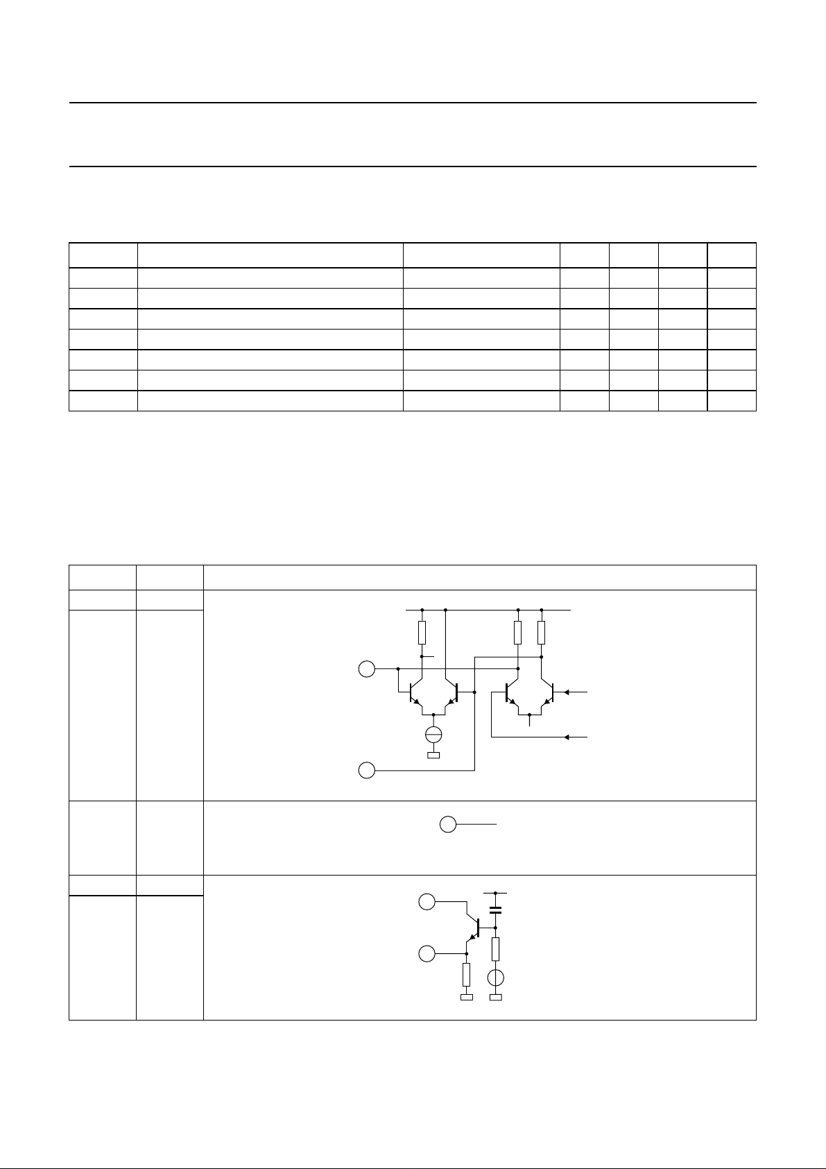
INTERNAL PIN CONFIGURATION
PIN SYMBOL EQUIVALENT CIRCUIT
1 MON
2 MOP
1
2
3V
CC
3
MHB681
4 OSC
5 OSE
4
1.5
kΩ
V
CC
V
P
1.5
kΩ
from
oscillator
buffer
MHB680
V
P
2000 Apr 18 6
5
6 kΩ
1.2 V
MHB682
Page 7

Philips Semiconductors Product specification
UHF/VHF remote control receiver UAA3201T
PIN SYMBOL EQUIVALENT CIRCUIT
6V
EE
6
MHB683
7 CPB
8CPA
9 DATA
10 CPO
V
P
150 kΩ
7
8
1 kΩ
9
150 kΩ
MHB684
V
P
MHB686
V
P
11 CPC
2000 Apr 18 7
10
MHB685
V
P
30 kΩ
11
MHB704
Page 8

Philips Semiconductors Product specification
UHF/VHF remote control receiver UAA3201T
PIN SYMBOL EQUIVALENT CIRCUIT
12 LFB
13 LIN
14 MXIN
15 V
EM
50
kΩ
12
13
14
V
P
MHB687
16 FA
15
1.4 kΩ
16
MHB688
V
P
MHB689
TEST INFORMATION
Tuning procedure for AC tests
1. Turn on the signal generator: f
= 433.92 MHz, no modulation and RF input level=1mV.
i(RF)
2. Tune capacitor C6 (RF stage input) to obtain a maximum voltage on pin LIN.
3. Check that data is appearing on pin DATA and proceed with the AC tests.
AC test conditions
The reference signal level P
for the following tests is defined as the minimum input level in dBm to give a
ref
BER ≤ 3 × 10⁻² (e.g. 7.5 bit errors per second for 250 bits/s).
2000 Apr 18 8
Page 9

Philips Semiconductors Product specification
UHF/VHF remote control receiver UAA3201T
Table 1 Test signals
TEST
SIGNAL
1 433.92 250 bits/s
FREQUENCY
(MHz)
DATA SIGNAL MODULATION
RZ signal with duty cycle of 66% for logic 1;
(square wave)
RZ signal with duty cycle of 33% for logic 0
MODULATION
INDEX
100%
2 434.02 − no modulation −
3 433.92 − no modulation −
Test results
P
is the maximum available power from signal generator 1 at the input of the test board; P2 is the maximum available
1
power from signal generator 2 at the input of the test board.
Table 2 Test results
GENERATOR
TEST
RESULT
12
Maximum input power;
see Fig.4
Receiver turn-on time;
see Fig.4 and note 1
Interception point (mixer);
see Fig.5 and note 2
Interception point (mixer plus
IF amplifier); see Fig.5 and
note 3
Spurious radiation; see Fig.6
and note 4
1 dB compression point
(mixer);
see Fig.7 and note 5
test signal 1;
= −30 dBm
P
1
(minimum P
test signal 1;
P
1=Pref
+10dB
test signal 3;
= −50 dBm
P
1
test signal 3;
P
= −50 dBm
1
max
− BER ≤ 3 × 10
(e.g. 7.5 bit errors per second for 250 bits/s)
)
− check that the first 10 bits are correct; error counting is
started 10 ms after VCC is switched on
test
signal 2;
P2=P
test
signal 2;
P2=P
IP3 = P1+1⁄2× IM3 (dB);
minimum value: IP3
1
IP3 = P1+1⁄2× IM3 (dB);
minimum value: IP3IF≥−38 dBm
1
−−no spurious radiation (25 MHz to 1 GHz) with level
higher than −60 dBm (maximum P
test signal 3;
P
= −70 dBm;
11
P12= −38 dBm
(minimum P
1dB
− (Po1+ 70 dB) − [Po2+ 38 dB (minimum P
where Po1is the output power for test signal with P
and Po2 is the output power for test signal with P
)
−2
≥−20 dBm
mix
)
spur
)] ≤ 1dB,
1dB
11
12
Notes
1. The supply voltage VCC of the test circuit alternates between ‘on’ (100 ms) and ‘off’ (100 ms); see Fig.3.
2. Differential probe of spectrum analyser connected to pins MOP and MON.
3. Probe of spectrum analyser connected to pin LIN.
4. Spectrum analyser connected to the input of the test board.
5. Probe of spectrum analyser connected to either pin MOP or pin MON.
2000 Apr 18 9
Page 10

Philips Semiconductors Product specification
UHF/VHF remote control receiver UAA3201T
(1) For test circuit see Fig.9.
(2) For BER test facility see Fig.8.
V
CC
(V)
3.5
0
3002001000
Fig.3 Timing diagram for pulsed supply voltage.
GENERATOR 1
50 Ω
TEST CIRCUIT
(1)
Fig.4 Test configuration (single generator).
MED899 - 1
t (ms)
BER TEST
FACILITY
(2)
MED900
GENERATOR 1
50 Ω
50 Ω
2-SIGNAL
POWER
COMBINER
GENERATOR 2
50 Ω
(1) For test circuit see Fig.9.
Fig.5 Test configuration (interception point).
2000 Apr 18 10
TEST CIRCUIT
(1)
∆f
∆f = 100 kHz
SPECTRUM
ANALYZER
WITH
PROBE
IM3
∆f ∆f
MED901
Page 11

Philips Semiconductors Product specification
UHF/VHF remote control receiver UAA3201T
SPECTRUM
(1) For test circuit see Fig.9.
ANALYZER
INPUT IMPEDANCE
50 Ω
TEST CIRCUIT
Fig.6 Test configuration (spurious radiation).
(1)
MED902
(1) For test circuit see Fig.9.
UNDER TEST
DEVICE
GENERATOR 1
50 Ω
TEST CIRCUIT
(1)
SPECTRUM
ANALYZER
WITH
PROBE
Fig.7 Test configuration (1 dB compression point).
SIGNAL
GENERATOR
MASTER
CLOCK
delayed
TX data
TX data
BIT PATTERN
GENERATOR
PRESET
DELAY
MED903
INTEGRATE
RX data
AND DUMP
Fig.8 BER test facility.
2000 Apr 18 11
DATA
COMPARATOR
BER TEST BOARD
to error counter
MED904
Page 12

Philips Semiconductors Product specification
UHF/VHF remote control receiver UAA3201T
APPLICATION INFORMATION
handbook, full pagewidth
FA
16
1 2 3456 78
MON MOP OSC OSE CPB CPA
3.5 V
C9
C20
L2 L3
IF
AMP
C7
RF_IN
C11C8
C10
V
15 14 13 12 11 10 9
V
CC
V
EM
MIXER
ref
C5
C19
MIXIN LIN LFB CPC CPO DATA
BAND GAP
REFERENCE
V
CC
C3C2C1
C4
L1
C6
BUFFER
OSCILLATOR
C18
L4 R2
C16
C15
LIMITER
R3
+3.5 V
C12
(1)
C17
BUFFER
UAA3201T
V
EE
C21
R1
COMPARATOR
C14 C13
data
MED896
SAWR
(1) Stray inductance.
Fig.9 Application and test circuit.
Fig.9 Application and test circuit.
2000 Apr 18 12
Page 13

Philips Semiconductors Product specification
UHF/VHF remote control receiver UAA3201T
Components and layout of printed circuit board of test circuit for f
= 433.92 MHz
i(RF)
Table 3 Components list for Fig.9
COMPONENT VALUE TOLERANCE DESCRIPTION
R1 27 kΩ±2% TC = +50 ppm/K
R2 680 Ω±2% TC = +50 ppm/K
R3 220 Ω±2% TC = +50 ppm/K
C1 4.7 µF ±20% −
≤ 1pF
≤ 1pF
−4
; f = 1 MHz
−4
; f = 1 MHz
−4
; f = 1 MHz
−4
−4
−4
; f = 1 MHz
−4
; f = 1 MHz
−4
; f = 1 MHz
−4
; f = 1 MHz
−4
; f = 1 MHz
−4
; f = 1 MHz
−4
−4
−4
; f = 1 MHz
−4
−4
; f = 1 MHz
C2 150 pF ±10% TC = 0 ±30 ppm/K; tan δ≤10 × 10
C3 1 nF ±10% TC = 0 ±30 ppm/K; tan δ≤10 × 10
C4 820 pF ±10% TC = 0 ±30 ppm/K; tan δ≤10 × 10
C5 3.3 pF ±10% TC = 0 ±150 ppm/K; tan δ≤30 × 10
C6 2.5 to 6 pF − TC = 0 ±300 ppm/K; tan δ≤20 × 10
C7 56 pF ±10% TC= 0 ±30 ppm/K; tan δ≤10 × 10
C8 150 pF ±10% TC = 0 ±30 ppm/K; tan δ≤10 × 10
C9 220 pF ±10% TC = 0 ±30 ppm/K; tan δ≤10 × 10
C10 27 pF ±10% TC = 0 ±30 ppm/K; tan δ≤20 × 10
C11 150 pF ±10% TC = 0 ±30 ppm/K; tan δ≤10 × 10
C12 100 nF ±10% tan δ≤25 × 10
C13 2.2 nF ±10% tan δ≤25 × 10
C14 33 nF ±10% tan δ≤25 × 10
−3
; f = 1 kHz
−3
; f = 1 kHz
−3
; f = 1 kHz
C15 150 pF ±10% TC = 0 ±30 ppm/K; tan δ≤10 × 10
C16 3.9 pF ±10% TC = 0 ±150 ppm/K; tan δ≤30 × 10
−3
C17 10 nF ±10% tan δ≤25 × 10
; f = 1 kHz
C18 3.3 pF ±10% TC = 0 ±150 ppm/K; tan δ≤30 × 10
C19 68 pF ±10% TC = 0 ±30 ppm/K; tan δ≤10 × 10
C20 6.8 pF ±10% TC = 0 ±150 ppm/K; tan δ≤30 × 10
C21 47 pF ±5% TC = 0 ±30 ppm/K; tan δ≤10 × 10
L1 10 nH ±10% Q
L2 330 µH ±10% Q
L3 330 µH ±10% Q
L4 33 nH ±10% Q
= 50 to 450 MHz; TC = 25 to 125 ppm/K
min
= 45 to 800 kHz; C
min
= 45 to 800 kHz; C
min
= 45 to 450 MHz; TC = 25 to 125 ppm/K
min
stray
stray
SAWR −−see Table 4
; f = 1 MHz
; f = 1 MHz
; f = 1 MHz
; f = 1 MHz
; f = 1 MHz
Table 4 SAWR data
DESCRIPTION SPECIFICATION
Type one-port (e.g. RFM R02112)
Centre frequency 433.42 MHz ±75 kHz
Maximum insertion loss 1.5 dB
Typical loaded Q 1600 (50 Ω load)
Temperature drift 0.032 ppm/K
2
Turnover temperature 43 °C
2000 Apr 18 13
Page 14

Philips Semiconductors Product specification
UHF/VHF remote control receiver UAA3201T
MBE589
RF_IN
data
n.c.
H4ACS15
UAA3201T
Fig.10 Layout top side.
MBE591
PCALH/H4ACS15
Fig.11 Layout bottom side.
2000 Apr 18 14
H4ACS15
Page 15

Philips Semiconductors Product specification
UHF/VHF remote control receiver UAA3201T
MBE590
RF_IN
C5
C4
L3
C19
L2
n.c.
C6
C15
L1
C12 C17
IC1
R1
SAWR
DATA
C13
C14
data
H4ACS15
supply
UAA3201T
Fig.12 Top side with components.
Fig.12 Top side with components.
C11
C10
C9
C21
R2
C18
C8
C2
C16
R3
L4
C20
C7
C1
MBE592
C3
PCALH/H4ACS15
Fig.13 Bottom side with components.
2000 Apr 18 15
H4ACS15
Page 16

Philips Semiconductors Product specification
UHF/VHF remote control receiver UAA3201T
PACKAGE OUTLINE
SO16: plastic small outline package; 16 leads; body width 3.9 mm
SOT109-1
Z
16
pin 1 index
1
D
c
y
9
A
2
A
1
8
e
w M
b
p
E
H
E
detail X
A
X
v M
A
Q
(A )
L
p
L
A
3
θ
0 2.5 5 mm
scale
DIMENSIONS (inch dimensions are derived from the original mm dimensions)
UNIT
mm
inches
Note
1. Plastic or metal protrusions of 0.15 mm maximum per side are not included.
A
max.
1.75
0.069
OUTLINE
VERSION
SOT109-1
A1A2A
0.25
1.45
0.10
1.25
0.010
0.057
0.004
0.049
IEC JEDEC EIAJ
076E07 MS-012
0.25
0.01
b
3
p
0.49
0.25
0.36
0.19
0.0100
0.019
0.0075
0.014
(1)E(1) (1)
cD
10.0
4.0
3.8
0.16
0.15
1.27
0.050
9.8
0.39
0.38
REFERENCES
2000 Apr 18 16
eHELLpQZywv θ
1.05
0.041
1.0
0.4
0.039
0.016
0.7
0.25
0.6
0.028
0.01 0.004
0.020
EUROPEAN
PROJECTION
0.25 0.1
0.01
0.7
0.3
0.028
0.012
ISSUE DATE
97-05-22
99-12-27
o
8
o
0
6.2
5.8
0.244
0.228
Page 17

Philips Semiconductors Product specification
UHF/VHF remote control receiver UAA3201T
SOLDERING
Introduction to soldering surface mount packages
Thistextgives a very brief insight to a complex technology.
A more in-depth account of soldering ICs can be found in
our
“Data Handbook IC26; Integrated Circuit Packages”
(document order number 9398 652 90011).
There is no soldering method that is ideal for all surface
mount IC packages. Wave soldering is not always suitable
for surface mount ICs, or for printed-circuit boards with
high population densities. In these situations reflow
soldering is often used.
Reflow soldering
Reflow soldering requires solder paste (a suspension of
fine solder particles, flux and binding agent) to be applied
totheprinted-circuitboardbyscreenprinting,stencillingor
pressure-syringe dispensing before package placement.
Several methods exist for reflowing; for example,
infrared/convection heating in a conveyor type oven.
Throughput times (preheating, soldering and cooling) vary
between 100 and 200 seconds depending on heating
method.
Typical reflow peak temperatures range from
215 to 250 °C. The top-surface temperature of the
packages should preferable be kept below 230 °C.
• Use a double-wave soldering method comprising a
turbulent wave with high upward pressure followed by a
smooth laminar wave.
• For packages with leads on two sides and a pitch (e):
– larger than or equal to 1.27 mm, the footprint
longitudinal axis is preferred to be parallel to the
transport direction of the printed-circuit board;
– smaller than 1.27 mm, the footprint longitudinal axis
must be parallel to the transport direction of the
printed-circuit board.
The footprint must incorporate solder thieves at the
downstream end.
• Forpackages with leads on four sides, thefootprintmust
be placed at a 45° angle to the transport direction of the
printed-circuit board. The footprint must incorporate
solder thieves downstream and at the side corners.
During placement and before soldering, the package must
be fixed with a droplet of adhesive. The adhesive can be
applied by screen printing, pin transfer or syringe
dispensing. The package can be soldered after the
adhesive is cured.
Typical dwell time is 4 seconds at 250 °C.
A mildly-activated flux will eliminate the need for removal
of corrosive residues in most applications.
Manual soldering
Wave soldering
Conventional single wave soldering is not recommended
forsurface mount devices (SMDs) or printed-circuit boards
with a high component density, as solder bridging and
non-wetting can present major problems.
To overcome these problems the double-wave soldering
method was specifically developed.
If wave soldering is used the following conditions must be
observed for optimal results:
Fix the component by first soldering two
diagonally-opposite end leads. Use a low voltage (24 V or
less) soldering iron applied to the flat part of the lead.
Contact time must be limited to 10 seconds at up to
300 °C.
When using a dedicated tool, all other leads can be
soldered in one operation within 2 to 5 seconds between
270 and 320 °C.
2000 Apr 18 17
Page 18

Philips Semiconductors Product specification
UHF/VHF remote control receiver UAA3201T
Suitability of surface mount IC packages for wave and reflow soldering methods
PACKAGE
WAVE REFLOW
(1)
BGA, LFBGA, SQFP, TFBGA not suitable suitable
SOLDERING METHOD
HBCC, HLQFP, HSQFP, HSOP, HTQFP, HTSSOP, SMS not suitable
(3)
PLCC
, SO, SOJ suitable suitable
LQFP, QFP, TQFP not recommended
SSOP, TSSOP, VSO not recommended
(2)
(3)(4)
(5)
suitable
suitable
suitable
Notes
1. All surface mount (SMD) packages are moisture sensitive. Depending upon the moisture content, the maximum
temperature (with respect to time) and body size of the package, there is a risk that internal or external package
cracks may occur due to vaporization of the moisture in them (the so called popcorn effect). For details, refer to the
Drypack information in the
“Data Handbook IC26; Integrated Circuit Packages; Section: Packing Methods”
.
2. These packages are not suitable for wave soldering as a solder joint between the printed-circuit board and heatsink
(at bottom version) can not be achieved, and as solder may stick to the heatsink (on top version).
3. If wave soldering is considered, then the package must be placed at a 45° angle to the solder wave direction.
The package footprint must incorporate solder thieves downstream and at the side corners.
4. Wave soldering is only suitable for LQFP, TQFP and QFP packages with a pitch (e) equal to or larger than 0.8 mm;
it is definitely not suitable for packages with a pitch (e) equal to or smaller than 0.65 mm.
5. Wave soldering is only suitable for SSOP and TSSOP packages with a pitch (e) equal to or larger than 0.65 mm; it is
definitely not suitable for packages with a pitch (e) equal to or smaller than 0.5 mm.
2000 Apr 18 18
Page 19

Philips Semiconductors Product specification
UHF/VHF remote control receiver UAA3201T
DATA SHEET STATUS
DATA SHEET STATUS
Objective specification Development This data sheet contains the design target or goal specifications for
Preliminary specification Qualification This data sheet contains preliminary data, and supplementary data will be
Product specification Production This data sheet contains final specifications. Philips Semiconductors
Note
1. Please consult the most recently issued data sheet before initiating or completing a design.
DEFINITIONS
Short-form specification The data in a short-form
specification is extracted from a full data sheet with the
same type number and title. For detailed information see
the relevant data sheet or data handbook.
Limiting values definition Limiting values given are in
accordance with the Absolute Maximum Rating System
(IEC 60134). Stress above one or more of the limiting
values may cause permanent damage to the device.
These are stress ratings only and operation of the device
attheseor at any other conditions above those given in the
Characteristics sections of the specification is not implied.
Exposure to limiting values for extended periods may
affect device reliability.
Application information Applications that are
described herein for any of these products are for
illustrative purposes only. Philips Semiconductors make
norepresentation or warranty that suchapplicationswill be
suitable for the specified use without further testing or
modification.
PRODUCT
STATUS
DEFINITIONS
product development. Specification may change in any manner without
notice.
published at a later date. Philips Semiconductors reserves the right to
make changes at any time without notice in order to improve design and
supply the best possible product.
reserves the right to make changes at any time without notice in order to
improve design and supply the best possible product.
DISCLAIMERS
Life support applications These products are not
designed for use in life support appliances, devices, or
systems where malfunction of these products can
reasonably be expected to result in personal injury. Philips
Semiconductorscustomers using or selling theseproducts
for use in such applications do so at their own risk and
agree to fully indemnify Philips Semiconductors for any
damages resulting from such application.
Right to make changes Philips Semiconductors
reserves the right to make changes, without notice, in the
products, including circuits, standard cells, and/or
software, described or contained herein in order to
improve design and/or performance. Philips
Semiconductors assumes no responsibility or liability for
theuse of any of these products, conveysnolicenceor title
under any patent, copyright, or mask work right to these
products,andmakesno representations or warranties that
these products are free from patent, copyright, or mask
work right infringement, unless otherwise specified.
(1)
2000 Apr 18 19
Page 20

Philips Semiconductors – a w orldwide compan y
Argentina: see South America
Australia: 3 Figtree Drive, HOMEBUSH, NSW 2140,
Tel. +61 2 9704 8141, Fax. +61 2 9704 8139
Austria: Computerstr. 6, A-1101 WIEN, P.O. Box 213,
Tel. +43 1 60 101 1248, Fax. +43 1 60 101 1210
Belarus: Hotel Minsk Business Center, Bld. 3, r. 1211, Volodarski Str. 6,
220050 MINSK, Tel. +375 172 20 0733, Fax. +375 172 20 0773
Belgium: see The Netherlands
Brazil: seeSouth America
Bulgaria: Philips Bulgaria Ltd., Energoproject, 15thfloor,
51 James Bourchier Blvd., 1407 SOFIA,
Tel. +359 2 68 9211, Fax. +359 2 68 9102
Canada: PHILIPS SEMICONDUCTORS/COMPONENTS,
Tel. +1 800 234 7381, Fax. +1 800 943 0087
China/Hong Kong: 501 Hong Kong Industrial Technology Centre,
72 Tat Chee Avenue, Kowloon Tong, HONG KONG,
Tel. +852 2319 7888, Fax. +852 2319 7700
Colombia: see South America
Czech Republic: see Austria
Denmark: Sydhavnsgade 23, 1780 COPENHAGEN V,
Tel. +45 33 29 3333, Fax. +45 33 29 3905
Finland: Sinikalliontie 3, FIN-02630 ESPOO,
Tel. +358 9 615 800, Fax. +358 9 6158 0920
France: 51 Rue Carnot, BP317, 92156 SURESNES Cedex,
Tel. +33 1 4099 6161, Fax. +33 1 4099 6427
Germany: Hammerbrookstraße 69, D-20097 HAMBURG,
Tel. +49 40 2353 60, Fax. +49 40 2353 6300
Hungary: seeAustria
India: Philips INDIA Ltd, Band Box Building, 2nd floor,
254-D, Dr. Annie Besant Road, Worli, MUMBAI 400 025,
Tel. +91 22 493 8541, Fax. +91 22 493 0966
Indonesia: PT Philips Development Corporation, Semiconductors Division,
Gedung Philips, Jl. Buncit Raya Kav.99-100, JAKARTA 12510,
Tel. +62 21 794 0040 ext. 2501, Fax. +62 21 794 0080
Ireland: Newstead, Clonskeagh, DUBLIN 14,
Tel. +353 1 7640 000, Fax. +353 1 7640 200
Israel: RAPAC Electronics, 7 Kehilat Saloniki St, PO Box 18053,
TEL AVIV 61180, Tel. +972 3 645 0444, Fax. +972 3 649 1007
Italy: PHILIPS SEMICONDUCTORS, Via Casati, 23 - 20052 MONZA (MI),
Tel. +39 039 203 6838, Fax +39 039 203 6800
Japan: Philips Bldg 13-37, Kohnan 2-chome, Minato-ku,
TOKYO 108-8507, Tel. +81 3 3740 5130, Fax. +81 3 3740 5057
Korea: Philips House, 260-199 Itaewon-dong, Yongsan-ku, SEOUL,
Tel. +82 2 709 1412, Fax. +82 2 709 1415
Malaysia: No. 76 Jalan Universiti, 46200 PETALING JAYA, SELANGOR,
Tel. +60 3 750 5214, Fax. +60 3 757 4880
Mexico: 5900 Gateway East, Suite 200, EL PASO, TEXAS 79905,
Tel. +9-5 800 234 7381, Fax +9-5 800 943 0087
Middle East: see Italy
Netherlands: Postbus 90050, 5600 PB EINDHOVEN, Bldg. VB,
Tel. +31 40 27 82785, Fax. +31 40 27 88399
New Zealand: 2 Wagener Place, C.P.O. Box 1041, AUCKLAND,
Tel. +64 9 849 4160, Fax. +64 9 849 7811
Norway: Box 1, Manglerud 0612, OSLO,
Tel. +47 22 74 8000, Fax. +47 22 74 8341
Pakistan: see Singapore
Philippines: Philips Semiconductors Philippines Inc.,
106 Valero St. Salcedo Village, P.O. Box 2108 MCC, MAKATI,
Metro MANILA, Tel. +63 2 816 6380, Fax. +63 2 817 3474
Poland: Al.Jerozolimskie 195 B, 02-222 WARSAW,
Tel. +48 22 5710 000, Fax. +48 22 5710 001
Portugal: see Spain
Romania: see Italy
Russia: Philips Russia, Ul. Usatcheva 35A, 119048 MOSCOW,
Tel. +7 095 755 6918, Fax. +7 095 755 6919
Singapore: Lorong 1, Toa Payoh, SINGAPORE 319762,
Tel. +65 350 2538, Fax. +65 251 6500
Slovakia: see Austria
Slovenia: see Italy
South Africa: S.A. PHILIPS Pty Ltd., 195-215 Main Road Martindale,
2092 JOHANNESBURG, P.O. Box 58088 Newville 2114,
Tel. +27 11 471 5401, Fax. +27 11 471 5398
South America: Al. Vicente Pinzon, 173, 6th floor,
04547-130 SÃO PAULO, SP, Brazil,
Tel. +55 11 821 2333, Fax. +55 11 821 2382
Spain: Balmes 22, 08007 BARCELONA,
Tel. +34 93 301 6312, Fax. +34 93 301 4107
Sweden: Kottbygatan 7, Akalla, S-16485 STOCKHOLM,
Tel. +46 8 5985 2000, Fax. +46 8 5985 2745
Switzerland: Allmendstrasse 140, CH-8027 ZÜRICH,
Tel. +41 1 488 2741 Fax. +41 1 488 3263
Taiwan: Philips Semiconductors, 6F, No. 96, Chien Kuo N. Rd., Sec. 1,
TAIPEI, Taiwan Tel. +886 2 2134 2886, Fax. +886 2 2134 2874
Thailand: PHILIPS ELECTRONICS (THAILAND) Ltd.,
209/2 Sanpavuth-Bangna Road Prakanong, BANGKOK 10260,
Tel. +66 2 745 4090, Fax. +66 2 398 0793
Turkey: Yukari Dudullu, Org. San. Blg., 2.Cad. Nr. 28 81260 Umraniye,
ISTANBUL, Tel. +90 216 522 1500, Fax. +90 216 522 1813
Ukraine: PHILIPS UKRAINE, 4 Patrice Lumumba str., Building B, Floor 7,
252042 KIEV, Tel. +380 44 264 2776, Fax. +380 44 268 0461
United Kingdom: Philips Semiconductors Ltd., 276 Bath Road, Hayes,
MIDDLESEX UB3 5BX, Tel. +44 208 730 5000, Fax. +44 208 754 8421
United States: 811 East Arques Avenue, SUNNYVALE, CA 94088-3409,
Tel. +1 800 234 7381, Fax. +1 800 943 0087
Uruguay: see South America
Vietnam: see Singapore
Yugoslavia: PHILIPS, Trg N. Pasica 5/v, 11000 BEOGRAD,
Tel. +381 11 3341 299, Fax.+381 11 3342 553
For all other countries apply to: Philips Semiconductors,
International Marketing & Sales Communications, Building BE-p, P.O. Box 218,
5600 MD EINDHOVEN, The Netherlands, Fax. +31 40 27 24825
© Philips Electronics N.V. SCA
All rights are reserved. Reproduction in whole or in part is prohibited without the prior written consent of the copyright owner.
The information presented in this document does not form part of any quotation or contract, is believed to be accurate and reliable and may be changed
without notice. No liability will be accepted by the publisher for any consequence of its use. Publication thereof does not convey nor imply any license
under patent- or other industrial or intellectual property rights.
2000
Internet: http://www.semiconductors.philips.com
69
Printed in The Netherlands 03/pp20 Date of release: 2000 Apr 18 Document order number: 9397 750 06929
 Loading...