

Page 1

INTEGRATED CIRCUITS
DATA SH EET
UAA2077TS
2 GHz image rejecting front-end
Preliminary specification
Supersedes data of 2000 Mar 09
File under Integrated Circuits, IC17
2000 Apr 17
Page 2

Philips Semiconductors Preliminary specification
2 GHz image rejecting front-end UAA2077TS
FEATURES
• Low noise, wide dynamic range amplifier
• Very low noise figure
• Dual balanced mixers for over 30 dB on-chip image
rejection
• Quadrature 200 MHz IF recombiner
• On-chip quadrature network
• Independent SX, RX, power-down control modes and
fast power-up switching
• Very small outline packaging
• No image filter required, resulting in a very small
application.
APPLICATIONS
• GSM dual band solution with UAA3522HL
• High frequency front-end for DCS1800/PCS1900
portable hand-held equipment
• Compact mobile digital communication equipment
• Time Division Multiple Access (TDMA) receivers e.g.
RF Local Area Networks (RF LANs).
GENERAL DESCRIPTION
The UAA2077TS contains a 2 GHz front-end receiver
intended to beusedin mobile telephones. Designed in an
advanced BiCMOS process itcombines high performance
with a low power consumption and high integration, thus
reducing external component costs and overall front-end
size.
The main advantage of the UAA2077TS is its ability to
provide an image rejection over 30 dB. Therefore, an
additional image filter between the Low Noise Amplifier
(LNA) and the mixer is not required.
Image rejection is achieved internally by two RF mixers in
quadrature operation andtwo all-pass filters in the I and Q
IF channels that shift thephase of signals by 45° and 135°
respectively. These two phase shifted IF signals are
combined and buffered to the front-end IF output signal.
Aninput signal witha frequency above theLocal Oscillator
(LO)frequency results in anIF signal, while an input signal
with a frequency below the LO frequency is rejected.
The receive section consists of an LNA that drives a
quadrature mixer pair. The IF amplifier consists of an
on-chip45° and 135°phaseshiftingnetwork and an image
reject IF recombiner. The IF driver has differential
open-collector outputs.
The LO part consists of an internal all-pass phase shifting
filter to providethe quadrature LO signals for themixers of
the receive section. The all-pass filter output signals are
buffered before being fed to the mixers. All RF inputs and
IF outputs are balanced.
Pins RXON and SXON allow control of the different active
modes and power-down. The SX mode and the RX mode
are independent active states of the LO section and the
receive section respectively. When the logic level on
pin SXONis HIGH, all internalbuffers in the LO pathof the
circuit are turned on, thus minimizing LO pulling during the
independent powering up of the receive section. Special
care has been taken by design for fast switching from
power-down to any of the different active modes.
QUICK REFERENCE DATA
SYMBOL PARAMETER CONDITIONS MIN. TYP. MAX. UNIT
V
CC
I
CC(pd)
I
CC(SRX)
T
amb
supply voltage 2.7 2.8 3.3 V
power-down supply current −−50 µA
supply current in SRX mode − 25 28 mA
ambient temperature −30 +25 +70 °C
ORDERING INFORMATION
TYPE
NUMBER
NAME DESCRIPTION VERSION
PACKAGE
UAA2077TS/D SSOP16 plastic shrink small outline package; 16 leads; body width 4.4 mm SOT369-1
2000 Apr 17 2
Page 3
Philips Semiconductors Preliminary specification
2 GHz image rejecting front-end UAA2077TS
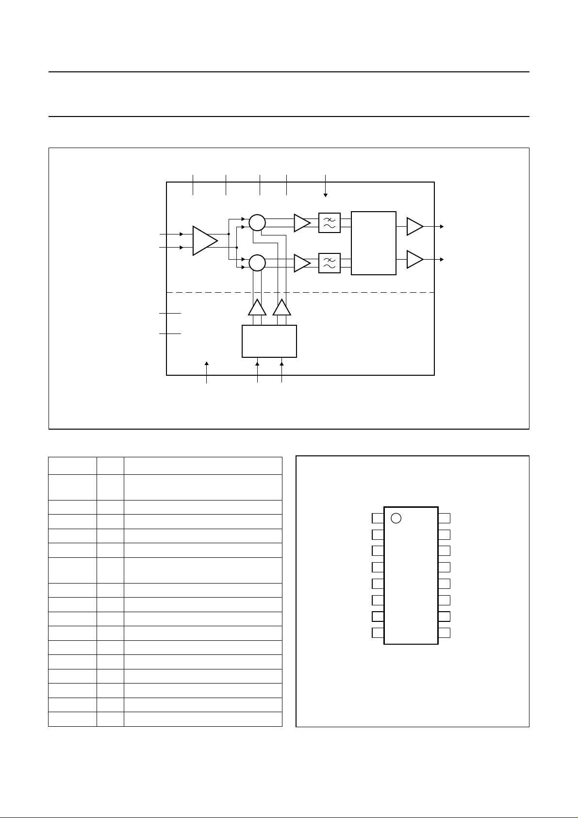
BLOCK DIAGRAM
V
handbook, full pagewidth
CCLNA
LNAGND
GND
n.c.
RXON
1 6
RFINA
RFINB
3
LNA
4
×
×
V
CCLO
LOGND
PINNING
SYMBOL PIN DESCRIPTION
V
CCLNA
1 supply voltage for receive section
(LNA and IF parts)
n.c. 2 not connected
RFINA 3 RF input A (balanced)
RFINB 4 RF input B (balanced)
n.c. 5 not connected
LNAGND 6 ground for receive section (LNA and
IF parts)
SXON 7 SX mode enable input (see Table 1)
n.c. 8 not connected
GND 9 ground
RXON 10 RX mode enable input (see Table 1)
LOINB 11 LO input B (balanced)
LOINA 12 LO input A (balanced)
V
CCLO
13 supply voltage for LO section
LOGND 14 ground for LO section
IFA 15 IF output A (balanced)
IFB 16 IF output B (balanced)
13
135
14
7
SXON
°
QUADRATURE
PHASE
SHIFTER
LOINB LOINA
Fig.1 Block diagram.
2, 5, 8
9
45
10
45
°
COMBINER
°
135
RECEIVE SECTION
LOCAL OSCILLATOR SECTION
°
15
IFA
IF
16
IFB
UAA2077TS
11
12
FCA012
handbook, halfpage
V
CCLNA
n.c.
RFINA
RFINB
n.c.
LNAGND
SXON
n.c.
1
2
3
4
UAA2077TS
5
6
7
8
FCA011
16
15
14
13
12
11
10
9
IFB
IFA
LOGND
V
CCLO
LOINA
LOINB
RXON
GND
Fig.2 Pin configuration.
2000 Apr 17 3
Page 4
Philips Semiconductors Preliminary specification
2 GHz image rejecting front-end UAA2077TS
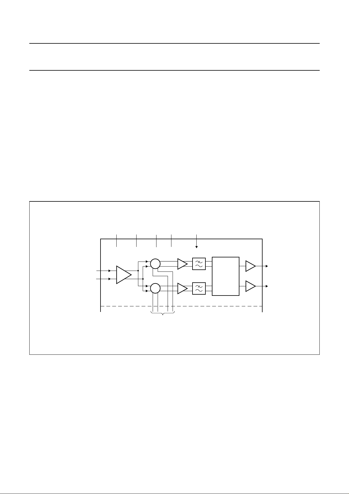
FUNCTIONAL DESCRIPTION
Receive section
The circuit contains a low-noise amplifier followed by two
high dynamic range mixers (see Fig.3). The mixers are of
the Gilbert cell type, the architecture of which is fully
differential.
The LO signal is phase shifted into 45° and 135° signals,
mixed with the RF input signal to provide the
I and Q channel signals. The I and Q channel signals are
buffered, phase shifted by 45° and 135° respectively,
amplified and internally combined, thus obtaining image
rejection.
Balanced signal interfaces are used for minimizing
crosstalk from package parasitics.
handbook, full pagewidth
RFINA
RFINB
CCLNA
3
4
1
LNA
LNAGND
6
GND
9
×
V
×
The IF output is of a differential open collector type.
A typical application consists of pull-up resistors of 680 Ω
at each IF output and a differential load resistance of 1 kΩ
for the IF filter, due to its impedance or its matching
network.
The power gain refers to the resulting power into the 1 kΩ
load. The path for the DC current from VCC into the open
collector outputs should be realized by the inductors.
The output signal is limited to VCC+3VBE.
Fast switching between power-down and the RX mode is
controlled by the mode control pin RXON.
n.c.
2, 5, 8
RXON
10
45°
135°
UAA2077TS
IF
COMBINER
15
IFA
16
IFB
to LO section
Fig.3 Receive section.
2000 Apr 17 4
FCA013
Page 5
Philips Semiconductors Preliminary specification
2 GHz image rejecting front-end UAA2077TS
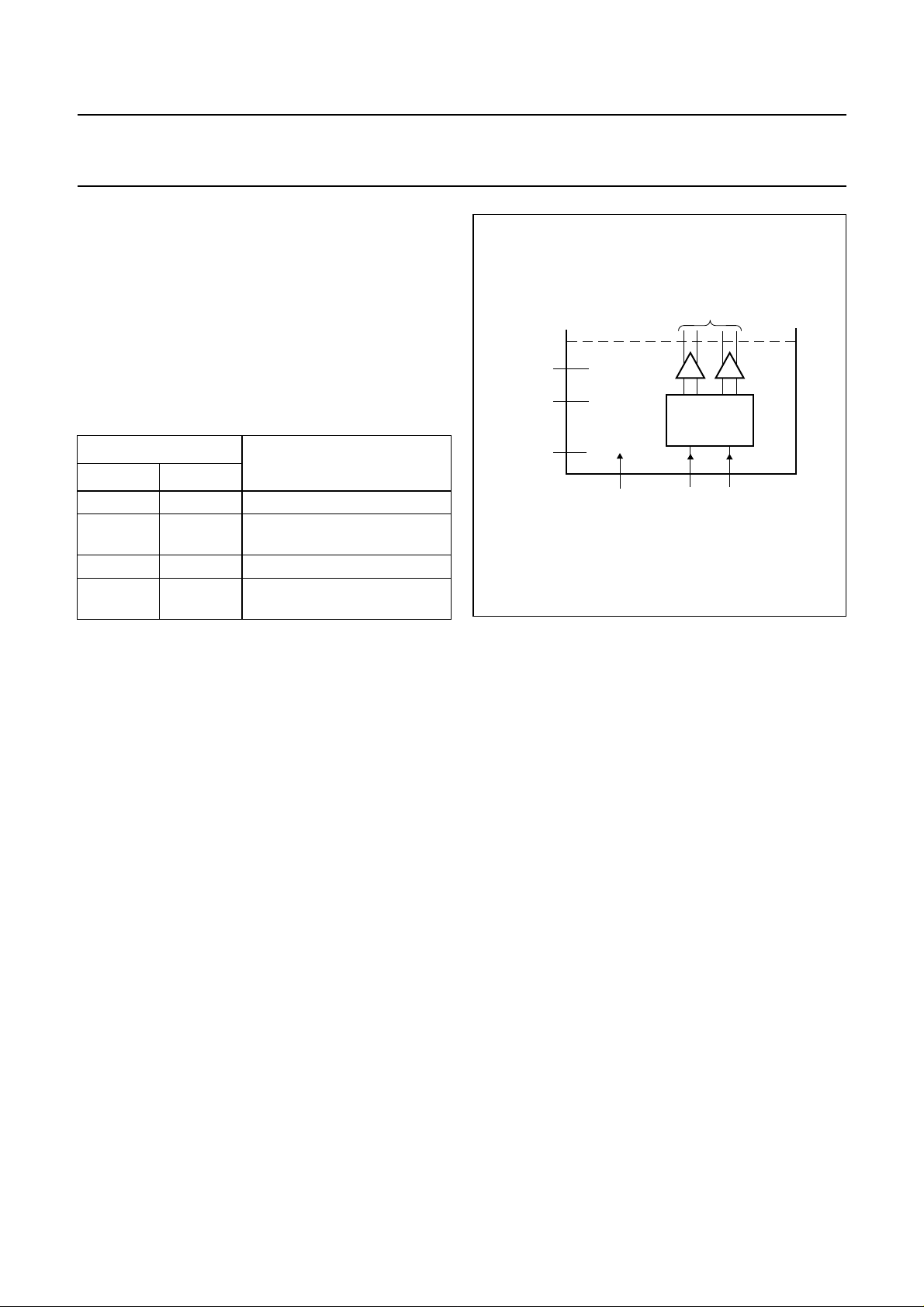
Local oscillator section
The LO input directly drives the two internal all-pass
networks to provide the quadrature signals for the mixers
(see Fig.4).
The SX mode (see Table 1) is used to activate the
LO section, thus minimizingpulling of the external Voltage
Controlled Oscillator (VCO) when enabling the receive
section. The SX mode is active when the logic level on pin
SXON is HIGH.
Table 1 Operating modes
LOGIC LEVEL
MODE
PIN RXON PIN SXON
LOW LOW Power-down mode
HIGH LOW RX mode; receive section
active
LOW HIGH SX mode; LO section active
HIGH HIGH SRX mode; both sections
active
handbook, halfpage
V
CCLO
LOGND
GND
13
14
UAA2077TS
9
7
SXON
Fig.4 LO section.
to receive section
135
°
QUADRATURE
PHASE
SHIFTER
11
LOINB
12
LOINA
45°
FCA014
2000 Apr 17 5
Page 6

Philips Semiconductors Preliminary specification
2 GHz image rejecting front-end UAA2077TS
LIMITING VALUES
In accordance with the Absolute Maximum Rating System (IEC 60134).
SYMBOL PARAMETER CONDITIONS MIN. MAX. UNIT
V
CC
∆V
SS
P
i(max)
T
j(max)
P
tot
T
stg
HANDLING
supply voltage − 6V
difference in voltage between ground pins − 0.6 V
maximum input power − 20 dBm
maximum junction temperature − +150 °C
total power dissipation in free air − 250 mW
storage temperature −65 +150 °C
All pins withstand 1500 V ESD test in accordance with
“MIL-STD-883C class 1 (method 3015.5)”
.
THERMAL CHARACTERISTICS
SYMBOL PARAMETER CONDITIONS VALUE UNIT
R
th(j-a)
thermal resistance from junction to ambient in free air 120 K/W
DC CHARACTERISTICS
V
CC
= 2.8 V; T
=25°C; unless otherwise specified.
amb
SYMBOL PARAMETER CONDITIONS MIN. TYP. MAX. UNIT
Supplies
V
CC
I
CC(pd)
I
CC(RX)
I
CC(SX)
I
CC(SRX)
supply voltage full temperature range 2.7 2.8 3.3 V
power-down supply current −−50 µA
supply current in RX mode − 22 24 mA
supply current in SX mode − 34mA
supply current in SRX mode − 25 28 mA
Mode control: pins RXON and SXON
V
IH
V
IL
I
IH
I
IL
HIGH-level input voltage 1.9 − V
CC
LOW-level input voltage −0.3 − +0.6 V
HIGH-level input current −1 − +1 µA
LOW-level input current −1 − +1 µA
V
2000 Apr 17 6
Page 7

Philips Semiconductors Preliminary specification
2 GHz image rejecting front-end UAA2077TS
AC CHARACTERISTICS
VCC= 2.8 V; T
SYMBOL PARAMETER CONDITIONS MIN. TYP. MAX. UNIT
Receive section (receive section enabled): DCS mode
R
i(RX)
C
i(RX)
f
i(RX)
RL
i(RX)
G
CP(RX)
G
rip
∆G/T gain variation with temperature −60 −30 − mdB/K
CP1
RX
DES3 input referred
IP3
RX
NF
RX
Z
L(RX)
RL
o(RX)
f
o(RX)
IR rejection of image frequency f
Receive section (receive section enabled): PCS mode
R
i(RX)
C
i(RX)
f
i(RX)
RL
i(RX)
G
CP(RX)
G
rip
∆G/T gain variation with temperature −−30 − mdB/K
CP1
RX
=25°C; f
amb
RF input resistance (real part of
= 200 MHz; unless otherwise specified.
o(RX)
balanced; at 1845 MHz − 50 −Ω
the parallel input impedance)
RF input capacitance (imaginary
balanced; at 1845 MHz − 0.5 − pF
part of the parallel input
impedance)
RF input frequency 1805 − 1880 MHz
return loss on matched RF input balanced; note 1 10 15 − dB
conversion power gain RF inputs to IF outputs; note 1 20 23 26 dB
gain ripple as a function of RF
frequency
over DCS frequency range;
note 1
−−1−1.5 dB/100 MHz
1 dB compression point referenced to RF input; note 1 −23.5 −20 − dBm
3 dB desensitisation
interferer frequency offset is
3 MHz; useful signal is
−25 −−dBm
−101 dBm; note 1
3rd order intercept point referenced to RF input; note 1 −15 −12 − dBm
overall noise figure RF inputs to IF outputs; note 1
normal case − 3.5 4.2 dB
typical application IF output load
worsecaseforLO input,power
and V
CC
balanced; note 1 − 1000 −Ω
−−4.4 dB
impedance
return loss on matched IF output note 1 10 15 − dB
IF frequency range fRF>f
RF>fLO
LO
; fRF is the frequency of
− 200 − MHz
30 38 − dB
the wanted signal; note 1
RF input resistance (real part of
balanced; at 1960 MHz − tbf −Ω
the parallel input impedance)
RF input capacitance (imaginary
balanced; at 1960 MHz − tbf − pF
part of the parallel input
impedance)
RF input frequency 1930 − 1990 MHz
return loss on matched RF input balanced; note 1 10 15 − dB
conversion power gain RF inputs to IF outputs; note 1 − 22 − dB
gain ripple as a function of
RF frequency
over PCS frequency range;
note 1
−−1−dB/100 MHz
1 dB compression point referenced to RF input; note 1 −−20 − dBm
2000 Apr 17 7
Page 8

Philips Semiconductors Preliminary specification
2 GHz image rejecting front-end UAA2077TS
SYMBOL PARAMETER CONDITIONS MIN. TYP. MAX. UNIT
DES3 input referred
3 dB desensitisation
IP3
NF
Z
L(RX)
RX
RX
3rd order intercept point referenced to RF input; note 1 −−12 − dBm
overall noise figure R inputs to IF outputs; note 1 − 3.7 − dB
typical application IF output load
impedance
RL
f
o(RX)
o(RX)
return loss on matched IF output note 1 10 15 − dB
IF frequency range fRF>f
IR rejection of image frequency f
Local oscillator section (receive section enabled)
f
i(LO)
R
i(LO)
LO input frequency 1605 − 1790 MHz
LO input resistance (real part of
the parallel input impedance)
C
i(LO)
LO input capacitance (imaginary
part of the parallel input
impedance)
RL
i(LO)
return loss on matched input
(including standby mode)
P
RI
i(LO)
(LO)
LO power level note 1 −10 −3 0 dBm
reverse isolation pins LOIN to RFIN at
Timing
t
stu
start-up time of each block 1 5 20 µs
Notes
1. Measured and guaranteed only on demonstration board including PCB and balun.
interferer frequency offset is
− tbf − dBm
3 MHz; useful signal is
−101 dBm; note 1
balanced; note 1 − 1000 −Ω
LO
RF>fLO
; fRFis the frequency of
− 200 − MHz
− 38 − dB
the wanted signal; note 1
balanced; at 1645 MHz − 50 −Ω
balanced; at 1645 MHz − 1.2 − pF
note 1 10 15 − dB
40 −−dB
LO frequency; note 1
2000 Apr 17 8
Page 9

Philips Semiconductors Preliminary specification
2 GHz image rejecting front-end UAA2077TS
PACKAGE OUTLINE
SSOP16: plastic shrink small outline package; 16 leads; body width 4.4 mm
SOT369-1
D
c
y
Z
16
pin 1 index
9
18
w M
b
e
p
E
H
E
A
2
A
1
L
detail X
A
X
v M
A
Q
(A )
L
p
A
3
θ
0 2.5 5 mm
scale
DIMENSIONS (mm are the original dimensions)
UNIT A1A2A
Note
1. Plastic or metal protrusions of 0.20 mm maximum per side are not included.
A
max.
0.15
mm
1.5
OUTLINE
VERSION
SOT369-1 MO-152
0.00
1.4
1.2
IEC JEDEC EIAJ
0.25
b
3
p
0.32
0.20
0.25
0.13
(1)E(1)
cD
5.30
5.10
REFERENCES
4.5
4.3
0.65
2000 Apr 17 9
eHELLpQZywv θ
1.0
0.75
0.45
0.65
0.45
PROJECTION
0.130.2 0.1
EUROPEAN
6.6
6.2
(1)
0.48
0.18
ISSUE DATE
95-02-04
99-12-27
o
10
o
0
Page 10

Philips Semiconductors Preliminary specification
2 GHz image rejecting front-end UAA2077TS
SOLDERING
Introduction to soldering surface mount packages
Thistextgives a very brief insight toacomplextechnology.
A more in-depth account of soldering ICs can be found in
our
“Data Handbook IC26; Integrated Circuit Packages”
(document order number 9398 652 90011).
There is no soldering method that is ideal for all surface
mount IC packages. Wave soldering is not always suitable
for surface mount ICs, or for printed-circuit boards with
high population densities. In these situations reflow
soldering is often used.
Reflow soldering
Reflow soldering requires solder paste (a suspension of
fine solder particles, flux and binding agent) to be applied
tothe printed-circuit board byscreenprinting, stencilling or
pressure-syringe dispensing before package placement.
Several methods exist for reflowing; for example,
infrared/convection heating in a conveyor type oven.
Throughput times (preheating,soldering and cooling) vary
between 100 and 200 seconds depending on heating
method.
Typical reflow peak temperatures range from
215 to 250 °C. The top-surface temperature of the
packages should preferable be kept below 230 °C.
• Use a double-wave soldering method comprising a
turbulent wave with high upward pressure followed by a
smooth laminar wave.
• For packages with leads on two sides and a pitch (e):
– larger than or equal to 1.27 mm, the footprint
longitudinal axis is preferred to be parallel to the
transport direction of the printed-circuit board;
– smaller than 1.27 mm, the footprint longitudinal axis
must be parallel to the transport direction of the
printed-circuit board.
The footprint must incorporate solder thieves at the
downstream end.
• Forpackageswith leads on four sides, the footprint must
be placed at a 45° angle to the transport direction of the
printed-circuit board. The footprint must incorporate
solder thieves downstream and at the side corners.
During placement andbefore soldering, the package must
be fixed with a droplet of adhesive. The adhesive can be
applied by screen printing, pin transfer or syringe
dispensing. The package can be soldered after the
adhesive is cured.
Typical dwell time is 4 seconds at 250 °C.
A mildly-activated flux will eliminate the need for removal
of corrosive residues in most applications.
Manual soldering
Wave soldering
Conventional single wave soldering is not recommended
forsurfacemount devices (SMDs) or printed-circuit boards
with a high component density, as solder bridging and
non-wetting can present major problems.
To overcome these problems the double-wave soldering
method was specifically developed.
If wave soldering is used the following conditions must be
observed for optimal results:
Fix the component by first soldering two
diagonally-opposite end leads. Use a low voltage (24 V or
less) soldering iron applied to the flat part of the lead.
Contact time must be limited to 10 seconds at up to
300 °C.
When using a dedicated tool, all other leads can be
soldered in one operation within 2 to 5 seconds between
270 and 320 °C.
2000 Apr 17 10
Page 11

Philips Semiconductors Preliminary specification
2 GHz image rejecting front-end UAA2077TS
Suitability of surface mount IC packages for wave and reflow soldering methods
PACKAGE
WAVE REFLOW
(1)
BGA, LFBGA, SQFP, TFBGA not suitable suitable
SOLDERING METHOD
HBCC, HLQFP, HSQFP, HSOP, HTQFP, HTSSOP, SMS not suitable
(3)
PLCC
, SO, SOJ suitable suitable
LQFP, QFP, TQFP not recommended
SSOP, TSSOP, VSO not recommended
(2)
(3)(4)
(5)
suitable
suitable
suitable
Notes
1. All surface mount (SMD) packages are moisture sensitive. Depending upon the moisture content, the maximum
temperature (with respect to time) and body size of the package, there is a risk that internal or external package
cracks may occur due to vaporization of the moisture in them (the so called popcorn effect). For details, refer to the
Drypack information in the
“Data Handbook IC26; Integrated Circuit Packages; Section: Packing Methods”
.
2. These packages are not suitable for wave soldering as a solder joint between the printed-circuit board and heatsink
(at bottom version) can not be achieved, and as solder may stick to the heatsink (on top version).
3. If wave soldering is considered, then the package must be placed at a 45° angle to the solder wave direction.
The package footprint must incorporate solder thieves downstream and at the side corners.
4. Wave soldering is only suitable for LQFP, TQFP and QFP packages with a pitch (e) equal to or larger than 0.8 mm;
it is definitely not suitable for packages with a pitch (e) equal to or smaller than 0.65 mm.
5. Wave soldering is only suitable for SSOP and TSSOP packages with a pitch (e) equal to or larger than 0.65 mm; it is
definitely not suitable for packages with a pitch (e) equal to or smaller than 0.5 mm.
2000 Apr 17 11
Page 12

Philips Semiconductors Preliminary specification
2 GHz image rejecting front-end UAA2077TS
DATA SHEET STATUS
DATA SHEET STATUS
Objective specification Development This data sheet contains the design target or goal specifications for
Preliminary specification Qualification This data sheet contains preliminary data, and supplementary data will be
Product specification Production This data sheet contains final specifications. Philips Semiconductors
Note
1. Please consult the most recently issued data sheet before initiating or completing a design.
DEFINITIONS
Short-form specification The data in a short-form
specification is extracted from a full data sheet with the
same type number and title. For detailed information see
the relevant data sheet or data handbook.
Limiting values definition Limiting values givenare in
accordance with the Absolute Maximum Rating System
(IEC 60134). Stress above one or more of the limiting
values may cause permanent damage to the device.
These are stress ratings only and operation of the device
attheseor at any other conditionsabovethosegiven in the
Characteristics sections of the specification is not implied.
Exposure to limiting values for extended periods may
affect device reliability.
Application information Applications that are
described herein for any of these products are for
illustrative purposes only. Philips Semiconductors make
norepresentationorwarrantythat such applications will be
suitable for the specified use without further testing or
modification.
PRODUCT
STATUS
DEFINITIONS
product development. Specification may change in any manner without
notice.
published at a later date. Philips Semiconductors reserves the right to
make changes at any time without notice in order to improve design and
supply the best possible product.
reserves the right to make changes at any time without notice in order to
improve design and supply the best possible product.
DISCLAIMERS
Life support applications These products are not
designed for use in life support appliances, devices, or
systems where malfunction of these products can
reasonably be expected to result in personal injury. Philips
Semiconductorscustomersusingorsellingthese products
for use in such applications do so at their own risk and
agree to fully indemnify Philips Semiconductors for any
damages resulting from such application.
Right to make changes Philips Semiconductors
reserves the right to make changes, without notice, in the
products, including circuits, standard cells, and/or
software, described or contained herein in order to
improve design and/or performance. Philips
Semiconductors assumes no responsibility or liability for
theuseofany of these products, conveys no licenceortitle
under any patent, copyright, or mask work right to these
products,and makes no representations orwarrantiesthat
these products are free from patent, copyright, or mask
work right infringement, unless otherwise specified.
(1)
2000 Apr 17 12
Page 13

Philips Semiconductors Preliminary specification
2 GHz image rejecting front-end UAA2077TS
NOTES
2000 Apr 17 13
Page 14

Philips Semiconductors Preliminary specification
2 GHz image rejecting front-end UAA2077TS
NOTES
2000 Apr 17 14
Page 15

Philips Semiconductors Preliminary specification
2 GHz image rejecting front-end UAA2077TS
NOTES
2000 Apr 17 15
Page 16

Philips Semiconductors – a w orldwide compan y
Argentina: see South America
Australia: 3 Figtree Drive, HOMEBUSH, NSW 2140,
Tel. +61 2 9704 8141, Fax. +61 2 9704 8139
Austria: Computerstr. 6, A-1101 WIEN, P.O. Box 213,
Tel. +43 1 60 101 1248, Fax. +43 1 60 101 1210
Belarus: Hotel Minsk Business Center, Bld. 3, r. 1211, Volodarski Str. 6,
220050 MINSK, Tel. +375 172 20 0733, Fax. +375 172 20 0773
Belgium: see The Netherlands
Brazil: see South America
Bulgaria: Philips Bulgaria Ltd., Energoproject, 15th floor,
51 James Bourchier Blvd., 1407 SOFIA,
Tel. +359 2 68 9211, Fax. +359 2 68 9102
Canada: PHILIPS SEMICONDUCTORS/COMPONENTS,
Tel. +1 800 234 7381, Fax. +1 800 943 0087
China/Hong Kong: 501 Hong Kong Industrial Technology Centre,
72 Tat Chee Avenue, Kowloon Tong, HONG KONG,
Tel. +852 2319 7888, Fax. +852 2319 7700
Colombia: see South America
Czech Republic: see Austria
Denmark: Sydhavnsgade 23, 1780 COPENHAGEN V,
Tel. +45 33 29 3333, Fax. +45 33 29 3905
Finland: Sinikalliontie 3, FIN-02630 ESPOO,
Tel. +358 9 615 800, Fax. +358 9 6158 0920
France: 51 Rue Carnot, BP317, 92156 SURESNES Cedex,
Tel. +33 1 4099 6161, Fax. +33 1 4099 6427
Germany: Hammerbrookstraße 69, D-20097 HAMBURG,
Tel. +49 40 2353 60, Fax. +49 40 2353 6300
Hungary: see Austria
India: Philips INDIA Ltd, Band Box Building, 2nd floor,
254-D, Dr. Annie Besant Road, Worli, MUMBAI 400 025,
Tel. +91 22 493 8541, Fax. +91 22 493 0966
Indonesia: PT Philips Development Corporation,Semiconductors Division,
Gedung Philips, Jl. Buncit Raya Kav.99-100, JAKARTA 12510,
Tel. +62 21 794 0040 ext. 2501, Fax. +62 21 794 0080
Ireland: Newstead, Clonskeagh, DUBLIN 14,
Tel. +353 1 7640 000, Fax. +353 1 7640 200
Israel: RAPAC Electronics, 7 Kehilat Saloniki St, PO Box 18053,
TEL AVIV 61180, Tel. +972 3 645 0444, Fax. +972 3 649 1007
Italy: PHILIPS SEMICONDUCTORS, Via Casati, 23 - 20052 MONZA (MI),
Tel. +39 039 203 6838, Fax +39 039 203 6800
Japan: Philips Bldg 13-37, Kohnan 2-chome, Minato-ku,
TOKYO 108-8507, Tel. +81 3 3740 5130, Fax. +81 3 3740 5057
Korea: Philips House, 260-199 Itaewon-dong, Yongsan-ku, SEOUL,
Tel. +82 2 709 1412, Fax. +82 2 709 1415
Malaysia: No. 76 Jalan Universiti, 46200 PETALING JAYA, SELANGOR,
Tel. +60 3 750 5214, Fax. +60 3 757 4880
Mexico: 5900 Gateway East, Suite 200, EL PASO, TEXAS 79905,
Tel. +9-5 800 234 7381, Fax +9-5 800 943 0087
Middle East: see Italy
Netherlands: Postbus 90050, 5600 PB EINDHOVEN, Bldg. VB,
Tel. +31 40 27 82785, Fax. +31 40 27 88399
New Zealand: 2 Wagener Place, C.P.O. Box 1041, AUCKLAND,
Tel. +64 9 849 4160, Fax. +64 9 849 7811
Norway: Box 1, Manglerud 0612, OSLO,
Tel. +47 22 74 8000, Fax. +47 22 74 8341
Pakistan: see Singapore
Philippines: Philips Semiconductors Philippines Inc.,
106 Valero St. Salcedo Village, P.O. Box 2108 MCC, MAKATI,
Metro MANILA, Tel. +63 2 816 6380, Fax. +63 2 817 3474
Poland: Al.Jerozolimskie 195 B, 02-222 WARSAW,
Tel. +48 22 5710 000, Fax. +48 22 5710 001
Portugal: see Spain
Romania: see Italy
Russia: Philips Russia, Ul. Usatcheva 35A, 119048 MOSCOW,
Tel. +7 095 755 6918, Fax. +7 095 755 6919
Singapore: Lorong 1, Toa Payoh, SINGAPORE 319762,
Tel. +65 350 2538, Fax. +65 251 6500
Slovakia: see Austria
Slovenia: see Italy
South Africa: S.A. PHILIPS Pty Ltd., 195-215 Main Road Martindale,
2092 JOHANNESBURG, P.O. Box 58088 Newville 2114,
Tel. +27 11 471 5401, Fax. +27 11 471 5398
South America: Al. Vicente Pinzon, 173, 6th floor,
04547-130 SÃO PAULO, SP, Brazil,
Tel. +55 11 821 2333, Fax. +55 11 821 2382
Spain: Balmes 22, 08007 BARCELONA,
Tel. +34 93 301 6312, Fax. +34 93 301 4107
Sweden: Kottbygatan 7, Akalla, S-16485 STOCKHOLM,
Tel. +46 8 5985 2000, Fax. +46 8 5985 2745
Switzerland: Allmendstrasse 140, CH-8027 ZÜRICH,
Tel. +41 1 488 2741 Fax. +41 1 488 3263
Taiwan: Philips Semiconductors, 6F, No. 96, Chien Kuo N. Rd., Sec. 1,
TAIPEI, Taiwan Tel. +886 2 2134 2886, Fax. +886 2 2134 2874
Thailand: PHILIPS ELECTRONICS (THAILAND) Ltd.,
209/2 Sanpavuth-Bangna Road Prakanong, BANGKOK 10260,
Tel. +66 2 745 4090, Fax. +66 2 398 0793
Turkey: Yukari Dudullu, Org. San. Blg., 2.Cad. Nr. 28 81260 Umraniye,
ISTANBUL, Tel. +90 216 522 1500, Fax. +90 216 522 1813
Ukraine: PHILIPS UKRAINE, 4 Patrice Lumumba str., Building B, Floor 7,
252042 KIEV, Tel. +380 44 264 2776, Fax. +380 44 268 0461
United Kingdom: Philips Semiconductors Ltd., 276 Bath Road, Hayes,
MIDDLESEX UB3 5BX, Tel. +44 208 730 5000, Fax. +44 208 754 8421
United States: 811 East Arques Avenue, SUNNYVALE, CA 94088-3409,
Tel. +1 800 234 7381, Fax. +1 800 943 0087
Uruguay: see South America
Vietnam: see Singapore
Yugoslavia: PHILIPS, Trg N. Pasica 5/v, 11000 BEOGRAD,
Tel. +381 11 3341 299, Fax.+381 11 3342 553
For all other countries apply to: Philips Semiconductors,
International Marketing & Sales Communications, Building BE-p, P.O. Box 218,
5600 MD EINDHOVEN, The Netherlands, Fax. +31 40 27 24825
© Philips Electronics N.V. SCA
All rights are reserved. Reproduction in whole or in part is prohibited without the prior written consent of the copyright owner.
The information presented in this document does not form part of any quotation or contract, is believed to be accurate and reliable and may be changed
without notice. No liability will be accepted by the publisher for any consequence of its use. Publication thereof does not convey nor imply any license
under patent- or other industrial or intellectual property rights.
2000
Internet: http://www.semiconductors.philips.com
69
Printed in The Netherlands 403506/02/pp16 Date of release: 2000 Apr 17 Document order number: 9397 750 07033
 Loading...