

Page 1

DATA SH EET
Product specification
Supersedes data of 1995 Sep 18
File under Integrated Circuits, IC17
1996 Oct 22
INTEGRATED CIRCUITS
UAA2067G
Image reject 1800 MHz transceiver
for DECT applications
Page 2

1996 Oct 22 2
Philips Semiconductors Product specification
Image reject 1800 MHz transceiver
for DECT applications
UAA2067G
FEATURES
• Receiver with:
– low noise amplifier
– dual quadrature mixers for image rejection
(lower sideband)
– I and Q combining networks at a fixed IF
• Both high-frequency and low-frequency VCOs including
buffers with good isolation for low pulling
• Transmitter with:
– dual quadrature mixers for image rejection
(lower sideband)
– amplitude ramping circuit
– amplifier with high output power.
APPLICATIONS
• 1800 MHz transceiver for DECT hand-portable
equipment
• TDMA systems.
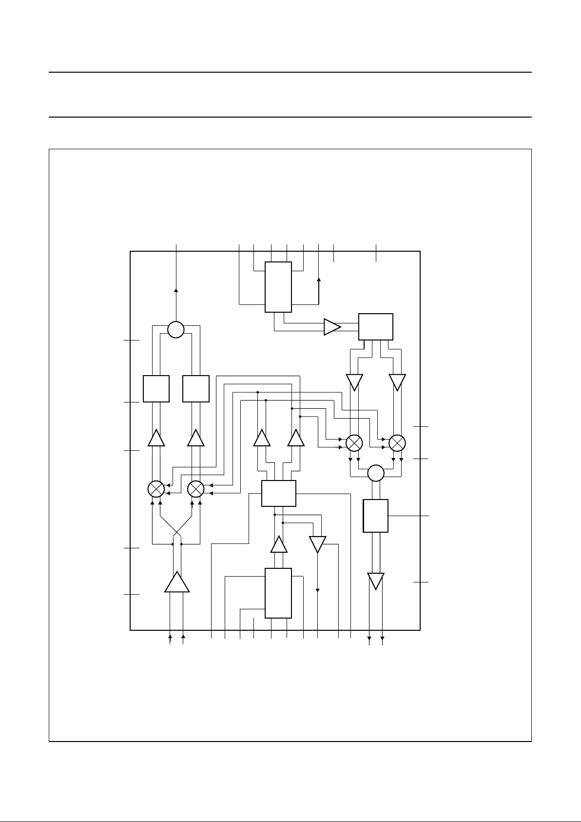
GENERAL DESCRIPTION
The UAA2067G is a low-power transceiver intended for
use in portable and base station transceivers complying
with the DECT system. The IC performs in accordance
with specifications in the −30 to +85°C temperature range.
The UAA2067G contains a front-end receiver for the
1800 to 1900 MHz frequency range, a high-frequency
VCO for the 1650 to 1850 MHz range, a low-frequency
VCO for the 100 to 140 MHz frequency range and a
transmitter with a high-output power amplifier driver stage
for the 1800 to 1900 MHz frequency range. Designed in
an advanced BiCMOS process, it combines high
performance with low-power consumption and a high
degree of integration, thus reducing external component
costs and total radio size.
Its first advantage is to provide typically 34 dB of image
rejection in the receiver path. Thus, the image filter
between the LNA and the mixer is redundant and
consequently can be removed. The receive section
consists of a low-noise amplifier that drives a quadrature
mixer pair. Image rejection is achieved by this RF mixer
pair and the two phase shifters in the I and Q channels that
phase shift the IF by 45° and 135° respectively. The two
phase shifted IFs are recombined and buffered to furnish
the IF output signal.
Signals presented at the RF input at LO − IF frequency are
rejected through this signal processing while signals at
LO + IF frequency can form the IF signal.
Its second advantage is to provide a good buffered
high-frequency VCO signal to the RX and TX mixers and
to the synthesizer-prescaler. Switching the receive or
transmit section on gives a very small change in VCO
frequency.
Its third advantage is to provide a good buffered
low-frequency VCO signal to the TX mixers, to the
synthesizer-prescaler and the second down conversion
mixer in a double conversion receiver. Switching the
transmit section on gives a very small change in
VCO frequency.
The frequency of each VCO is determined by a resonator
network that is external to the IC. Each VCO has a
regulated power supply voltage that has been designed
specifically for minimizing a change in frequency due to
changes in the power supply voltage, which may be
caused for instance by switching on the power amplifier.
Its fourth advantage is to provide typically 33 dBc of image
rejection in the single-sideband up-conversion mixer. Thus
the image filter between the power amplifier and the
antenna is redundant and may consequently be removed.
Image rejection is achieved in the internal architecture by
two RF mixers in quadrature and two phase shifters in the
low-frequency VCO signal that shifts the phase to
0° and 90°. The output signals of the mixers are summed
to form the single-upper-sideband output signal.
The output stage is a high-level output buffer with an
output power of approximately 4 dBm. The output level is
sufficient to drive a three-stage bipolar preamplifier
for DECT.
ORDERING INFORMATION
TYPE NUMBER
PACKAGE
NAME DESCRIPTION VERSION
UAA2067G LQFP32 plastic low profile quad flat package; 32 leads; body 5 × 5 × 1.4 mm SOT401-1
Page 3

1996 Oct 22 3
Philips Semiconductors Product specification
Image reject 1800 MHz transceiver
for DECT applications
UAA2067G
QUICK REFERENCE DATA
For conditions see Chapters “DC characteristics” and “AC characteristics”.
SYMBOL PARAMETER MIN. TYP. MAX. UNIT
V
CC
supply voltage 3.0 3.6 5.5 V
I
CC(RX)
receive supply current − 24 − mA
I
CC(TX)
transmit supply current − 42 − mA
I
CC(RFLO)
RF oscillator supply current − 15 − mA
I
CC(IFLO)
IF oscillator supply current − 7 − mA
NF
RX
receive noise figure −−7.0 dB
G
CP
conversion power gain − 30 − dB
IR
RX
receive image frequency rejection − 34 − dB
f
RFLO
RFLO frequency range 1.65 − 1.85 GHz
f
IFLO
IFLO frequency range 100 − 140 MHz
P
out
output transmit power − 4 − dBm
IR
TX
transmit image frequency rejection − 33 − dBc
T
amb
operating ambient temperature −30 +25 +85 °C
Page 4
1996 Oct 22 4
Philips Semiconductors Product specification
Image reject 1800 MHz transceiver
for DECT applications
UAA2067G
BLOCK DIAGRAM
handbook, full pagewidth
0
o
90
o
45
o
135
o
RFLO
OSCILLATOR
0
o
90
o
5
1
6
7
2
4
UAA2067
3
8
14
MGC867
11109
12
13
19
16
17
24
21
20
15
22
23
18
29
28
32 27 31
PDRX
GND6
V
CC(MIX)
V
CC1(RFLO)
V
CC2(RFLO)
V
CC(RFLOO)
GND4
GND5
RFLOA
RFLOB
RFLOREG
V
CC(TX)
GND3
GND7
RXA
RXB
TXA
TXB
PDTX TXRAMP
PDRFLO
RFLOO
V
CC(IFLO)
GND2
GND1
IFLORES
IFLOREG
PDIFLO
IFLOO
ICEN
IFDEC
IFO
30 26
25
IFLO
OSCILLATOR
LNA
RAMP
∑
∑
Fig.1 Block diagram.
Page 5

1996 Oct 22 5
Philips Semiconductors Product specification
Image reject 1800 MHz transceiver
for DECT applications
UAA2067G
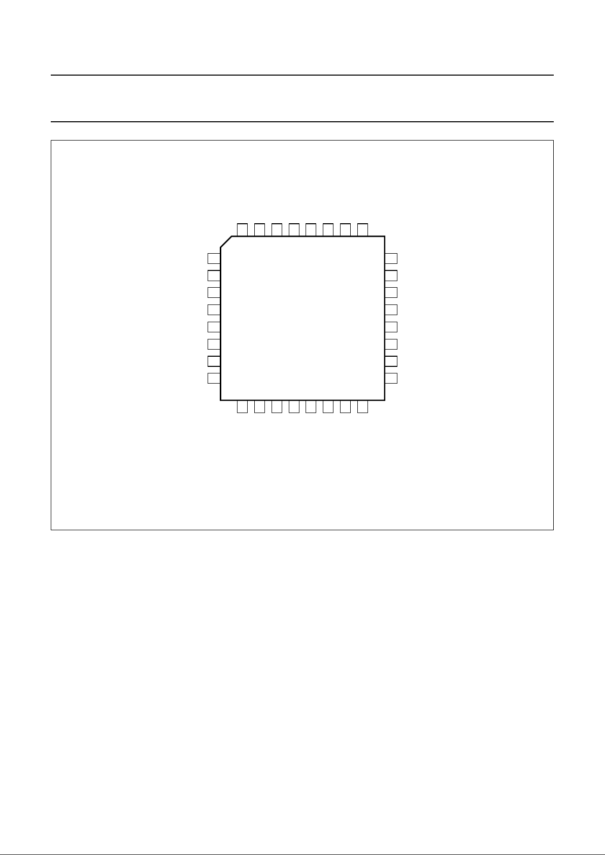
PINNING
Notes
1. Pins 3 and 7 are internally short-circuited.
2. Pins 11 and 27 should be at the same DC voltage.
3. Pins 18 and 23 are internally short-circuited.
4. Pins 19 and 22 are internally short-circuited.
SYMBOL PIN DESCRIPTION
PDIFLO 1 power-down for IFLO
IFLOREG 2 regulator decoupling for IFLO
GND1 3 ground for IFLO; note 1
IFLOO 4 IFLO output
V
CC(IFLO)
5 supply voltage for IFLO
IFLORES 6 IFLO resonator
GND2 7 ground for IFLO resonator; note 1
ICEN 8 IC enable
PDTX 9 power-down for transmitter
TXRAMP 10 power ramping transmitter
V
CC(TX)
11 supply voltage for transmitter output stage; note 2
TXB 12 transmitter RF output B
TXA 13 transmitter RF output A
GND3 14 ground for transmitter output stage
PDRFLO 15 power-down for RFLO
V
CC(RFLOO)
16 supply voltage for RFLO output
RFLOO 17 RFLO output
V
CC1(RFLO)
18 supply voltage for RFLO oscillator; note 3
GND4 19 ground for RFLO oscillator; note 4
RFLOA 20 RFLO resonator
RFLOB 21 RFLO resonator
GND5 22 ground for RFLO oscillator; note 4
V
CC2(RFLO)
23 supply voltage for RFLO oscillator; note 3
RFLOREG 24 regulator decoupling for RFLO
IFO 25 receiver IF output
IFDEC 26 IF decoupling
V
CC(MIX)
27 supply voltage for receive and transmit mixers; note 2
RXA 28 receiver RF input A
RXB 29 receiver RF input B
GND6 30 ground for receive and transmit mixers
PDRX 31 power-down for receiver
GND7 32 die-pad ground
Page 6
1996 Oct 22 6
Philips Semiconductors Product specification
Image reject 1800 MHz transceiver
for DECT applications
UAA2067G
Fig.2 Pin configuration.
handbook, full pagewidth
UAA2067
MGC865
1
2
3
4
5
6
7
8
PDIFLO
IFLOREG
GND1
IFLOO
V
CC(IFLO)
IFLORES
GND2
ICEN
RFLOREG
V
CC2(RFLO)
GND5
RFLOB
RFLOA
GND4
V
CC1(RFLO)
RFLOO
24
23
22
21
20
19
18
17
9
10
11
12
13
14
15
16
PDTX
TXRAMP
V
CC(TX)
TXB
TXA
GND3
PDRFLO
V
CC(RFLOO)
32
31
30
29
28
27
26
25
GND7
PDRX
GND6
RXB
RXA
V
CC(MIX)
IFDEC
IFO
Page 7

1996 Oct 22 7
Philips Semiconductors Product specification
Image reject 1800 MHz transceiver
for DECT applications
UAA2067G
FUNCTIONAL DESCRIPTION
Receive section
The circuit contains a balanced low-noise amplifier
followed by two high dynamic range mixers. The local
oscillator signals, shifted in phase to 0 and 90° mix the
amplified RF signal to the I and Q channels.These two
channels are buffered, phase shifted by 45° and 135°
respectively, amplified and recombined internally to realize
the image rejection. Signals at the RF input at RFLO − IF
frequencies are rejected through the signal processing
while signals at the RFLO + IF frequencies form the
IF signals.
An image rejection of typically 34 dB is obtained for an IF
between 100 and 120 MHz.
Balanced signals are used for minimizing crosstalk due to
package parasitics. The IF output is single-ended.
The typical load is 50 Ω.
Fast switching, on/off of the receive section is controlled
by the hardware input PDRX.
RFLO section
The high-frequency oscillator (RFLO oscillator) supplies
the local oscillator signal for the down-conversion (receive)
and up-conversion (transmit) mixers. This VCO uses an
on-chip regulator for a power-supply voltage-independent
output frequency. The buffered VCO signal is fed into a
phase shifter and an off-chip prescaler-synthesizer.
The output signal of the phase-shifter is used for driving
the RX and TX mixers. Due to the good isolation in the
buffer stages, a very small change in VCO frequency is
obtained when switching the RX and TX mixers on.
Fast switching, on/off of the oscillator section is controlled
by the hardware input PDRFLO.
IFLO section
The low-frequency oscillator (IFLO oscillator) internally
supplies the local oscillator signal to the single-sideband
transmit mixer. The buffered VCO signal is fed into a
phase shifter. The output signal of the phase-shifter is
used for driving the TX mixers.
Due to the good isolation in the buffer stages, a very small
change in VCO frequency is obtained when switching the
TX mixer on.
Fast switching on/off of the oscillator section is controlled
by the hardware input PDIFLO input.
Transmit section
The circuit contains two balanced mixers, each of which is
driven by the RFLO and IFLO signals. The output signal of
the two mixers is summed and buffered to obtain the single
upper-sideband signal at frequency RFLO + IFLO.
With the use of an off-chip time constant, the ramping
circuit defines the power ramp-up and ramp-down of the
pre-amplifier output signal.
Balanced signals are used for minimizing crosstalk due to
package parasitics.
Fast switching, on/off, of the transmit section is controlled
by the hardware input PDTX.
The power supply voltage of the transmit mixers, the
adding circuit and ramping circuit is taken from the
V
CC(MIX)
and GND6 for maximum isolation from the
preamplifier output stage.
OPERATING MODES
To use the IC, all V
CC
pins must be connected to the
supply voltage.
For transceiving a DECT signal, the RFLO and IFLO
sections should be powered-on. After a stable frequency
has been reached (mainly determined by the synthesizer
design), the receiver or transmitter can be powered-on.
GMSK data modulation can be supplied in two different
ways: the data is directly modulated on IFLO or RFLO.
The ramping of the power level can be set with a time
constant that is external to the IC.
Table 1 gives the definition of the polarity of the switching
signals on the receive, the RFLO, the IFLO and the
transmit sections.
Page 8
1996 Oct 22 8
Philips Semiconductors Product specification
Image reject 1800 MHz transceiver
for DECT applications
UAA2067G
Table 1 Switching signals on the receiver
Note
1. Active when ICEN is enabled.
LIMITING VALUES
In accordance with the Absolute Maximum Rating System (IEC 134).
Note
1. Pins short-circuited internally must be short-circuited externally.
THERMAL CHARACTERISTICS
HANDLING
Every pin withstands the ESD test in accordance with
“MIL-STD-883C class 2 (method 3015.5)”
.
SIGNAL SECTION LEVEL on/off
PDRX receive section powered-on LOW on
(1)
receive section powered-off HIGH off
PDRFLO RFLO section powered-on LOW on
(1)
RFLO section powered-off HIGH off
PDIFLO IFLO section powered-on LOW on
(1)
IFLO section powered-off HIGH off
PDTX transmit section powered-on LOW on
(1)
transmit section powered-off HIGH off
ICEN all sections disabled LOW off
all sections enabled HIGH on
SYMBOL PARAMETER CONDITIONS MIN. MAX. UNIT
V
CC
supply voltage − 6V
∆GND difference in ground supply voltage applied
between all grounds
note 1 − + 0.3 V
P
l(max)
maximum power input − +20 dBm
T
j(max)
maximum operating junction temperature − +150 °C
P
dis(max)
maximum power dissipation in stagnant air at 25°C − 500 mW
T
stg
storage temperature −65 +150 °C
SYMBOL PARAMETER VALUE UNIT
R
th j-a
thermal resistance from junction to ambient in free air 90 K/W
Page 9

1996 Oct 22 9
Philips Semiconductors Product specification
Image reject 1800 MHz transceiver
for DECT applications
UAA2067G
DC CHARACTERISTICS
V
CC
= 3.6 V; T
amb
=25°C; unless otherwise specified.
SYMBOL PARAMETER CONDITIONS MIN. TYP. MAX. UNIT
Pins: V
CC(MIX)
, V
CC(TX)
, V
CC(IFLO)
, V
CC1(RFLO)
, V
CC2(RFLO)
and V
CC(RFLOO)
V
CC
supply voltage over full temperature range 3.0 3.6 5.5 V
I
CC(RX)
supply current receive section on; DC tested 18 24 30 mA
I
CC(RFLO)
supply current RFLO RFLO section on; DC tested 11 15 20 mA
I
CC(IFLO)
supply current IFLO IFLO section on; DC tested 5 7 9 mA
I
CC(TX)
supply current transmit section on; DC tested 34 42 54 mA
I
CC(PD)
supply current power-down mode; DC tested − 250 µA
Pins: PDRX, PDTX, PDRFLO, PDIFLO and ICEN
V
IH
HIGH level input voltage 2.1 − VCC+ 0.3 V
V
IL
LOW level input voltage −0.3 − 0.8 V
I
IH
HIGH level static input current pin at VCC− 0.4 V −1 − +1 µA
I
IL
LOW level static input current pin at 0.4 V −1 − +1 µA
Pins: RXA, RXB, IFO and IFDEC
V
RXA,B
DC input voltage level receive section on 2.1 2.4 2.7 V
V
IFO
DC output voltage level receive section on 0.9 1.1 1.3 V
V
IFDEC
DC level receive section on 2.45 2.65 2.85 V
Pins: RFLOA, RFLOB, RFLOREG and RFLOO
I
RFLOA,B
DC current RFLO section on 123 mA
V
RFLOREG
DC level RFLO section on 2.45 2.65 2.85 V
V
RFLOO
DC output voltage level RFLO section on 2.8 3.1 3.4 V
Pins: IFLORES, IFLOREG and IFLOO
V
IFLORES
DC level IFLO section on 1.85 2.1 2.3 V
V
IFLOREG
DC level IFLO section on 2.35 2.55 2.8 V
V
IFLOO
DC output voltage level IFLO section on 2.2 2.45 2.7 V
Pins: TXA, TXB and TXRAMP
I
TXA,B
DC output current transmit section on 21018 mA
I
TXRAMP
DC input current V
TXRAMP
=3V;
transmit section on
−−200 µA
Page 10

1996 Oct 22 10
Philips Semiconductors Product specification
Image reject 1800 MHz transceiver
for DECT applications
UAA2067G
AC CHARACTERISTICS
V
CC
= 3.0 to 5.5 V; T
amb
= −30 to +85°C; unless otherwise specified.
SYMBOL PARAMETER CONDITIONS MIN. TYP. MAX. UNIT
Receive mode (receive and RFLO sections powered-on)
f
RFI
RF input frequency 1800 − 1900 MHz
R
iRF
RF input resistance
(real part of the parallel input
impedance)
balanced; at 1890 MHz − 190 −Ω
C
iRF
RF input capacitance (imaginary
part of the parallel input
impedance)
balanced; at 1890 MHz − 0.8 − pF
PRFLO
RX
RFLO level at input to RX balun note 1 −−70 −40 dBm
DES3
RX
RF interference for 3 dB
desensitization
interference frequency offset
6 MHz; note 1
−−35 − dBm
G
CP
conversion power gain RF input to IF output
(typical load)
over full temperature range 24 30 36 dB
T
amb
=25°C273033dB
CP1
RX
1 dB input compression point referenced to RF input; note 1 −36 −33 − dBm
P
o(RX)
IF power for
CP1RX<Pin< +8 dBm
referenced to IF power at
CP1RX; note 1
−6 − +6 dB
t
rec
recovery time for Pin= +12 dBm note 1 − 230µs
IP2-2
RX
mixer 2-2 spurious intercept point referenced to the RF input;
note 1
−6+2 − dBm
IP3
RX
3rd order intercept point referenced to the RF input;
note 1
−30 −25 − dBm
NF
RX
overall noise figure RF input to IF output; note 1 − 5.8 7 dB
f
IF
IF frequency range 100 110 120 MHz
Z
L(IF)
typical application IF output load
impedance
fIF = 110 MHz − 50 −Ω
IR
RX
image frequency rejection over full temperature range 20 34 − dB
T
amb
=25°C2334−dB
PSRR power supply rejection ratio note 1; typical load; at 110 MHz 35 −−dB
Page 11

1996 Oct 22 11
Philips Semiconductors Product specification
Image reject 1800 MHz transceiver
for DECT applications
UAA2067G
RF local oscillator (RFLO section powered-on)
f
RFLO(min)
minimum oscillator frequency
range
1650 − 1850 MHz
R
i(RFLO)
oscillator input resistance (real
part of the parallel input
impedance)
balanced; at 1.77 GHz −−250 −Ω
C
i(RFLO)
oscillator input capacitance
(imaginary part of the parallel
input impedance)
balanced; at 1.77 GHz − 2.7 − pF
V
o(RFLO)
local oscillator output level at
pin 17; RMS value
note 2; typical load resistance 50 75 − mV
Z
o(RFLO)
local oscillator output impedance
at pin 17
at 1.77 GHz − 30 − 60j −Ω
R
L(RFLO)
typical load resistance − 300 −Ω
HAR
(RFLO)
harmonic levels at RFLO output
(pin 17)
note 1 −− −20 dBc
IF local oscillator (IFLO section powered-on)
f
IFLO(min)
minimum oscillator frequency
range
100 120 140 MHz
R
i(IFLO)
oscillator input resistance
(real part of the parallel input
impedance)
−−480 −Ω
C
i(IFLO)
oscillator input capacitance
(imaginary part of the parallel
input impedance)
− 2.1 − pF
V
o(IFLO)
IF local oscillator output level at
pin 4; RMS value
100 160 − mV
Z
o(IFLO)
local oscillator output impedance
(real part)
−− 100 Ω
R
L(IFLO)
typical load resistance − 5 − kΩ
C
L(IFLO)
typical load capacitance − 7 − pF
HAR
(IFLO)
harmonic levels at IFLO output note 1 −− −15 dBc
SYMBOL PARAMETER CONDITIONS MIN. TYP. MAX. UNIT
Page 12

1996 Oct 22 12
Philips Semiconductors Product specification
Image reject 1800 MHz transceiver
for DECT applications
UAA2067G
Notes
1. Measured and guaranteed only on the Philips demonstration board, including PCB and balun.
2. The imaginary part of the load impedance has been tuned out. A power match is assumed.
3. A simplified DECT type approval measurement is used; the spectrum analyser has the following settings:
RBW = 100 kHz, VBW = 100 Hz, use delta marker and add 50 dB (correction for RBW = 100 kHz), f
RFLO
= 1.77 GHz
and f
IFLO
= 120 MHz, ∆f = 4.686 MHz.
Transmit mode (transmit, RFLO and IFLO sections powered-on)
f
TX
RF output frequency 1800 − 1900 MHz
R
o(TX)
RF output resistance (real part of
the parallel output impedance)
balanced; note 1 − 110 −Ω
C
o(TX)
RF output capacitance (imaginary
part of the parallel output
impedance)
balanced; note 1 − 0.6 − pF
FTRFLO
TX
RFLO feedthrough at the TX
output
referenced to the desired
frequency; T
amb
=25°C; note 1
−−25 −23 dBc
Pout output transmit power V
TXRAMP
= 0 V; note 1
over full temperature range −2 4 8 dBm
T
amb
=25°C 1 4 7 dBm
IR
TX
image frequency rejection referenced to the desired
frequency; note 1
over full temperature range 20 33 − dBc
T
amb
=25°C2333−dBc
Z
inTXRAMP
input impedance at pin TXRAMP 10 −−kΩ
C
inTXRAMP
input capacitance at pin TXRAMP −− 10 pF
V
TXRAMP(max)
ramp voltage for P
out=Pmax
− 0V
V
TXRAMP(min)
ramp voltage for
P
out=Pmax
− 30 dB
− 3.0 − V
CNR
TX
carrier-to-noise ratio at TX output T
amb
=25°C; notes 1 and 3 +130 +133 − dBc/Hz
Timing
t
up
start-up/power-down time of each
block
over full temperature range − 510µs
C
i
input capacitance of logic inputs over full temperature range −− 5pF
SYMBOL PARAMETER CONDITIONS MIN. TYP. MAX. UNIT
Page 13

1996 Oct 22 13
Philips Semiconductors Product specification
Image reject 1800 MHz transceiver
for DECT applications
UAA2067G
INTERNAL PIN CONFIGURATION
SYMBOL PIN
DC
VOLTAGE
(V)
EQUIVALENT CIRCUIT
PDIFLO 1 −
ICEN 8 −
PDTX 9 −
PDRFLO 15 −
PDRX 31 −
IFLOREG 2 2.55
RFLOREG 24 2.65
IFDEC 26 2.65
GND 3, 7, 14,
19, 22,
30, 32
0
IFLOO 4 2.45
V
CC
5, 11, 16,
18, 23, 27
3.6
IFLORES 6 2.1
MBH672
V
CC
GND
1, 8, 9, 15, 31
MBH673
V
CC
GND
2, 24, 26
MBH674
V
CC(IFLO)
GND
4
MBH675
V
IFLOREG
GND
6
Page 14

1996 Oct 22 14
Philips Semiconductors Product specification
Image reject 1800 MHz transceiver
for DECT applications
UAA2067G
TXRAMP 10 −
TXB 12 V
CC
TXA 13 V
CC
RFLOO 17 3.1
RFLOA 20 2.0
RFLOB 21 2.0
SYMBOL PIN
DC
VOLTAGE
(V)
EQUIVALENT CIRCUIT
MBH676
V
CC(MIX)
V
CC(TX)
GND
10
MBH677
12 13
V
CC(TX)
GND
MBH678
V
CC(RFLOO)
GND
17
MBH679
20 21
V
RFLOREG
GND
Page 15

1996 Oct 22 15
Philips Semiconductors Product specification
Image reject 1800 MHz transceiver
for DECT applications
UAA2067G
IFO 25 1.1
RXA 28 2.4
RXB 29 2.4
SYMBOL PIN
DC
VOLTAGE
(V)
EQUIVALENT CIRCUIT
MBH680
V
CC(IFLO)
GND
25
MBH681
V
CC(MIX)
GND
28
29
Page 16

1996 Oct 22 16
Philips Semiconductors Product specification
Image reject 1800 MHz transceiver
for DECT applications
UAA2067G
APPLICATION INFORMATION
handbook, full pagewidth
mod tune
V
CC
BB515BB515
BBY
5103W
RFLO
output
BBY
5103W
RFLO tune
MGC866
V
CC
R3
4.7 kΩ
R2
10 kΩ
L1
82 nH
C8
150 pF
C6
10 pF
C5
22 nF
C9
4.7 pF
C14
1 nF
C13
10 pF
C7
1 nF
5.6 nH
5.6 nH
12 nH
1 pF
TX
output
1 pF
8.2 pF
8.2
pF
V
CC
1/4
λ
TXRAMP
R4
4.7 kΩ
8.2 nF
PDTX
C11
10 pF
ICEN
C10
10 pF
L6
(0603)
1.5 nH
L7
(0603)
1.5 nH
C25
22 pF
C26
22 pF
C27
10 pF
R8
1 kΩ
R7
1 kΩ
8.2
pF
C28
22 nF
C32
4.7 nF
C31
1 nF
C30
1 nF
C29
10 pF
C1
10 pF
C39
10 pF
C4
1 nF
C2
1 nF
C24
4.7 nF
C23
8.2 pF
C22
10 pF
C19
10 pF
C20
1 nF
C21
10 pF
6.8 nH
6.8 nH
6.8 nH
8.2 pF
8.2 pF
RF
input
IFLO
output
0.82 pF
0.82 pF
1/4
λ
1/4 λ
R5
33 Ω
R6
33 Ω
V
CC
V
CC
V
CC
PDRFLO
UAA2067
C33
10 pF
C34
1 nF
IF
output
PDRX
PDIFLO
24
262527
28
29
30
31
32
78
6
54321
23222120191817
151614
13
12
11
10
9
1/4 λ
Fig.3 Demonstration board diagram.
Figure 3 illustrates the electrical diagram of the UAA2067G Philips demonstration board for DECT applications. All matching is to 50 Ω for measurement purposes.
Different values will be used in a real application.
Page 17

1996 Oct 22 17
Philips Semiconductors Product specification
Image reject 1800 MHz transceiver
for DECT applications
UAA2067G
Application-indicative values
Measured on the Philips demonstration board, including PCB and balun at T
amb
=25°C.
Note
1. Including PSRR of the RFLO circuitry.
SYMBOL PARAMETER CONDITIONS MIN. TYP. MAX. UNIT
RF local oscillator (RFLO section powered-on)
CNR
RFLO
carrier-to-noise ratio ∆f = 864 kHz − 117 − dBc/Hz
∆f = 2500 kHz − 128 − dBc/Hz
∆f = 4686 kHz − 134 − dBc/Hz
PULL
RFLO
pulling due to enabling RX or TX V
TXRAMP
=3V − 5 − kHz
SHIFT
RFLO
frequency shift due to 200 mV VCCchange − 5 − kHz
IF local oscillator (IFLO section powered-on)
CNR
IFLO
carrier-to-noise ratio ∆f = 4686 kHz − 140 − dBc/Hz
SPUR
IFLO
spurious signal modulation due to 0.5 mV
(RMS value) on the power supply
∆f = 4686 kHz;
measured at TX
output
−−60 − dBc
PULL
IFLO
pulling due to enabling TX − 1 − kHz
SHIFT
IFLO
frequency shift due to 200 mV VCCchange − 2.5 − kHz
Transmit mode (transmit, RFLO and IFLO sections powered-on)
PSRR
TX
spurious signal modulation due to 0.5 mV
(RMS value) on V
CC(MIX)
, V
CC(TX)
and
V
CC(RFLO)
only
∆f = 4686 kHz;
note 1
−−74 − dBc
SPUR
TX
spurious signals RFLO − 3IFLO −−40 − dBc
RFLO + 2IFLO −−35 − dBc
RFLO + 5IFLO −−51 − dBc
N
TX
white noise level at the output − 135 − dBc/Hz
Page 18

1996 Oct 22 18
Philips Semiconductors Product specification
Image reject 1800 MHz transceiver
for DECT applications
UAA2067G
PACKAGE OUTLINE
0.2
UNIT
A
max.
A
1A2A3bp
cE
(1)
eH
E
LL
p
Zywv θ
REFERENCES
OUTLINE
VERSION
EUROPEAN
PROJECTION
ISSUE DATE
IEC JEDEC EIAJ
mm
1.60
0.15
0.05
1.5
1.3
0.25
0.27
0.17
0.18
0.12
5.1
4.9
0.5
7.15
6.85
1.0
0.95
0.55
7
0
o
o
0.12 0.1
DIMENSIONS (mm are the original dimensions)
Note
1. Plastic or metal protrusions of 0.25 mm maximum per side are not included.
0.75
0.45
SOT401-1
95-12-19
97-08-04
D
(1) (1)(1)
5.1
4.9
H
D
7.15
6.85
E
Z
0.95
0.55
D
b
p
e
E
B
8
D
H
b
p
E
H
v M
B
D
Z
D
A
Z
E
e
v M
A
X
1
32
25
24
17
16
9
θ
A
1
A
L
p
detail X
L
(A )
3
A
2
y
w M
w M
0 2.5 5 mm
scale
LQFP32: plastic low profile quad flat package; 32 leads; body 5 x 5 x 1.4 mm
SOT401-1
c
pin 1 index
Page 19

1996 Oct 22 19
Philips Semiconductors Product specification
Image reject 1800 MHz transceiver
for DECT applications
UAA2067G
SOLDERING
Introduction
There is no soldering method that is ideal for all IC
packages. Wave soldering is often preferred when
through-hole and surface mounted components are mixed
on one printed-circuit board. However, wave soldering is
not always suitable for surface mounted ICs, or for
printed-circuits with high population densities. In these
situations reflow soldering is often used.
This text gives a very brief insight to a complex technology.
A more in-depth account of soldering ICs can be found in
our
“IC Package Databook”
(order code 9398 652 90011).
Reflow soldering
Reflow soldering techniques are suitable for all LQFP
packages.
Reflow soldering requires solder paste (a suspension of
fine solder particles, flux and binding agent) to be applied
to the printed-circuit board by screen printing, stencilling or
pressure-syringe dispensing before package placement.
Several techniques exist for reflowing; for example,
thermal conduction by heated belt. Dwell times vary
between 50 and 300 seconds depending on heating
method. Typical reflow temperatures range from
215 to 250 °C.
Preheating is necessary to dry the paste and evaporate
the binding agent. Preheating duration: 45 minutes at
45 °C.
Wave soldering
Wave soldering is not recommended for LQFP packages.
This is because of the likelihood of solder bridging due to
closely-spaced leads and the possibility of incomplete
solder penetration in multi-lead devices.
If wave soldering cannot be avoided, the following
conditions must be observed:
• A double-wave (a turbulent wave with high upward
pressure followed by a smooth laminar wave)
soldering technique should be used.
• The footprint must be at an angle of 45° to the board
direction and must incorporate solder thieves
downstream and at the side corners.
Even with these conditions, do not consider wave
soldering LQFP packages LQFP32 (SOT401-1),
LQFP48 (SOT313-2), LQFP64 (SOT314-2) or
LQFP80 (SOT315-1).
During placement and before soldering, the package must
be fixed with a droplet of adhesive. The adhesive can be
applied by screen printing, pin transfer or syringe
dispensing. The package can be soldered after the
adhesive is cured.
Maximum permissible solder temperature is 260 °C, and
maximum duration of package immersion in solder is
10 seconds, if cooled to less than 150 °C within
6 seconds. Typical dwell time is 4 seconds at 250 °C.
A mildly-activated flux will eliminate the need for removal
of corrosive residues in most applications.
Repairing soldered joints
Fix the component by first soldering two diagonallyopposite end leads. Use only a low voltage soldering iron
(less than 24 V) applied to the flat part of the lead. Contact
time must be limited to 10 seconds at up to 300 °C. When
using a dedicated tool, all other leads can be soldered in
one operation within 2 to 5 seconds between
270 and 320 °C.
Page 20

1996 Oct 22 20
Philips Semiconductors Product specification
Image reject 1800 MHz transceiver
for DECT applications
UAA2067G
DEFINITIONS
LIFE SUPPORT APPLICATIONS
These products are not designed for use in life support appliances, devices, or systems where malfunction of these
products can reasonably be expected to result in personal injury. Philips customers using or selling these products for
use in such applications do so at their own risk and agree to fully indemnify Philips for any damages resulting from such
improper use or sale.
Data sheet status
Objective specification This data sheet contains target or goal specifications for product development.
Preliminary specification This data sheet contains preliminary data; supplementary data may be published later.
Product specification This data sheet contains final product specifications.
Limiting values
Limiting values given are in accordance with the Absolute Maximum Rating System (IEC 134). Stress above one or
more of the limiting values may cause permanent damage to the device. These are stress ratings only and operation
of the device at these or at any other conditions above those given in the Characteristics sections of the specification
is not implied. Exposure to limiting values for extended periods may affect device reliability.
Application information
Where application information is given, it is advisory and does not form part of the specification.
Page 21

1996 Oct 22 21
Philips Semiconductors Product specification
Image reject 1800 MHz transceiver
for DECT applications
UAA2067G
NOTES
Page 22

1996 Oct 22 22
Philips Semiconductors Product specification
Image reject 1800 MHz transceiver
for DECT applications
UAA2067G
NOTES
Page 23

1996 Oct 22 23
Philips Semiconductors Product specification
Image reject 1800 MHz transceiver
for DECT applications
UAA2067G
NOTES
Page 24

Internet: http://www.semiconductors.philips.com
Philips Semiconductors – a worldwide company
© Philips Electronics N.V. 1996 SCA52
All rights are reserved. Reproduction in whole or in part is prohibited without the prior written consent of the copyright owner.
The information presented in this document does not form part of any quotation or contract, is believed to be accurate and reliable and may be changed
without notice. No liability will be accepted by the publisher for any consequence of its use. Publication thereof does not convey nor imply any license
under patent- or other industrial or intellectual property rights.
Netherlands: Postbus 90050, 5600 PB EINDHOVEN, Bldg. VB,
Tel. +31 40 27 82785, Fax. +31 40 27 88399
New Zealand: 2 Wagener Place, C.P.O. Box 1041, AUCKLAND,
Tel. +64 9 849 4160, Fax. +64 9 849 7811
Norway: Box 1, Manglerud 0612, OSLO,
Tel. +47 22 74 8000, Fax. +47 22 74 8341
Philippines: Philips Semiconductors Philippines Inc.,
106 Valero St. Salcedo Village, P.O. Box 2108 MCC, MAKATI,
Metro MANILA, Tel. +63 2 816 6380, Fax. +63 2 817 3474
Poland: Ul. Lukiska 10, PL 04-123 WARSZAWA,
Tel. +48 22 612 2831, Fax. +48 22 612 2327
Portugal: see Spain
Romania: see Italy
Russia: Philips Russia, Ul. Usatcheva 35A, 119048 MOSCOW,
Tel. +7 095 247 9145, Fax. +7 095 247 9144
Singapore: Lorong 1, Toa Payoh, SINGAPORE 1231,
Tel. +65 350 2538, Fax. +65 251 6500
Slovakia: see Austria
Slovenia: see Italy
South Africa: S.A. PHILIPS Pty Ltd., 195-215 Main Road Martindale,
2092 JOHANNESBURG, P.O. Box 7430 Johannesburg 2000,
Tel. +27 11 470 5911, Fax. +27 11 470 5494
South America: Rua do Rocio 220, 5th floor, Suite 51,
04552-903 São Paulo, SÃO PAULO - SP, Brazil,
Tel. +55 11 821 2333, Fax. +55 11 829 1849
Spain: Balmes 22, 08007 BARCELONA,
Tel. +34 3 301 6312, Fax. +34 3 301 4107
Sweden: Kottbygatan 7, Akalla, S-16485 STOCKHOLM,
Tel. +46 8 632 2000, Fax. +46 8 632 2745
Switzerland: Allmendstrasse 140, CH-8027 ZÜRICH,
Tel. +41 1 488 2686, Fax. +41 1 481 7730
Taiwan: PHILIPS TAIWAN Ltd., 23-30F, 66,
Chung Hsiao West Road, Sec. 1, P.O. Box 22978,
TAIPEI 100, Tel. +886 2 382 4443, Fax. +886 2 382 4444
Thailand: PHILIPS ELECTRONICS (THAILAND) Ltd.,
209/2 Sanpavuth-Bangna Road Prakanong, BANGKOK 10260,
Tel. +66 2 745 4090, Fax. +66 2 398 0793
Turkey: Talatpasa Cad. No. 5, 80640 GÜLTEPE/ISTANBUL,
Tel. +90 212 279 2770, Fax. +90 212 282 6707
Ukraine: PHILIPS UKRAINE, 4 Patrice Lumumba str., Building B, Floor 7,
252042 KIEV, Tel. +380 44 264 2776, Fax. +380 44 268 0461
United Kingdom: Philips Semiconductors Ltd., 276 Bath Road, Hayes,
MIDDLESEX UB3 5BX, Tel. +44 181 730 5000, Fax. +44 181 754 8421
United States: 811 East Arques Avenue, SUNNYVALE, CA 94088-3409,
Tel. +1 800 234 7381
Uruguay: see South America
Vietnam: see Singapore
Yugoslavia: PHILIPS, Trg N. Pasica 5/v, 11000 BEOGRAD,
Tel. +381 11 625 344, Fax.+381 11 635 777
For all other countries apply to: Philips Semiconductors, Marketing & Sales Communications,
Building BE-p, P.O. Box 218, 5600 MD EINDHOVEN, The Netherlands, Fax. +31 40 27 24825
Argentina: see South America
Australia: 34 Waterloo Road, NORTH RYDE, NSW 2113,
Tel. +61 2 9805 4455, Fax. +61 2 9805 4466
Austria: Computerstr. 6, A-1101 WIEN, P.O. Box 213,
Tel. +43 1 60 101, Fax. +43 1 60 101 1210
Belarus: Hotel Minsk Business Center, Bld. 3, r. 1211, Volodarski Str. 6,
220050 MINSK, Tel. +375 172 200 733, Fax. +375 172 200 773
Belgium: see The Netherlands
Brazil: see South America
Bulgaria: Philips Bulgaria Ltd., Energoproject, 15th floor,
51 James Bourchier Blvd., 1407 SOFIA,
Tel. +359 2 689 211, Fax. +359 2 689 102
Canada: PHILIPS SEMICONDUCTORS/COMPONENTS,
Tel. +1 800 234 7381
China/Hong Kong: 501 Hong Kong Industrial Technology Centre,
72 Tat Chee Avenue, Kowloon Tong, HONG KONG,
Tel. +852 2319 7888, Fax. +852 2319 7700
Colombia: see South America
Czech Republic: see Austria
Denmark: Prags Boulevard 80, PB 1919, DK-2300 COPENHAGEN S,
Tel. +45 32 88 2636, Fax. +45 31 57 1949
Finland: Sinikalliontie 3, FIN-02630 ESPOO,
Tel. +358 9 615800, Fax. +358 9 61580/xxx
France: 4 Rue du Port-aux-Vins, BP317, 92156 SURESNES Cedex,
Tel. +33 1 40 99 6161, Fax. +33 1 40 99 6427
Germany: Hammerbrookstraße 69, D-20097 HAMBURG,
Tel. +49 40 23 53 60, Fax. +49 40 23 536 300
Greece: No. 15, 25th March Street, GR 17778 TAVROS/ATHENS,
Tel. +30 1 4894 339/239, Fax. +30 1 4814 240
Hungary: see Austria
India: Philips INDIA Ltd, Shivsagar Estate, A Block, Dr. Annie Besant Rd.
Worli, MUMBAI 400 018, Tel. +91 22 4938 541, Fax. +91 22 4938 722
Indonesia: see Singapore
Ireland: Newstead, Clonskeagh, DUBLIN 14,
Tel. +353 1 7640 000, Fax. +353 1 7640 200
Israel: RAPAC Electronics, 7 Kehilat Saloniki St, TEL AVIV 61180,
Tel. +972 3 645 0444, Fax. +972 3 649 1007
Italy: PHILIPS SEMICONDUCTORS, Piazza IV Novembre 3,
20124 MILANO, Tel. +39 2 6752 2531, Fax. +39 2 6752 2557
Japan: Philips Bldg 13-37, Kohnan 2-chome, Minato-ku, TOKYO 108,
Tel. +81 3 3740 5130, Fax. +81 3 3740 5077
Korea: Philips House, 260-199 Itaewon-dong, Yongsan-ku, SEOUL,
Tel. +82 2 709 1412, Fax. +82 2 709 1415
Malaysia: No. 76 Jalan Universiti, 46200 PETALING JAYA, SELANGOR,
Tel. +60 3 750 5214, Fax. +60 3 757 4880
Mexico: 5900 Gateway East, Suite 200, EL PASO, TEXAS 79905,
Tel. +9-5 800 234 7381
Middle East: see Italy
Printed in The Netherlands 647021/1200/02/pp24 Date of release: 1996 Oct 22 Document order number: 9397750 01437
 Loading...