

Page 1

INTEGRATED CIRCUITS
DATA SH EET
UAA2062
Analog cordless telephone IC
Product specification
File under Integrated Circuits, IC17
2000 Aug 10
Page 2

Philips Semiconductors Product specification
Analog cordless telephone IC UAA2062
FEATURES
RF RX (double superheterodyne FM receiver)
• Integrated Low Noise Amplifier (LNA) with
programmable gain and input impedance
• 1st mixer with external filter at 10.7 MHz
• 2nd mixer with external filter at 455 or 450 kHz
(depending on country application)
• FM detector including a fully integrated IF limiter, a
wide-band PLL and a Received Signal Strength
Indicator (RSSI) output
• Carrier Detector (CD) with programmable threshold.
RF TX
• Buffer driving an internal Power Amplifier (PA) with
programmable gain
• Narrow-band PLL including VCO
• Data transmission summing operational amplifier.
Synthesizer
• 10.24 or 11.15 MHz crystal reference oscillator (LO2)
and reference frequency divider
• Programmable TX VCO with phase detector and
frequency divider
• Programmable RX VCO (LO1)with phase detector and
frequency divider
• Programmable clock divider with output buffer to drive
the microcontroller.
Baseband RX section
• Programmable RX gain
• Expander
• Fully integrated earpiece amplifier with fixed gain.
Baseband TX section
• Microphone amplifier
• Compressor
• Programmable TX gain.
Microcontroller interface
• 3-wire serial interface.
Other features
• Voltage regulator to supply internal PLLs and the
microcontroller
• Programmable low-battery detector time multiplexed
with RSSI carrier detector.
APPLICATIONS
• World-wide analog cordless telephone set (CT0).
GENERAL DESCRIPTION
The UAA2062 is a BiCMOS integrated circuit that
performs all functions from the antenna to the
microcontroller for reception and transmission for both the
base station and the handset in a cordless telephone.
This IC integrates most of the functions required for a
cordless telephone into a single integrated circuit. The
implemented programming enables the device to be used
for the CT0 standard in many countries. Additionally, the
implemented programming significantly reduces the
amount of external components, board space
requirements and external adjustments.
ORDERING INFORMATION
TYPE NUMBER
NAME DESCRIPTION VERSION
UAA2062TS SSOP48 plastic shrink small outline package; 48 leads; body width 7.5 mm SOT370-1
2000 Aug 10 2
PACKAGE
Page 3
Philips Semiconductors Product specification
Analog cordless telephone IC UAA2062
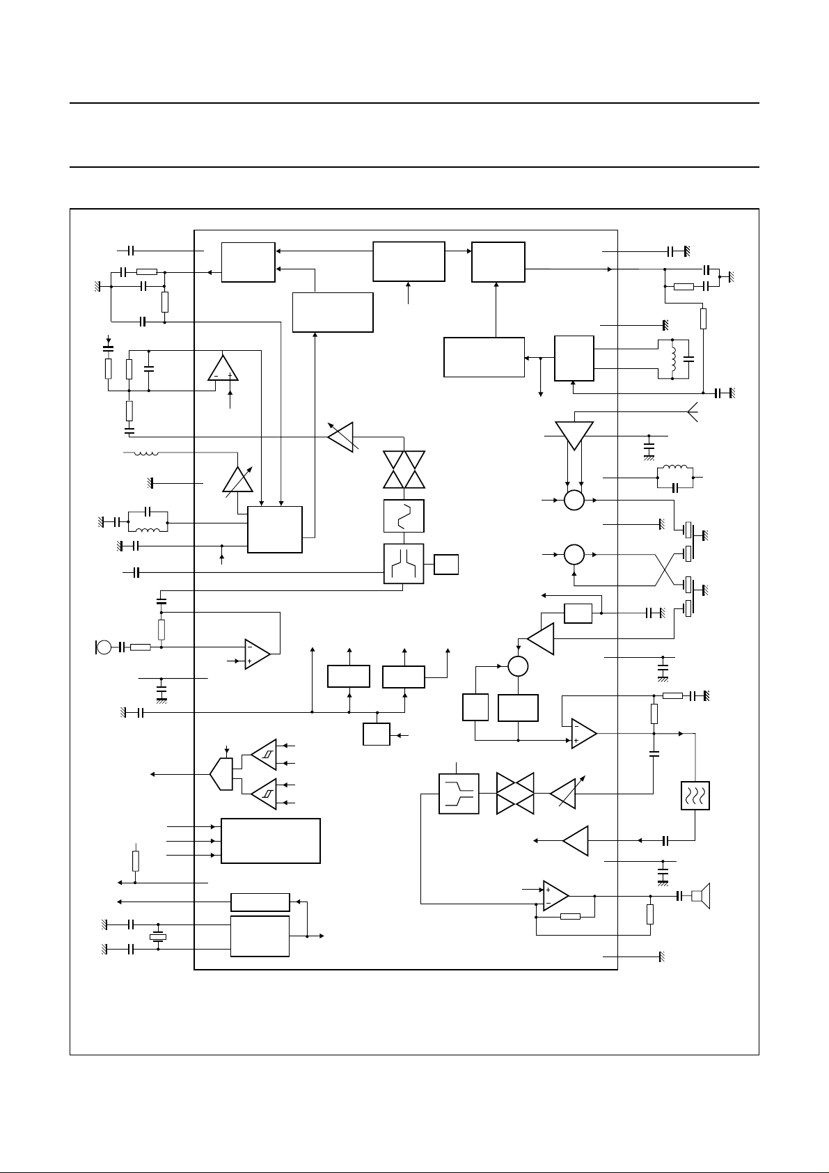
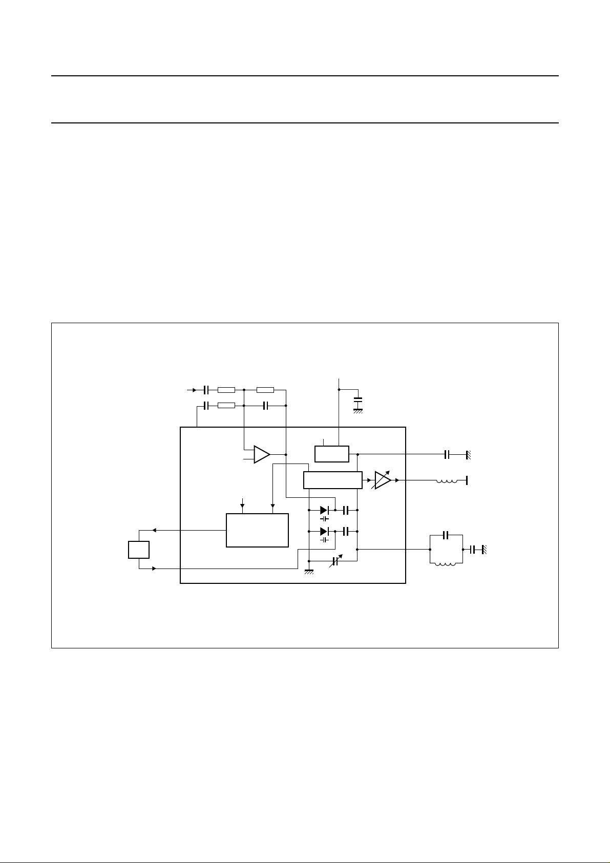
BLOCK DIAGRAM
handbook, full pagewidth
V
CC
data TX
V
CC
V
CC
V
CC(AUTX)
V
CC
220 kΩ
(1)
crystal
ECAP 1
TXPD 2
TXLF 3
MODO 4
MODI 5
TXO 6
PAO 7
TXGND
LO3I
V
REFTX
CCAP
CMPI
MICO
MICI
VB
CDBDO
EN
DATA 19
CLK
DATO
CLKO
LO2O
LO2I
TX PHASE
DETECTOR
VBMOD
PA
8
9
10
V
REFTX
11
12
13
microphone
amplifier
14
VB
15
16
CD/BD
17
18
MICROCONTROLLER
20
21
22
23
24
CRYSTAL
OSCILLATOR
TX VCO
LBD
CD
SERIAL
INTERFACE
DIVIDER
14-BIT TX
PROGRAMMABLE
DIVIDER
TX gain
CCAP
V
ref(PLL)
VB
REG 3 V
VB
V
CC
VB
RSSI
VB
LO2
REFERENCE
DIVIDER
(2048 or 892)
V
REFTX
REG 3 V
V
ref
LO2
TX mute
compressor
VB
V
CC(AU)
14-BIT RX
PROGRAMMABLE
DIVIDER
hard
limiter
ALC
UAA2062
VBMOD
VCO
ECAP
expander
RX PHASE
DETECTOR
LOOP
FILTER
RX mute
DATO
VB
×
BPFI
LO1
LO2
RSSI
LO1
LIM
data
amplifier
earpiece
amplifier
RX
VCO
LNA
1st mixer
2nd mixer
RSSI
amplifier
RX gain
V
ref(PLL)
48
47
RXPD
PLLGND
46
LO1O
45
LO1I
44
RXLF
43
RFI
42
V
CC(LNA)
41
BPFI
40
MX1O
39
×
RFGND
38
MX2O
37
×
MX2I36
RSSI
35
LIMI34
V
CC(RF)
33
PLLO32
DETO
31
RXI
30
DATI
29
V
CC(AU)
28
EARO
27
EARI
26
AUGND
25
RF
V
1st IF filter
2nd IF filter
CC
(1)
(1)
(1) Values are depending on country application (see definition in Chapter “Channel frequencies”).
Fig.1 Block diagram.
2000 Aug 10 3
FCA120
Page 4
Philips Semiconductors Product specification
Analog cordless telephone IC UAA2062
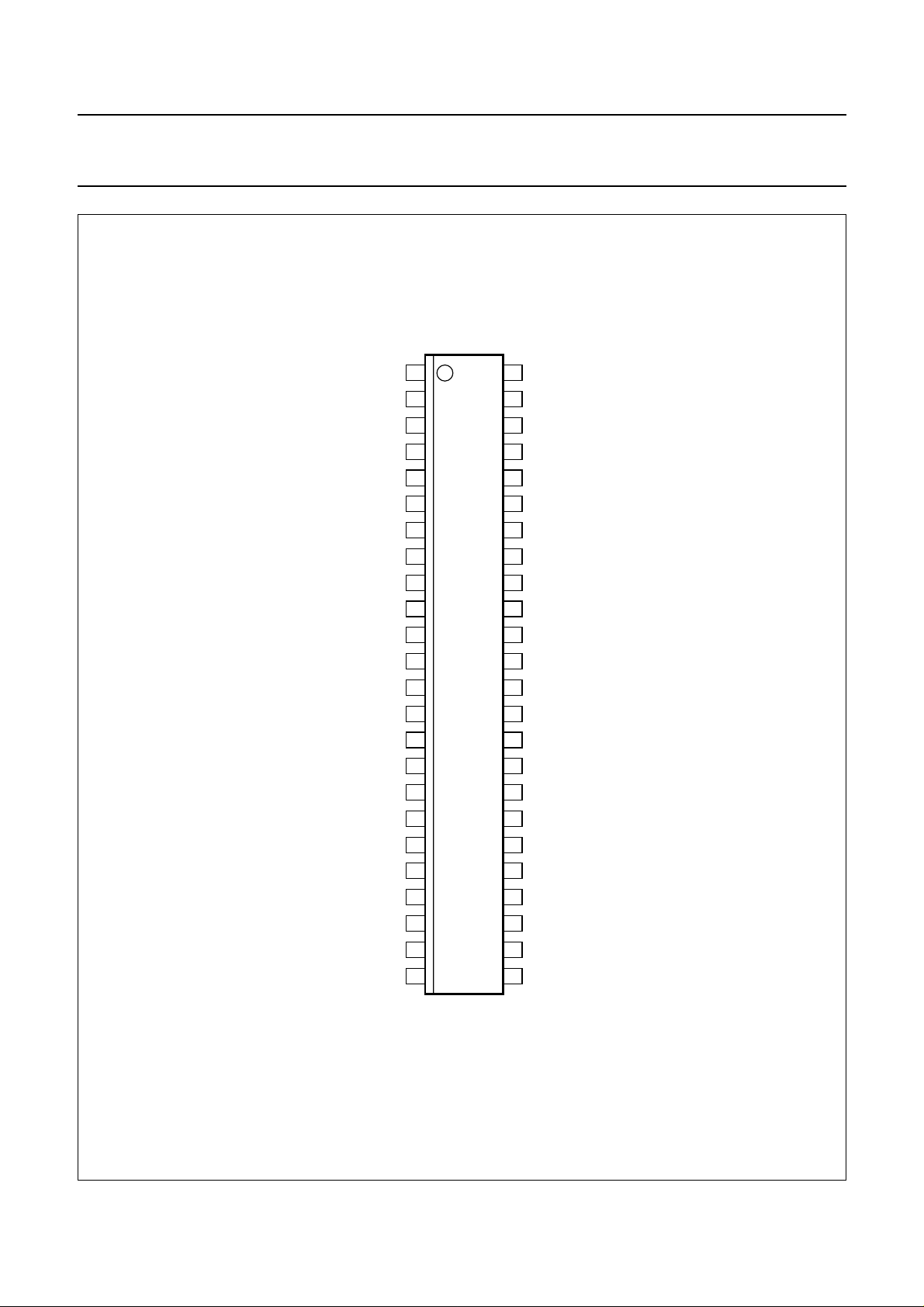
PINNING
SYMBOL PIN DESCRIPTION
ECAP 1 output pin for external capacitor
from expander
TXPD 2 phase detector output voltage for
TX PLL
TXLF 3 input from loop filter to TX VCO
MODO 4 summing amplifier output voltage
MODI 5 summing amplifier inverting input
TXO 6 TX baseband output voltage
PAO 7 power amplifier output
TXGND 8 ground for RF TX chain and PA
LO3I 9 TX VCO input
V
REFTX
10 output pin for decoupling
capacitorforregulatedvoltagefor
TX VCO
CCAP 11 output pin for external capacitor
from compressor
CMPI 12 compressor input voltage
MICO 13 microphone amplifier output
voltage
MICI 14 microphone amplifier inverting
input
V
CC(AUTX)
15 supply voltage for TX audio
VB 16 internal voltage reference
CDBDO 17 multiplexed output from carrier
detector or low-battery detector
EN 18 enable signal for serial interface
DATA 19 data signal for serial interface
CLK 20 clock signal for serial interface
DATO 21 data comparator output
CLKO 22 output pin for external clock
LO2O 23 crystal oscillator output
SYMBOL PIN DESCRIPTION
LO2I 24 crystal oscillator input
AUGND 25 ground for audio part
EARI 26 earpiece amplifier inverting input
EARO 27 earpiece amplifier output voltage
V
CC(AU)
28 supply voltage for audio part
DATI 29 data comparator input
RXI 30 RX audio input voltage
DETO 31 amplifier FM PLL output voltage
PLLO 32 amplifier FM PLL inverting input
V
CC(RF)
33 supply voltage for RF RX
LIMI 34 limiter input voltage
RSSI 35 output pin for external capacitor
from RSSI
MX2I 36 2nd mixer input
MX2O 37 2nd mixer output
RFGND 38 ground for RF RX
MX1O 39 1st mixer output voltage
BPFI 40 LNA output for external LC
V
CC(LNA)
41 supply voltage for LNA
RFI 42 LNA input voltage
RXLF 43 input from loop filter to RX VCO
LO1I 44 input pin to connect the
external LC for RX VCO
LO1O 45 output pin to connect the
external LC for RX VCO
PLLGND 46 ground for digital part of the PLL
RXPD 47 phase detector output voltage for
RX PLL
V
ref(PLL)
48 output pin for decoupling
capacitorforregulatedvoltagefor
internal PLLs and microcontroller
2000 Aug 10 4
Page 5
Philips Semiconductors Product specification
Analog cordless telephone IC UAA2062
handbook, halfpage
V
CC(AUTX)
ECAP
TXPD
TXLF
MODO
MODI
TXO
PAO
TXGND
LO3I
V
REFTX
CCAP
CMPI
MICO
MICI
CDBDO
DATA
CLK
DATO
CLKO
LO2O
LO2I
VB
EN
1
2
3
4
5
6
7
8
9
10
11
12
13
14
15
16
17
18
19
20
21
22
23
24
UAA2062
FCA091
48
47
46
45
44
43
42
41
40
39
38
37
36
35
34
33
32
31
30
29
28
27
26
25
V
ref(PLL)
RXPD
PLLGND
LO1O
LO1I
RXLF
RFI
V
CC(LNA)
BPFI
MX1O
RFGND
MX2O
MX2I
RSSI
LIMI
V
CC(RF)
PLLO
DETO
RXI
DATI
V
CC(AU)
EARO
EARI
AUGND
Fig.2 Pin configuration.
2000 Aug 10 5
Page 6
Philips Semiconductors Product specification
Analog cordless telephone IC UAA2062
FUNCTIONAL DESCRIPTION
Power supply and power management
1. In the active mode all blocks are powered.
2. In the RX mode, all circuitry in the receiver part is
powered.
POWER SUPPLY VOLTAGE
TheUAA2062is used in a cordless telephone handsetand
inabaseunit.The handset unit is battery poweredandcan
operateonthreeNiCadcells.Theminimumsupply voltage
(VCC) is 3.0 V. However the low-battery detector, crystal
oscillator, clock divider and internal voltage regulator will
function with a supply voltage of 2.85 V.
3. In the standby mode, all circuitry is powered down
except the crystal oscillator, the microcontroller
interface and the V
ref(PLL)
block.
4. In the inactive mode, all circuitry is powered down
except the microcontroller interface and the V
ref(PLL)
block.
Latch memory is maintained in all modes. Table 1 shows
POWER SAVING OPERATION MODES
which blocks are powered in each mode.
When the UAA2062is used in a handset, it is important to
reducethecurrentconsumption.There are 3 powersaving
modes in addition to the active mode:
Table 1 Power saving operation modes
CIRCUIT BLOCK
ACTIVE
MODE
RX MODE
STANDBY
MODE
INACTIVE
MODE
Microcontroller interface XXXX
V
ref(PLL)
XXX
(1)
(1)
X
Crystal oscillator X X X −
RF receiver and RX PLL X X −−
VB reference X X −−
Carrier and low-battery detectors X X −−
Data comparator X X −−
TX PLL and PA X −−−
RX and TX audio paths X −−−
Note
1. In the standby mode and in the inactive mode, by default, V
(bit V
disable is logic 0). If bit V
REFPLL
disable is logic 1, V
REFPLL
remains regulated but is not calibrated
ref(PLL)
is not regulated and fluctuates with VCC.
ref(PLL)
MAXIMUM CURRENT CONSUMPTION
Table 2 shows the typical and the maximum current consumption in the active mode and the three current saving modes
under the followingconditions:IP3HIGHmode (bit IP3 is logic 1), see Table 6; LNA gain is step 3 (bits LNA are logic 11),
see Table 12 and the PA output level is step 3 (bits PA are logic 11), see Table15.
In the standby mode and in the inactive mode, pin V
is not powered (bit V
ref(PLL)
disable is logic 1) and the clock
REFPLL
output signal is disabled (bits clock divider ratio are logic 00).
2000 Aug 10 6
Page 7

Philips Semiconductors Product specification
Analog cordless telephone IC UAA2062
Table 2 Current consumption in the 4 operating modes (VCC= 3.6 V; T
=25°C); see Table 5 for programming of
amb
the power saving operation modes
POWER OPERATING MODE
TYPICAL CURRENT
CONSUMPTION (mA)
MAXIMUM CURRENT
CONSUMPTION (mA)
active mode 27 36
RX mode 11 15
standby mode 0.35 0.5
inactive mode 0.05 0.1
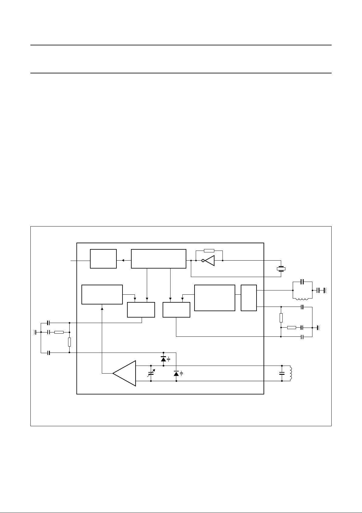
The FM receiver part
FM
RECEIVER
The FM receiver has the programmability to operate for all country channels, including the 25 U.S. channels, without the
need for external switching circuitry (see Fig.3).
The gain and input impedance of the LNA are programmable. The LNA also includes a programmable capacitance to
avoid external manual fine tuning.
handbook, full pagewidth
RF
1st IF filter
(1)
2nd IF filter
(1)
RFI
42
LNA
DUAL PLL
FREQUENCY
SYNTHESIZER
47
RXPD43RXLF45LO1O44LO1I
LPF
(1) Values depend on the country application (see definition in Chapter “Channel frequencies”).
BPFI
40
MX1O
39
MX2I
36
MX2O34LIMI
37
IF limiter
× × ×
1st mixer 2nd mixer
RSSI
RX VCO
CRYSTAL
OSCILLATOR
24
LO2I23LO2O35RSSI
crystal
(1)
Fig.3 FM receiver schematic diagram.
PLLO31DETO
32
LOOP
FILTER
VCO
V
ref
amplifier
carrier
detect output
FCA121
2000 Aug 10 7
Page 8
Philips Semiconductors Product specification
Analog cordless telephone IC UAA2062
DATA COMPARATOR
The data comparator is an inverting hysteresis
comparator. An external filter is connected between
pins DETO and DATI (AC-coupled). The open-collector
output is current limited to control the output signal slew
rate. The external resistor at pin DATO, connected to VCC,
should be 220 kΩ. An external capacitor in parallel with
this resistor will reduce the slew rate.
The transmit part
The transmitter architecture is of the direct modulation
type. The transmit VCO can be frequency modulated
either by speech or data (see Fig.4).
handbook, full pagewidth
data TX
TXO
MODI5MODO
6
VBMOD
summing
amplifier
10.24 MHz
TRANSMIT VCO
Before the VCO, an amplifier sums the modulating signal
and the data TX signal. The Colpitts type transmit VCO
includesintegratedvaricaps.Fixedexternal capacitors are
used to extend the tuning range for all countries.
The internal capacitors are programmed via the serial bus
interface. The power amplifier is capable of driving
50 Ω AC. The output level is also programmed with 2 bits
via the serial bus interface. An internal regulator supplies
the TX VCO.
V
CC(AUTX)
VB
REG 3 V
TX VCO
15
V
10
REFTX
PAO
7
PA
4
2TXPD
LPF
3TXLF
DUAL PLL
FREQUENCY
SYNTHESIZER
Fig.4 Transmit schematic diagram.
2000 Aug 10 8
9 LO3I
FCA122
Page 9
Philips Semiconductors Product specification
Analog cordless telephone IC UAA2062
The synthesizer
The synthesizer has been designed to support most
country channel frequencies between 25 and 50 MHz
(see Chapter “Channel frequencies”).
The local oscillator LO2 and the reference divider provide
the reference frequency for the RX and TX PLL loops.
A singlebitprogrammesthedividervaluefor the reference
divider. A 5 kHz reference frequency (respectively
12.5 kHz) is used with a 10.24 MHz crystal frequency
(respectively 11.15 MHz). The clock divider ratio can be
programmed to 2.5 or to 80. The ratio 80 can be chosen
whenthe IC is in sleep modetoobtaincurrentsavinginthe
microcontroller. The clock output is a CMOS output
inverter, supplied by V
ref(PLL)
.
The 14-bit TX counter is programmed for the desired
transmit channel frequency. The 14-bit RX counter is
programmed for the desired RX VCO frequency.
ndbook, full pagewidth
CLOCK
22CLKO
DIVIDER
1-BIT PROGRAMMABLE
REFERENCE COUNTER
/2048 or /892
All counters power-up in the proper default state and for a
10.24 MHz reference crystal. Both RX and TX phase
detectors have current drive type outputs of 400 µA.
The RX VCO is connected to an external capacitor and
inductor as illustrated in Fig.5. The varicaps are integrated.
Operating in the 25 US channels, there is a large
frequency difference between the minimum and the
maximum channel frequencies. The sensitivity of the
RX VCO is not large enough to accommodate this large
frequency range. Internal programmable capacitors can
be connected across the RX VCO tank circuit to change
the RX VCO sensitivity. The TX VCO also has internal
programmable capacitors to accommodate a large
frequency range. Chapter “Channel frequencies” shows
the frequency selection for all countries.
24
LO2I
crystal oscillator
23
LO2O
C1
C2
C3
R2
R3
RXLF
14-BIT
PROGRAMMABLE
RX COUNTER
47RXPD
43
PROGRAMMABLE
RX PHASE
DETECTOR
RX VCO
TX PHASE
DETECTOR
Fig.5 Synthesizer schematic diagram.
14-BIT
TX COUNTER
TX
VCO
9 LO3I
3
2 TXPD
44 LO1I
45 LO1O
FCA123
TXLF
R6
R5
C6
C5
C4
2000 Aug 10 9
Page 10
Philips Semiconductors Product specification
Analog cordless telephone IC UAA2062
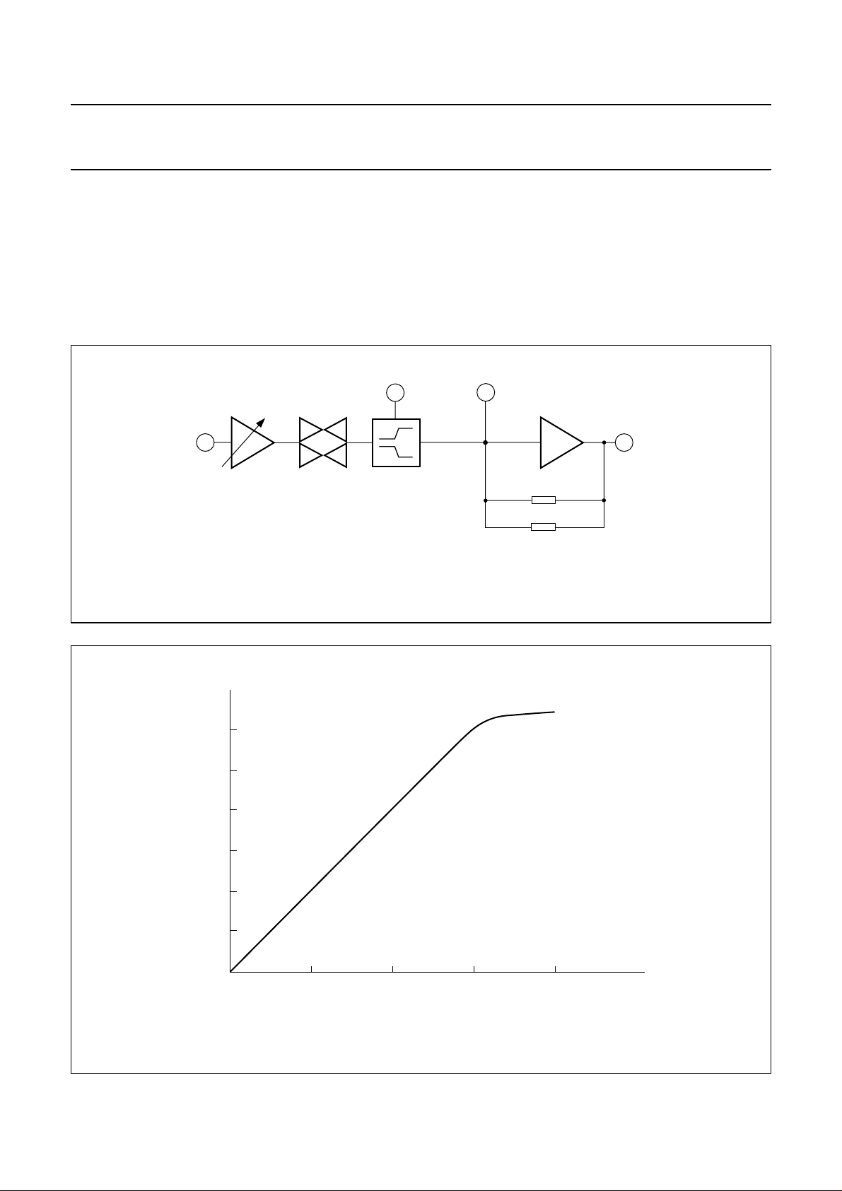
The RX baseband
This section covers the RX audio path from pins RXI to
EARO. The RXI input signal is AC-coupled.
The microcontroller sets the value of the RX gain by
32 linear steps of 0.5 dB. The RX baseband has a mute
and an expander with the characteristics shown in Fig.7.
handbook, full pagewidth
RXI
30
RX gain
RX mute
ECAP
expander
Fig.6 RX baseband schematic diagram.
EARPIECE AMPLIFIER
The earpiece amplifier is an inverting rail-to-rail
operational amplifier. The non-inverting input is connected
to the internal reference voltage VB. Internal resistors are
used to set the gain at 6 dB. An external resistor
(connected between pins EARI and EARO) can be used
to reduce the gain.
EARI
1
26
earpiece amplifier
EARO
27
internal resistor : 28 kΩ
external resistor
FCA124
handbook, full pagewidth
(1) ∆G
ARX
= 0 dB, G
EARO
(dBV)
0
−10
−20
−30
−40
−50
−60
−40 −30
= 0 dB (external resistor of 28 kΩ).
EAR
−40
−20
−20 −10 0
Fig.7 Expander characteristic.
2000 Aug 10 10
FCA127
EARO = −7 dBV typical at THD = 5%
RXI (dBV)
Page 11
Philips Semiconductors Product specification
Analog cordless telephone IC UAA2062
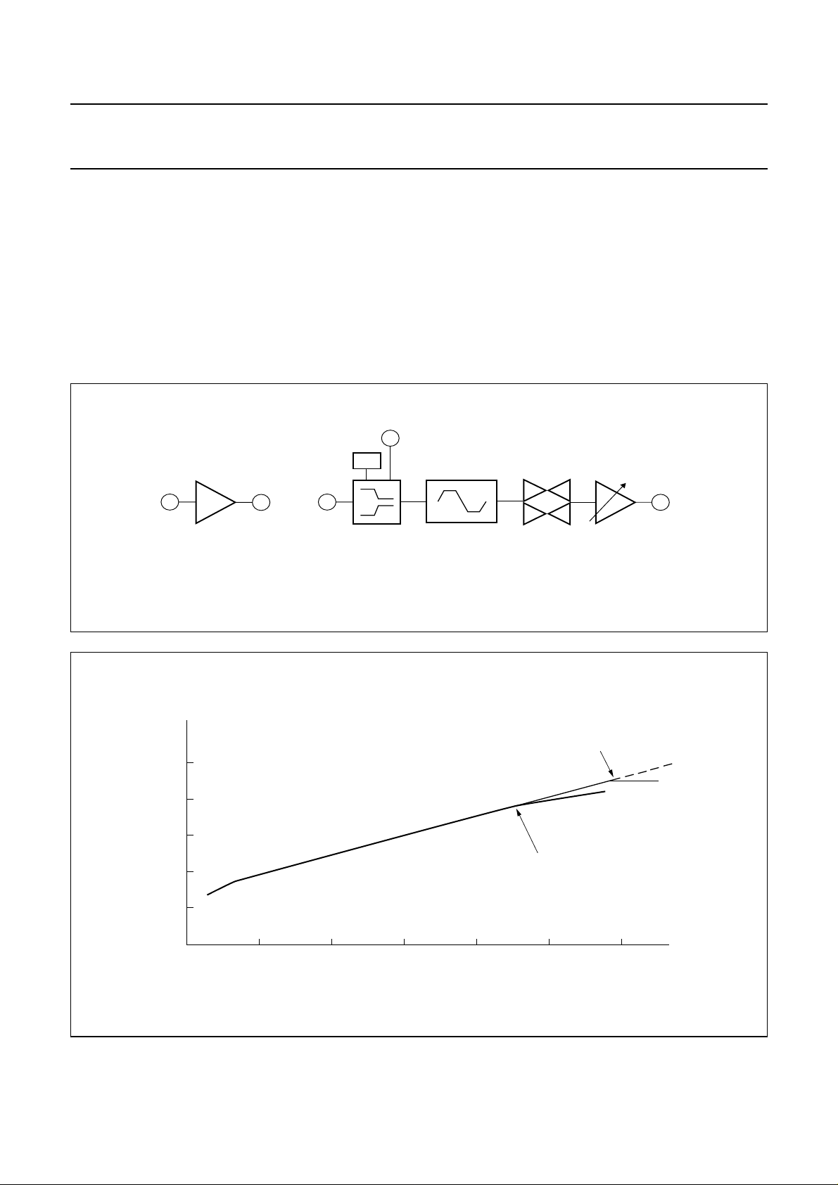
The TX baseband
This section covers the TX audio path from pins MICI to
TXO.
The microphone amplifier is an inverting operational
amplifier whose gain can be set by external resistors. The
input signal at pin MICI and the output signal at pin MOCO
arebothAC-coupled.Thenon-invertinginputisconnected
to the internal reference voltage VB. External resistors are
used to set the gain and frequency response.
handbook, full pagewidth
MICI
14
microphone
amplifier
MICO
13
CMPI
12
CCAP
11
ALC
The TX baseband has a compressor with the
characteristicshowninFig.9. The Automatic Level Control
(ALC) provides a ‘soft’ limit to the output signal swing as
the input voltage increases slowly (i.e. a sine wave is
maintained at the output). A hard limiter clamps the
compressor output voltage at 1.26 V (p-p). The ALC and
the hard limiter can be disabled via the microcontroller
interface. The hard limiter is followed by a mute circuit.
The TX gain is digitally programmable in 32 steps of
0.5 dB.
TXO
6
hard limiter
TX mutecompressor
TX gain
FCA125
handbook, full pagewidth
TXO
(dBV)
0
−10
−20
−30
−40
−60 −50
−30
Fig.8 TX baseband schematic diagram.
V
= −4 dBV; V
CMPI
(hard limiting signals)
−20
V
CMPI
−40 −30 −20 −10 0
= −1.26 V(p-p)
TXO
V
CMPI
V
= −11.5 dBV
TXO
= −16 dBV; V
(slowly changing ALC signals)
CMPI (dBV)
Fig.9 Compressor characteristic.
= −2.5 dBV
TXO
= −13 dBV
FCA126
2000 Aug 10 11
Page 12
Philips Semiconductors Product specification
Analog cordless telephone IC UAA2062
Other features
PLL VOLTAGE REGULATOR
Pin V
RX and TX PLLs. It is regulated at 3 V. Pin V
provides the internal supply voltage for the
ref(PLL)
CC(AU)
provides the supply voltage input for the internal voltage
regulator. Two capacitors of 47 µF and 100 nF must be
connected to pin V
to filter and stabilize this
ref(PLL)
regulated voltage. The tolerance of the regulated voltage
is initially ±8% but is improved to ±4% after the internal
band gap voltage reference is adjusted via the
microcontroller.
The voltage regulator is always turned on. In the inactive
mode the calibration is turned off to reduce current
consumption. In this mode, the V
block supplies
ref(PLL)
300 µA to the microcontroller. The output drive capability
is 3 mA. The voltage regulator is able to supply the
microcontroller.
The local oscillator LO2 and the RX and TX phase
detectors are powered by the internal voltage regulator at
pin V
. Therefore, the maximum input and output
ref(PLL)
level for most I/O pins (LO2I and LO2O) equals the
regulated voltage at pin V
ref(PLL)
.
The comparator has a built-in hysteresis to prevent
spuriousswitching.Theprecision of thedetectiondepends
on the divider accuracy, the comparator offset and the
accuracy of the reference voltage VB. The output is
multiplexed at pin CDBDO. When the battery voltage level
is below the threshold voltage the output CDBDO is going
LOW.
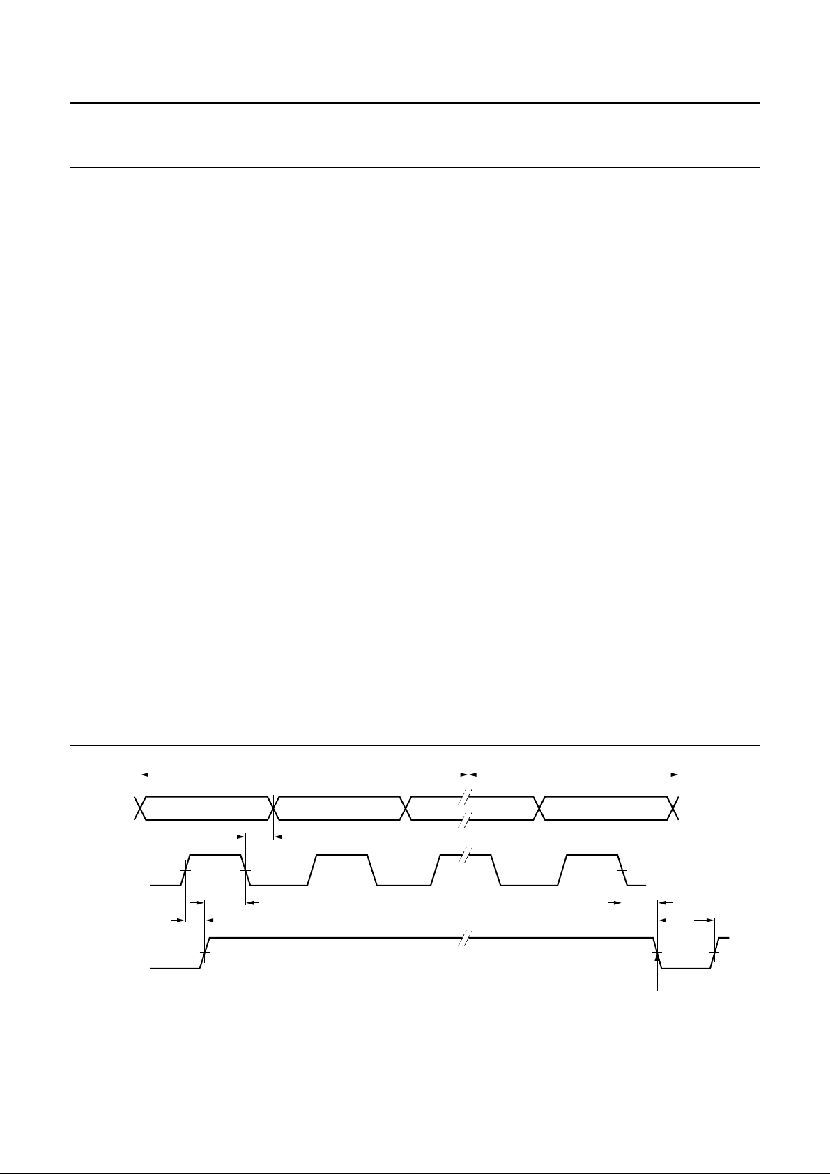
Microcontroller serial interface
Pins DATA, CLK and EN provide a 3-wire unidirectional
serial interface for programming the reference counters,
the transmit and receive channel divider counters and the
control functions.
Theinterfaceconsists of 18-bit shift registers connected to
a matrix of registers organized as 6 words of 18 bits. The
leading 15 bits include the data D14 to D0. The trailing
3 bits set up the address AD2 to AD0. The data is entered
with the most significant bit D14 first. The last bit is
bit AD0.
Pins DATA and CLK are used to load data into the shift
register. Figure 10 shows the timing required on all pins.
Data is clocked into the shift registers on negative clock
transitions.
LOW-BATTERY DETECTOR
The low-battery detector measures the voltage level of the
V
using a resistance divider and a comparator. One
CC(AU)
inputofthecomparatoris connected to VB,theothertothe
middle point of the resistance divider.
handbook, full pagewidth
DATA
CLK
EN
D14 D13 D12 AD1 AD0
50%
t
HD;EC
t
SU;CE
50%
data bits (15) address bits (3)
t
SU;DC
50%
The serial interface pins DATA, CLK and EN, are supplied
by V
. Internal level shifters are provided after the
ref(PLL)
pins which allow the logic and registers to be internally
powered by V
CC(AU)
.
TheESD protection diodes on these pins are connected to
V
. All the digital outputs (CDBDO and DATO) are
CC(AU)
open-collector outputs.
t
END
t
w
data bits latched
MGR004
Fig.10 Digital signals timing requirement.
2000 Aug 10 12
Page 13

Philips Semiconductors Product specification
Analog cordless telephone IC UAA2062
DATA REGISTERS AND ADDRESSES
Table 3 shows the data latches and addresses which are used to select each of the registers. bit D14 is the MSB and is
written and loaded first.
Table 3 Data register and addresses
ADDR D14 D13 D12 D11 D10 D9 D8 D7 D6 D5 D4 D3 D2 D1 D0
001 − TX counter [13 to 0]
010 − RX counter [13 to 0]
011 voltage reference
adjust [2 to 0]
100 test modes [2 to 0]
101 BD
active
low-battery
detector threshold
[2 to 0]
110 activemodes
PA [1 and 0] TX VCO capacitor
[1 and 0]
Clk Div
[1 and 0]
(1)
LNA capacitor [3 to 0] RX VCO capacitor [3 to 0] FM PLL centre frequency
Ref
IP3 LNA gain
Div
[1 and 0]
LNA RIN
[1 and 0]
CD threshold control [4 to 0] RX
V
REFPLL
disable
RX gain control[4 to 0]
mute
selection[3 to 0]
ALC
disableTXmute
TX gain control[4 to 0]
HLim −
shift [3 to 0]
Note
1. The three bits must be set at 000 in normal operation.
Table 4 Data register default value
ADDR D14 D13 D12 D11 D10 D9 D8 D7 D6 D5 D4 D3 D2 D1 D0
001 − 10011011101110
010 − 01110000101111
0110110100000001−−
100000000000000111
101000000000001111
110001101110001111
ACTIVE MODES BITS SELECTION
Table 5 Active modes bits selection
BIT 1 BIT 0 DESCRIPTION
0 0 active mode
0 1 RX mode
1 0 standby mode
1 1 inactive mode
2000 Aug 10 13
Page 14

Philips Semiconductors Product specification
Analog cordless telephone IC UAA2062
REGISTER CONTENT DESCRIPTION
Table 6 Register content description
DATA REGISTER BIT DESCRIPTION
IP3 1 IP3 HIGH mode for 2nd mixer
0 IP3 LOW mode for 2nd mixer
ALC disable 1 automatic level control disabled
0 normal operation
HLim 1 hard limiter disabled
0 normal operation
RX mute 1 RX channel muted
0 normal operation
TX mute 1 TX channel muted
0 normal operation
LBD enable 1 low-battery detector enabled
0 carrier detector enabled
V
Ref Div 1 divider ratio 892 (conversion from 11.15 MHz to 12.5 kHz)
disable 1 V
REFPLL
disabled (tied to VCC)
REFPLL
0V
REFPLL
enabled
0 divider ratio 2048 (conversion from 10.24 MHz to 5 kHz)
2000 Aug 10 14
Page 15

Philips Semiconductors Product specification
Analog cordless telephone IC UAA2062
TX AND RX GAIN SELECTION
The TX and RX audio signal paths have a programmable gain block. If a TX or RX voltage gain other than the nominal
power-up default is desired it can be programmed via the microcontroller interface.
The gain blocks can be used during final test of the telephone to electronically adjust for gain tolerances in the telephone
system. The RX gain and the TX gain selection covers a dynamic range from −7.5 to +8 dB in steps of 0.5 dB and can
be programmed independently from each other.
Table 7 TX and RX gain selection
BIT 4 BIT 3 BIT 2 BIT 1 BIT 0 STEP
000000−7.5 −7.5
000011−7.0 −7.0
000102−6.5 −6.5
000113−6.0 −6.0
001004−5.5 −5.5
001015−5.0 −5.0
001106−4.5 −4.5
001117−4.0 −4.0
010008−3.5 −3.5
010019−3.0 −3.0
0101010−2.5 −2.5
0101111−2.0 −2.0
0110012−1.5 −1.5
0110113−1.0 −1.0
0111014−0.5 −0.5
011111500
1 0 0 0 0 16 +0.5 +0.5
1 0 0 0 1 17 +1.0 +1.0
1 0 0 1 0 18 +1.5 +1.5
1 0 0 1 1 19 +2.0 +2.0
1 0 1 0 0 20 +2.5 +2.5
1 0 1 0 1 21 +3.0 +3.0
1 0 1 1 0 22 +3.5 +3.5
1 0 1 1 1 23 +4.0 +4.0
1 1 0 0 0 24 +4.5 +4.5
1 1 0 0 1 25 +5.0 +5.0
1 1 0 1 0 26 +5.5 +5.5
1 1 0 1 1 27 +6.0 +6.0
1 1 1 0 0 28 +6.5 +6.5
1 1 1 0 1 29 +7.0 +7.0
1 1 1 1 0 30 +7.5 +7.5
1 1 1 1 1 31 +8.0 +8.0
TX GAIN
(dB)
RX GAIN
(dB)
2000 Aug 10 15
Page 16

Philips Semiconductors Product specification
Analog cordless telephone IC UAA2062
CARRIER DETECTOR THRESHOLD SELECTION
The carrier detector indicates if a carrier signal is present on the selected channel. The nominal value and tolerance of
the carrier detector threshold is given in the carrier detector specification section. If a different carrier detector threshold
value is desired, it can be selected via the microcontroller interface.
If it is required to scale the carrier detector range, an external resistor should be connected between pin RSSI and
ground. The carrier detector threshold step 19 (10011) corresponds to a typical level on pin RSSI of 0.86 V DC.
Table 8 Carrier detector threshold selection
BIT 4 BIT 3 BIT 2 BIT 1 BIT 0 STEP
00000 0 0.1
00001 1 0.14
00010 2 0.18
00011 3 0.22
00100 4 0.26
00101 5 0.3
00110 6 0.34
00111 7 0.38
01000 8 0.42
01001 9 0.46
01010 10 0.5
01011 11 0.54
01100 12 0.58
01101 13 0.62
01110 14 0.66
01111 15 0.7
10000 16 0.74
10001 17 0.78
10010 18 0.82
10011 19 0.86
10100 20 0.9
10101 21 0.94
10110 22 0.98
10111 23 1.02
11000 24 1.06
11001 25 1.1
11010 26 1.14
11011 27 1.18
11100 28 1.22
11101 29 1.26
11110 30 1.3
11111 31 1.34
CARRIER DETECTOR
THRESHOLD (V)
2000 Aug 10 16
Page 17

Philips Semiconductors Product specification
Analog cordless telephone IC UAA2062
LOW-BATTERY DETECTOR LEVEL SELECTION
When the LBD register is set HIGH, the low-battery detector is enabled and the low-battery detect output signal is routed
to the output pin CDBDO.Thelow-battery detector levelselectionfunctions only in a programmablemode.Thepower-up
default value is step 7 (111).
Table 9 Low-battery detector level selection
NOMINAL
BIT 2 BIT 1 BIT 0 STEP
00003.6
00113.5
01023.4
01133.3
10043.2
10153.1
11063.0
11172.9
LOW-BATTERY
DETECTOR
VOLTAGE (V)
VOLTAGE REFERENCE SELECTION
An internal 1.5 V band gap reference voltage provides the voltage reference for the low-battery detector circuit, the
V
Table 10 Voltage reference selection
voltage regulator, the VB reference and all internal analog references.
ref(PLL)
BIT 2 BIT 1 BIT 0 STEP
0000−7
0011−5
0102−3
0113−1
1004+1
1015+3
1106+5
1117+7
NOMINAL VOLTAGE
REFERENCE (%)
2000 Aug 10 17
Page 18

Philips Semiconductors Product specification
Analog cordless telephone IC UAA2062
LNA CAPACITOR SELECTION
The LNA has an external capacitor and inductor that together form a band-pass filter. A programmable on-chip capacitor
is integrated which gives, in parallel with an external L and C, the possibility to tune the band-pass filter characteristic
during production. A parasitic capacitor has to be added to the internal capacitor value.
Table 11 LNA capacitor selection
BIT 3 BIT 2 BIT 1 BIT 0 STEP
00000 0
00011 0.8
00102 1.6
00113 2.4
01004 3.2
01015 4.0
01106 4.8
01117 5.6
10008 6.4
10019 7.2
101010 8.0
101111 8.8
110012 9.6
110113 10.4
111014 11.2
111115 12.0
LNACAPACITORVALUE
(pF)
2000 Aug 10 18
Page 19

Philips Semiconductors Product specification
Analog cordless telephone IC UAA2062
LNA GAIN SELECTION
The LNA has an internal programmable voltage conversiongain. This allows to tune the gain in order to achieve the best
compromise in term of performance. The LNA gain is given with a reference value of L = 390 nH (Q
50 MHz.
loaded
= 40) at
Table 12 LNA gain selection; L = 390 nH at BPFI; Q
= 40; f = 50 MHz
Loaded
BIT 1 BIT 0 STEP LNA GAIN (dB)
00017
01119
10221
11323
INPUT RESISTIVE IMPEDANCE SELECTION
LNA
The LNA has an internal programmable input resistive impedance (RIN) in order to improve the duplexer and LNA
performance. To calculate the input resistive impedance we must know the typical LNA gain (i.e. the value of the external
inductance and its Q). A small capacitance at the LNA input is needed to improve matching between LNA and duplexer.
The programmability of tuning the input impedance allows to obtain an optimum sensitivity performance in the active and
in the RX mode of operation.
Table 13 LNA input resistive impedance selection
TYPICAL LNA INPUT RESISTIVE IMPEDANCE
BIT 1 BIT 0 STEP
LNA VOLTAGE
GAIN = 17 dB
LNA VOLTAGE
GAIN = 23 dB
0 0 0 1.2 kΩ 645 Ω
0 1 1 3.0 kΩ 1.6 kΩ
1 0 2 7.1 kΩ 3.8 kΩ
1 1 3 22.9 kΩ 14.5 kΩ
2000 Aug 10 19
Page 20

Philips Semiconductors Product specification
Analog cordless telephone IC UAA2062
RX AND TX VCO CAPACITOR SELECTION
The RX VCO and the TX VCO have an external LC tank circuit. A programmable internal capacitor is integrated in
parallel with the external L and C in order to tune the VCO and to keep the PLL in lock for large frequency steps.
A parasitic capacitor has to be added to these values. The RX VCO capacitor value and the TX VCO capacitor value can
be programmed independently one from the other.
Table 14 RX and TX VCO capacitor selection
INTERNAL
BIT 3 BIT 2 BIT 1 BIT 0 STEP
0000000
000110.90.45
001021.80.9
001132.71.35
010043.61.8
010154.52.25
011065.42.7
011176.33.15
100087.23.6
100198.14.05
1010109.04.5
1011119.94.95
11001210.8 5.4
11011311.7 5.85
11101412.6 6.3
11111513.5 6.75
RX VCO
CAPACITOR
VALUE (pF)
INTERNAL
TX VCO
CAPACITOR
VALUE (pF)
PA OUTPUT LEVEL SELECTION
The power amplifier has 2 bits to select the output voltage level. The power-up default value is step 3 (11). VCC= 3.6 V.
Table 15 PA output level selection
BIT 1 BIT 0 STEP PA OUTPUT POWER (dB)
000−4
011−2
1020
113+2
2000 Aug 10 20
Page 21

Philips Semiconductors Product specification
Analog cordless telephone IC UAA2062
FM PLL CENTRE FREQUENCY SHIFT SELECTION
This programming enables to shift the centre frequency of the VCO, within the FM PLL, in order to align the frequency
as close as possible to the 2nd IF frequency (nominal frequency 455 kHz).
Table 16 FM PLL centre frequency shift selection
CENTRE
BIT 3 BIT 2 BIT 1 BIT 0 STEP
00000−154
00011−132
00102−110
00113−88
01004−66
01015−44
01106−22
011170
10008+22
10019+44
101010+66
101111+88
110012+110
110113+132
111014+154
111115+176
FREQUENCY
SHIFT (kHz)
CLOCK DIVIDER RATIO SELECTION
The clock output signal CLKO is derived from the local oscillator LO2 and can be used to drive a microcontroller. The
LO2 signal is divided with a programmable divider value. The divider is followed by a filter that controls the slew rate of
the signal in order to avoidradiationnoise on the PCB. The CLKO output also has the option to disable the output signal.
The default value is step 1 (01).
Table 17 Clock divider ratio selection
BIT 1 BIT 0 STEP CLOCK DIVIDER RATIO
0 0 0 output disabled
0112.5
10280
2000 Aug 10 21
Page 22

Philips Semiconductors Product specification
Analog cordless telephone IC UAA2062
LIMITING VALUES
In accordance with the Absolute Maximum Rating System (IEC 60134).
SYMBOL PARAMETER MIN. MAX. UNIT
V
CC
T
stg
T
amb
HANDLING
Inputs and outputs are protected against electrostatic discharge in normal handling. However, to be totally safe, it is
desirable to take normal precautions appropriate to handling MOS devices.
THERMAL CHARACTERISTICS
SYMBOL PARAMETER CONDITIONS VALUE UNIT
R
th(j-a)
supply voltage −0.3 +6.0 V
storage temperature −55 +125 °C
ambient temperature −10 +70 °C
thermal resistance from junction to ambient in free air 100 K/W
CHARACTERISTICS
V
CC
= 3.6 V; T
=25°C; specified for US handset applications; unless otherwise specified.
amb
SYMBOL PARAMETER CONDITIONS MIN. TYP. MAX. UNIT
Supply
V
CC
T
amb
supply voltage 3 3.6 5.25 V
ambient temperature −10 − +70 °C
FM receiver part
GENERAL FM RECEIVER SYSTEM CHARACTERISTICS; note 1
S
RFI
sensitivity at duplexer input
(50 Ω)
matched duplexer
(3 dB loss)
for 20 dB SINAD −−112 − dBm
for 12 dB SINAD
−−117 − dBm
RX mode
for 12 dB SINAD
−−116 − dBm
active mode
THD
FM
V
DETO(rms)
total harmonic distortion without CCITT filter − 2.0 3.0 %
AC output level at pin DETO
V
= −65 dBm − 100 − mV
i(RFI)
(RMS value)
S/N
FM
signal-to-noise ratio V
= −65 dBm − 45 − dB
i(RFI)
2000 Aug 10 22
Page 23

Philips Semiconductors Product specification
Analog cordless telephone IC UAA2062
SYMBOL PARAMETER CONDITIONS MIN. TYP. MAX. UNIT
LOW-NOISE AMPLIFIER; note 2
G
∆G
v(LNA)
v(LNA)
voltage conversion gain from pin RFI to
voltage conversion gain
adjustment range
N
steps(LNA)
voltage conversion gain
adjust steps
V
i(LNA)
CP1
LNA(rms)
input voltage −125 −−10 dBm
1 dB compression point
(RMS value)
F
LNA
noise figure from pin RFI to
1ST MIXER; note 3
Z
o(MX1)
G
cp(MX1)
IP3
MX1(rms)
output impedance referenced to pin BPFI − 330 −Ω
voltage conversion gain ZL= 330 Ω;
3rd-order intercept point
(RMS value)
CP1
MX1(rms)
1 dB compression point
(RMS value)
F
MX1
input referenced noise referenced to pin BPFI − 12 − nV/√Hz
2ND MIXER; note 4
Z
i(MX2)
Z
o(MX2)
G
cp(MX2)
NF
MX2
input impedance − 1.5 − kΩ
output impedance − 1.5 − kΩ
voltage conversion gain measured at
noise figure from pin MX2I
to pin MX2O
IP3
MX2(rms)
3rd order intercept
(RMS value)
pin BPFI; LNA gain
step 2; LNA RIN
step 3
from pin RFI to
pin BPFI
from pin RFI to
pin BPFI
referenced to pin RFI − 35 − mV
pin BPFI; LNA gain
step 2; LNA RIN
step 3
referenced to pin BPFI
referenced to pin BPFI − 260 − mV
referenced to pin BPFI − 100 − mV
pin MX2O
IP3 HIGH − 15 − dB
IP3 LOW − 18 − dB
measured at
pin MX2O; referenced
to pin MX2I
IP3 HIGH − 210 − mV
IP3 LOW − 150 − mV
− 21 − dB
− 6 − dB
− 4 −
− 3 − dB
− 11.5 − dB
− 15 18 dB
2000 Aug 10 23
Page 24

Philips Semiconductors Product specification
Analog cordless telephone IC UAA2062
SYMBOL PARAMETER CONDITIONS MIN. TYP. MAX. UNIT
CP1
MX2(rms)
LIMITER
Z
i(LIM)
G
v(LIM)
PLL DEMODULATOR; note 5
/∆V VCO gain after calibration − 50 − kHz/V
∆f
VCO
f
VCO
N
step(VCO)
f
VCO(st)
R
L(PLL)
V
o(PLL)(rms)
RSSI CARRIER DETECTOR; note 6
RSSI output current dynamic
V
OH
V
OL
R
i
V
det
V
det(st)
V
hys
N
step(CD)
DATA COMPARATOR
V
ac(DATI)(p-p)
V
th(DATI)
1 dB compression point
(RMS value)
measured at
pin MX2O; referenced
to pin MX2I
IP3 HIGH − 70 − mV
IP3 LOW − 50 − mV
input impedance f0= 455 kHz − 1.5 − kΩ
voltage gain f0= 455 kHz;
V
= 100 µV (RMS)
i(LIM)
VCO centre frequency free running; open
− 85 − dB
200 455 650 kHz
loop
number of steps for VCO
− 16 −
frequency adjustment
VCO centre frequency step − 22 − kHz
demodulator external load
5 −−kΩ
on pin DETO
output voltage on pin DETO
R
L(PLL)
=5kΩ− −0.4 V
(RMS value)
− 65 − dB
range
HIGH-leveloutput voltage at
pin CDBDO
LOW-level output voltage at
pin CDBDO
internal resistance between pins RSSI
CD step 19;
V
= 0.1 V (RMS)
i(LIM)
V
= 0 V (RMS);
i(LIM)
CD step 19
and V
CC(RF)
0.9V
CC
−−0.1V
−−V
V
CC
− 170 − kΩ
voltage detection 0.05 − 1.3 V
voltage detection step − 40 − mV
hysteresis voltage − 60 − mV
number of steps for carrier
sense threshold
AC input voltage
programmablethrough
microcontroller
− 32 −
75 −−mV
(peak-to-peak value)
threshold voltage on
− VCC− 0.9 − V
pin DATI
2000 Aug 10 24
Page 25

Philips Semiconductors Product specification
Analog cordless telephone IC UAA2062
SYMBOL PARAMETER CONDITIONS MIN. TYP. MAX. UNIT
Z
i(DATI)
V
OH(DATO)
V
OL(DATO)
I
o(sink)
The transmit part; note 7
General
THD
TX
Summing amplifier
V
o(SUM)
R
f(SUM)
V
bias(SUM)
Voltage controlled oscillator and power amplifier;
V
PA
N
step(PA)
V
o(PA)
H2
PA
H3
PA
f∆
(MODO)
------V∆
f∆
(TXLF)
------V∆
Q
L(VCO)
N
VCO(TX)
The synthesizer
input impedance at pin DATI − 240 − kΩ
HIGH-level output voltage
V
i(DATI)=VCC
− 1.4 V 0.9V
CC
−−V
on pin DATO
LOW-leveloutput voltage on
V
i(DATI)=VCC
− 0.4 V −−0.1V
CC
V
pin DATO
output sink current V
total harmonic distortion
after demodulation
summing amplifier output
i(DATI)=VCC
V
o(DATO)
V
= 1 mV (RMS);
MICI
CCITT filter (P53)
= 0.1V
− 0.4 V;
CC
− 20 −µA
− 2 − %
−−10 − dBV
voltage on pin MODO
summing amplifier external
feedback resistor
between pins MODI
and MODO
10 −−kΩ
DC voltage at pin MODI − 2.4 − V
note 8
PA output voltage fo= 49.97 MHz;
− 2 − dBm
PA step 3
number of steps of VCO
− 4 −
output voltage
PA output voltage −4 − +2 dB
attenuation 2nd harmonic 14 18 − dB
attenuation 3rd harmonic 26 34 − dB
VCO modulation gain V
VCO gain V
V
= 2.4 V − 15.5 − kHz/V
MODO
= 0.9 V − 550 − kHz/V
TXLF
= 1.2 V − 380 − kHz/V
TXLF
Q factor of external L filter L = 330 nH 40 −−
TX VCO phase noise f
=25to50MHz
carrier
f
= 5 kHz −−96 −80 dBc/Hz
offset
= 12.5 kHz −−104 −87 dBc/Hz
f
offset
PLL LOOP FILTER; note 9
f
C
xtal
i(LO2)
LO frequency −−12 MHz
parasitic capacitance
between pins LO2I
and LO2O
C
L(LO2)
load capacitance between
pins LO2I and LO2O
2000 Aug 10 25
−−3pF
− 15 30 pF
Page 26

Philips Semiconductors Product specification
Analog cordless telephone IC UAA2062
SYMBOL PARAMETER CONDITIONS MIN. TYP. MAX. UNIT
f
RX
N
VCO(RX)
t
strt(RXPLL)
t
res(RXPLL)
t
strt(TXPLL)
t
res(TXPLL)
f
TX
C
o(RXPD)
C
o(TXPD)
The RX baseband
RX VCO frequency 25 − 55 MHz
RX VCO phase noise at
pin LO2O
RX PLL start time measuredbyswitching
f
=25to37MHz
carrier
f
= 5 kHz −−96 −90 dBc/Hz
offset
f
= 12.5 kHz −−104 −98 dBc/Hz
offset
− 10 − ms
from inactive to active
mode
RX PLL step response time from channel 8 to
− 12 − ms
channel 10; measured
within ±500 Hz from
final frequency
TX PLL start time measuredbyswitching
− 60 − ms
from inactive to active
mode
TX PLL step response time from CH 7 to CH 10;
− 40 − ms
measured within
±500 Hz from final
frequency
TX VCO frequency 20 − 55 MHz
output capacitance at
−−8pF
pin RXPD
output capacitance at
−−8pF
pin TXPD
RX AUDIO PATH; note 10
∆G
ARX
N
step(ARX)
∆G
v(m)
G
EXP
Z
i(RXI)
t
att(EXP)
t
rel(EXP)
α
ct(EARO)
RX gain adjustment programmablethrough
RX gain adjust steps programmablethrough
RX mute V
expander gain level V
input impedance − 15 − kΩ
expander attack time C
expander release time C
compressor to expander
crosstalk attenuation
−7.5 − +8 dB
microcontroller
− 32 −
microcontroller
= −20 dBV −−70 −60 dB
i(RXI)
= −20 dBV −4 0 +4 dB
i(RXI)
= −30 dBV −14 −10 −6dB
V
i(RXI)
V
= −40 dBV −−20 − dB
i(RXI)
= 0.47 µF − 3.0 − ms
ECAP
= 0.47 µF − 13.5 − ms
ECAP
from pin CMPI to
− 70 − dB
pin EARO;
V
= 0 V (RMS);
RXI
V
= −20 dBV
CMPI
2000 Aug 10 26
Page 27

Philips Semiconductors Product specification
Analog cordless telephone IC UAA2062
SYMBOL PARAMETER CONDITIONS MIN. TYP. MAX. UNIT
EARPIECE AMPLIFIER; note 11
V
o(EARO)(p-p)
output swing voltage
(peak-to-peak value)
G
ear
R
L(EARO)
THD
N
ARX
ARX
gain earpiece amplifier no external resistor − 6 − dB
earpiece resistance note 12 − 150 −Ω
total harmonic distortion V
audio path noise B = 400 Hz to 3 kHz −−83 − dBV
The TX baseband
MICROPHONE AMPLIFIER; note 13
V
o(MICO)
∆G
V
THD
MICO
output swing RL=10kΩ− −27 −12 dBV
voltage gain adjustment 0 − 34 dB
total harmonic distortion f = 1 kHz;
TX AUDIO PATH; note 14
G
COMP
G
COMP(max)
V
HLIM(p-p)
compressor gain ALC disabled
maximum compressor gain V
output voltage hard limiter
(peak-to-peak value)
V
i(CMPI)
V
o(TXO)
THD
COMP
Z
i(CMPI)
t
att(COMP)
t
rel(COMP)
α
ct(COMP)
input voltage range −−26 −12 dBV
output voltage ALC normal operation
total harmonic distortion ALC disabled;
input impedance − 15 − kΩ
compressor attack time C
compressor release time C
expander to compressor
crosstalk attenuation
∆G
v(m)
∆G
ATX
N
step(ATX)
TX mute ALC disabled;
TX gain adjustment programmablethrough
TX gain adjustment steps programmablethrough
THD < 4% − 2.2 − V
= −20 dBV − 0.5 1 %
i(RXI)
− 0.2 − %
V
HLim disabled;
= −12 dBV
o(MICO)
V
V
V
i(CMPI)
= −10 dBV −4 0 +4 dB
i(CMPI)
= −30 dBV 6 10 14 dB
i(CMPI)
= −50 dBV 16 20 24 dB
i(CMPI)
= −70 dBV − 23 − dB
− 1.26 − V
ALC disabled;
V
i(CMPI)
V
i(CMPI)
V
i(CMPI)
V
i(CMPI)
= −4 dBV
= −12 dBV −−12.5 − dBV
= −10 dBV −−12.3 − dBV
= −2.5 dBV −−11.5 − dBV
− 0.5 1 %
V
V
= −10 dBV
i(CMPI)
= 0.47 µF − 3.0 − ms
CCAP
= 0.47 µF − 13.5 − ms
CCAP
i(CMPI)
= 0 V (RMS);
− 40 − dB
from RXI to TXO;
V
= −10 dBV
i(RXI)
−−70 −60 dB
V
i(CMPI)
= −10 dBV
−7.5 − +8 dB
microcontroller
− 32 −
microcontroller
2000 Aug 10 27
Page 28

Philips Semiconductors Product specification
Analog cordless telephone IC UAA2062
SYMBOL PARAMETER CONDITIONS MIN. TYP. MAX. UNIT
Z
o(TXO)
Other features
PLL VOLTAGE REGULATOR
V
ref(PLL)
∆V
ref(PLL)
I
o
LOW-BATTERY DETECTOR: LBD ENABLED
∆VCC/V
Characteristics of digital pins
output impedance at
− 500 −Ω
pin TXO
regulated output level before VB adjustment 2.75 3 3.25 V
after VB adjustment 2.95 3 3.05 V
load regulation VCC= 3.6 V;
− 100 − mV
Io=0to3mA
output current VCC= 3.6 V −−3mA
battery detection accuracy after VB adjustment;
CC
−3 − +3 %
low-battery detect
level step 0
MICROCONTROLLER
V
IL
LOW-level input voltage at
pins DATA, CLK and EN
V
IH
HIGH-level input voltage at
pins DATA, CLK and EN
I
IL
LOW-level input current at
pins DATA, CLK and EN
I
IH
HIGH-level input current at
pins DATA, CLK and EN
C
i
input capacitance at
pins DATA, CLK and EN
CDBDO OUTPUT
I
OL
LOW-level output current at
pin CDBDO
I
OH
HIGH-level output current at
pin CDBDO
V
OL
LOW-level output voltage at
pin CDBDO
V
OH
HIGH-leveloutput voltage at
pin CDBDO
TIMING (see Fig.10)
t
SU;CE
t
SU;DC
t
HD;EC
f
clk
t
r
t
f
set-up time CLK to EN 50% of signals 200 −−ns
set-up time DATA to CLK 50% of signals 200 −−ns
hold time EN to CLK 50% of signals 200 −−ns
clock frequency −−300 kHz
input rise time 10% to 90% −−10 ns
input fall time 10% to 90% −−10 ns
−−0.5 V
V
− 0.5 − V
ref(PLL)
CC(AU)
V
VIL= 0.3 V −5 −−µA
VIH=V
− 0.3 V −−5µA
ref(PLL)
−−8pF
0.7 −−mA
−−−0.7 mA
RL= 100 kΩ− −0.1V
RL= 100 kΩ 0.9V
CC
−−V
CC
V
2000 Aug 10 28
Page 29

Philips Semiconductors Product specification
Analog cordless telephone IC UAA2062
SYMBOL PARAMETER CONDITIONS MIN. TYP. MAX. UNIT
t
END
t
W
t
strt
Notes
1. f0= 46.97 MHz; f
2. f0= 46.97 MHz; L = 390 nH; Q
individually (see Tables 12 and 13).
3. With 10.7 MHz filter load (input impedance 330 Ω); measured at pin MX1O.
4. fRF= 10.695 MHz; fLO= 10.24 MHz with 455 kHz ceramic filter load (input impedance 1500 Ω)
5. f0= 455 kHz; f
6. VB = 1.5 V.
7. f0= 49.97 MHz.
8. Voltage controlled oscillator: at pin LO3I, an inductance of 330 nH in parallel with a capacitor of 12 pF are connected
to ground via a capacitor of 10 nF. Power amplifier: at PAO an inductance of 180 nH in parallel with a capacitor of
27 pF. The PAO is AC-coupled to the duplexer with a capacitor of 100 pF to filter the 2nd and 3rd harmonic.
9. PLL loop (see Fig.5): values for the RX loop filter components: C1 = 6.8 nF; C2 = 68 nF; C3 = 1.5 nF; R2 = 22 kΩ;
R3 = 47 kΩ; values for the TX loop filter components: C4 = 15 nF; C5 = 150 nF; C6 = 3.9 nF; R5 = 22 kΩ;
R6 = 47 kΩ.
10. RX gain adjust, RX mute and expander (see Fig.6): VB = 1.5 V; f = 1 kHz; RX gain step 15.
11. VB = 1.5 V; f = 1 kHz; no external feedback resistor; RL= 150 Ω in series with 10 µF.
12. For stable amplifier operation.
13. VB = 1.5 V; f = 1 kHz. Gain can be adjusted with external resistors.
14. Compressor, ALC/TX mute, TX gain adjust (see Fig.8): VB = 1.5 V; f = 1 kHz; TX gain step 15.
15. The minimum pulse width should be equal to the period of the comparison frequency, depending on the country.
hold time enable at the end
100 −−ns
of a word
input pulse width at pin EN note 15 1/f
microcontroller interface
start-up time
= 1.5kHz; f
dev
= 1.5kHz; f
dev
loaded
mod
mod
= 1 kHz.
90% of V
ref(PLL)
to
−−200 µs
DATA, CLK and EN
= 1 kHz; LPF = 2.4 kHz at DETO; all with CCITT filter.
= 40; the input impedance and the gain of the LNA can be programmed
COMP
−−ns
.
2000 Aug 10 29
Page 30

Philips Semiconductors Product specification
Analog cordless telephone IC UAA2062
CHANNEL FREQUENCIES
France: CT0 base set and handset channel frequencies
Crystal frequency = 11.15 MHz; reference divider = 892; f
BASE SET HANDSET
CHANNEL
NUMBER
TXCHANNEL
FREQ (MHz)TXDIVIDER
LO1
FREQ
(MHz)
1 26.3125 2105 30.6125 2449 41.3125 3305 37.0125 2961
2 26.3250 2106 30.6250 2450 41.3250 3306 37.0250 2962
3 26.3375 2107 30.6375 2451 41.3375 3307 37.0375 2963
4 26.3500 2108 30.6500 2452 41.3500 3308 37.0500 2964
5 26.3625 2109 30.6625 2453 41.3625 3309 37.0625 2965
6 26.3750 2110 30.6750 2454 41.3750 3310 37.0750 2966
7 26.3875 2111 30.6875 2455 41.3875 3311 37.0875 2967
8 26.4000 2112 30.7000 2456 41.4000 3312 37.1000 2968
9 26.4125 2113 30.7125 2457 41.4125 3313 37.1125 2969
10 26.4250 2114 30.7250 2458 41.4250 3314 37.1250 2970
11 26.4375 2115 30.7375 2459 41.4375 3315 37.1375 2971
12 26.4500 2116 30.7500 2460 41.4500 3316 37.1500 2972
13 26.4625 2117 30.7625 2461 41.4625 3317 37.1625 2973
14 26.4750 2118 30.7750 2462 41.4750 3318 37.1750 2974
15 26.4875 2119 30.7875 2463 41.4875 3319 37.1875 2975
= 12.5 kHz; 1st IF = 10.7 MHz.
ref
RX
DIVIDER
TXCHANNEL
FREQ (MHz)TXDIVIDER
LO1
FREQ
(MHz)
RX
DIVIDER
Australia: CT0 base set and handset channel frequencies
Crystal frequency = 11.15 MHz; reference divider = 892; f
= 12.5 kHz; 1st IF = 10.7 MHz.
ref
BASE SET HANDSET
CHANNEL
NUMBER
TXCHANNEL
FREQ (MHz)TXDIVIDER
LO1
FREQ
(MHz)
RX
DIVIDER
TXCHANNEL
FREQ (MHz)TXDIVIDER
LO1
FREQ
(MHz)
1 30.075 2406 29.075 2326 39.775 3182 40.775 3262
2 30.125 2410 29.125 2330 39.825 3186 40.825 3266
3 30.175 2414 29.175 2334 39.875 3190 40.875 3270
4 30.225 2418 29.225 2338 39.925 3194 40.925 3274
5 30.275 2422 29.275 2342 39.975 3198 40.975 3278
6 30.100 2408 29.100 2328 39.800 3184 40.800 3264
7 30.150 2412 29.150 2332 39.850 3188 40.850 3268
8 30.200 2416 29.200 2336 39.900 3192 40.900 3272
9 30.250 2420 29.250 2340 39.950 3196 40.950 3276
10 30.300 2424 29.300 2344 40.000 3200 41.000 3280
RX
DIVIDER
2000 Aug 10 30
Page 31

Philips Semiconductors Product specification
Analog cordless telephone IC UAA2062
Spain: CT0 base set and handset channel frequencies
Crystal frequency = 11.15 MHz; reference divider = 892; f
BASE SET HANDSET
CHANNEL
NUMBER
TXCHANNEL
FREQ (MHz)TXDIVIDER
LO1
FREQ
(MHz)
1 31.025 2482 29.225 2338 39.925 3194 41.725 3338
2 31.050 2484 29.250 2340 39.950 3196 41.750 3340
3 31.075 2486 29.275 2342 39.975 3198 41.775 3342
4 31.100 2488 29.300 2344 40.000 3200 41.800 3344
5 31.125 2490 29.325 2346 40.025 3202 41.825 3346
6 31.150 2492 29.350 2348 40.050 3204 41.850 3348
7 31.175 2494 29.375 2350 40.075 3206 41.875 3350
8 31.200 2496 29.400 2352 40.100 3208 41.900 3352
9 31.250 2500 29.450 2356 40.150 3212 41.950 3356
10 31.275 2502 29.475 2358 40.175 3214 41.975 3358
11 31.300 2504 29.500 2360 40.200 3216 42.000 3360
12 31.325 2506 29.525 2362 40.225 3218 42.025 3362
= 12.5 kHz; 1st IF = 10.7 MHz.
ref
RX
DIVIDER
TXCHANNEL
FREQ (MHz)TXDIVIDER
LO1
FREQ
(MHz)
RX
DIVIDER
Netherlands: CT0 base set and handset channel frequencies
Crystal frequency = 11.15 MHz; reference divider = 892; f
= 12.5 kHz; 1st IF = 10.7 MHz.
ref
BASE SET HANDSET
CHANNEL
NUMBER
TXCHANNEL
FREQ (MHz)TXDIVIDER
LO1
FREQ
(MHz)
RX
DIVIDER
TXCHANNEL
FREQ (MHz)TXDIVIDER
LO1
FREQ
(MHz)
1 31.0375 2483 29.2375 2339 39.9375 3195 41.7375 3339
2 31.0625 2485 29.2625 2341 39.9625 3197 41.7625 3341
3 31.0875 2487 29.2875 2343 39.9875 3199 41.7875 3343
4 31.1125 2489 29.3125 2345 40.0125 3201 41.8125 3345
5 31.1375 2491 29.3375 2347 40.0375 3203 41.8375 3347
6 31.1625 2493 29.3625 2349 40.0625 3205 41.8625 3349
7 31.1875 2495 29.3875 2351 40.0875 3207 41.8875 3351
8 31.2125 2497 29.4125 2353 40.1125 3209 41.9125 3353
9 31.2325 2499 29.4375 2355 40.1375 3211 41.9375 3355
10 31.2625 2501 29.4625 2357 40.1625 3213 41.9625 3357
11 31.2875 2503 29.4875 2359 40.1875 3215 419875 3359
12 31.3125 2505 29.5125 2361 40.2125 3217 42.0125 3361
RX
DIVIDER
2000 Aug 10 31
Page 32

Philips Semiconductors Product specification
Analog cordless telephone IC UAA2062
New Zealand: CT0 base set and handset channel frequencies
Crystal frequency = 11.15 MHz; reference divider = 892; f
BASE SET HANDSET
CHANNEL
NUMBER
TXCHANNEL
FREQ (MHz)TXDIVIDER
LO1
FREQ
(MHz)
11 34.250 2740 29.550 2364 40.250 3220 44.950 3596
12 34.275 2742 29.575 2366 40.275 3222 44.975 3598
13 34.300 2744 29.600 2368 40.300 3224 45.000 3600
14 34.325 2746 29.625 2370 40.325 3226 45.025 3602
15 34.350 2748 29.650 2372 40.350 3228 45.050 3604
16 34.375 2750 29.675 2374 40.375 3230 45.075 3606
17 34.400 2752 29.700 2376 40.400 3232 45.100 3608
18 34.425 2754 29.725 2378 40.425 3234 45.125 3610
19 34.450 2756 29.750 2380 40.450 3236 45.150 3612
20 34.475 2758 29.775 2382 40.475 3238 45.175 3614
= 12.5 kHz; 1st IF = 10.7 MHz.
ref
RX
DIVIDER
TXCHANNEL
FREQ (MHz)TXDIVIDER
LO1
FREQ
(MHz)
RX
DIVIDER
Korea: CT0 base set and handset channel frequencies
Crystal frequency = 10.24 MHz; reference divider = 2048; f
= 5 kHz; 1st IF = 10.695 MHz.
ref
BASE SET HANDSET
CHANNEL
NUMBER
TXCHANNEL
FREQ (MHz)TXDIVIDER
LO1
FREQ
(MHz)
RX
DIVIDER
TXCHANNEL
FREQ (MHz))TXDIVIDER
LO1
FREQ
(MHz)
1 46.610 9322 38.970 7794 49.670 9934 35.910 7182
2 46.630 9326 39.145 7829 49.845 9969 35.930 7186
3 46.670 9334 39.160 7832 49.860 9972 35.970 7194
4 46.710 9342 39.070 7814 49.770 9954 36.010 7202
5 46.730 9346 39.175 7835 49.875 9975 36.030 7206
6 46.770 9354 39.130 7826 49.830 9966 36.070 7214
7 46.830 9366 39.190 7838 49.890 9978 36.130 7226
8 46.870 9374 39.230 7846 49.930 9986 36.170 7234
9 46.930 9386 39.290 7858 49.990 9998 36.230 7246
10 46.970 9394 39.270 7854 49.970 9994 36.270 7254
11 46.510 9302 38.995 7799 49.695 9939 35.810 7162
12 46.530 9306 39.010 7802 49.710 9942 35.830 7166
13 46.550 9310 39.025 7805 49.725 9945 35.850 7170
14 46.570 9314 39.040 7808 49.740 9948 35.870 7174
15 46.590 9318 39.055 7811 49.755 9951 35.890 7178
RX
DIVIDER
2000 Aug 10 32
Page 33

Philips Semiconductors Product specification
Analog cordless telephone IC UAA2062
USA: CT0 base set and handset channel frequencies
Crystal frequency = 10.24 MHz; reference divider = 24848048; f
BASE SET HANDSET
CHANNEL
NUMBER
1 46.610 9322 38.975 7795 49.670 9934 35.915 7183
2 46.630 9326 39.150 7830 49.845 9969 35.935 7187
3 46.670 9334 39.165 7833 49.860 9972 35.975 7195
4 46.710 9342 39.075 7815 49.770 9954 36.015 7203
5 46.730 9346 39.180 7836 49.875 9975 36.035 7207
6 46.770 9354 39.135 7827 49.830 9966 36.075 7215
7 46.830 9366 39.195 7839 49.890 9978 36.135 7227
8 46.870 9374 39.235 7847 49.930 9986 36.175 7235
9 46.930 9386 39.295 7859 49.990 9998 36.235 7247
10 46.970 9394 39.275 7855 49.970 9994 36.275 7255
New channels
11 43.720 8744 38.065 7613 48.760 9752 33.025 6605
12 43.740 8748 38.145 7629 48.840 9768 33.045 6609
13 43.820 8764 38.165 7633 48.860 9772 33.125 6625
14 43.840 8768 38.225 7645 48.920 9784 33.145 6629
15 43.920 8784 38.325 7665 49.020 9804 33.225 6645
16 43.960 8792 38.385 7677 49.080 9816 33.265 6653
17 44.120 8824 38.405 7681 49.100 9820 33.425 6685
18 44.160 8832 38.465 7693 49.160 9832 33.465 6693
19 44.180 8836 38.505 7701 49.200 9840 33.485 6697
20 44.200 8840 38.545 7709 49.240 9848 33.505 6701
21 44.320 8864 38.585 7717 49.280 9856 33.625 6725
22 44.360 8872 38.665 7733 49.360 9872 33.665 6733
23 44.400 8880 38.705 7741 49.400 9880 33.705 6741
24 44.460 8892 38.765 7753 49.460 9892 33.765 6753
25 44.480 8896 38.805 7761 49.500 9900 33.785 6757
TXCHANNEL
FREQ (MHz)TXDIVIDER
LO1
FREQ
(MHz)
DIVIDER
= 5 kHz; 1st IF = 10.695 MHz.
ref
RX
TXCHANNEL
FREQ (MHz)TXDIVIDER
LO1
FREQ
(MHz)
RX
DIVIDER
2000 Aug 10 33
Page 34

Philips Semiconductors Product specification
Analog cordless telephone IC UAA2062
China: CT0 base set and handset channel frequencies
Crystal frequency = 10.24 MHz; reference divider = 2048; f
BASE SET HANDSET
CHANNEL
NUMBER
1 45.250 9050 37.550 7510 48.250 9650 34.550 6910
2 45.275 9055 37.575 7515 48.275 9655 34.575 6915
3 45.300 9060 37.600 7520 48.300 9660 34.600 6920
4 45.325 9065 37.625 7525 48.325 9665 34.625 6925
5 45.350 9070 37.650 7530 48.350 9670 34.650 6930
6 45.375 9075 37.675 7535 48.375 9675 34.675 6935
7 45.400 9080 37.700 7540 48.400 9680 34.700 6940
8 45.425 9085 37.725 7545 48.425 9685 34.725 6945
9 45.450 9090 37.750 7550 48.450 9690 34.750 6950
10 45.475 9095 37.775 7555 48.475 9695 34.775 6955
TX CHANNEL
FREQ (MHz)TXDIVIDER
LO1
FREQ
(MHz)
= 5 kHz; 1st IF = 10.695 MHz.
ref
RX
DIVIDER
TXCHANNEL
FREQ (MHz)TXDIVIDER
LO1
FREQ
(MHz)
RX
DIVIDER
2000 Aug 10 34
Page 35

Philips Semiconductors Product specification
Analog cordless telephone IC UAA2062
PACKAGE OUTLINE
SSOP48: plastic shrink small outline package; 48 leads; body width 7.5 mm
SOT370-1
D
c
y
Z
48
pin 1 index
1
e
25
A
2
A
24
w M
b
p
E
H
E
Q
1
L
p
L
detail X
(A )
A
X
v M
A
A
3
θ
0 5 10 mm
scale
DIMENSIONS (mm are the original dimensions)
UNIT A
mm
Note
1. Plastic or metal protrusions of 0.25 mm maximum per side are not included.
A
max.
2.8
OUTLINE
VERSION
SOT370-1
0.4
0.2
A2A
1
2.35
2.20
IEC JEDEC EIAJ
0.25
b
p
3
0.3
0.22
0.2
0.13
MO-118
(1)E(1)
cD
16.00
15.75
REFERENCES
7.6
0.635 1.4 0.25
7.4
2000 Aug 10 35
eHELLpQZywv θ
10.4
10.1
1.0
0.6
1.2
1.0
EUROPEAN
PROJECTION
0.18 0.1
(1)
0.85
0.40
ISSUE DATE
95-02-04
99-12-27
o
8
o
0
Page 36

Philips Semiconductors Product specification
Analog cordless telephone IC UAA2062
SOLDERING
Introduction to soldering surface mount packages
Thistextgivesaverybriefinsight to a complex technology.
A more in-depth account of soldering ICs can be found in
our
“Data Handbook IC26; Integrated Circuit Packages”
(document order number 9398 652 90011).
There is no soldering method that is ideal for all surface
mountIC packages.Wavesoldering is not always suitable
for surface mount ICs, or for printed-circuit boards with
high population densities. In these situations reflow
soldering is often used.
Reflow soldering
Reflow soldering requires solder paste (a suspension of
fine solder particles, flux and binding agent) to be applied
totheprinted-circuitboardbyscreenprinting,stencillingor
pressure-syringe dispensing before package placement.
Several methods exist for reflowing; for example,
infrared/convection heating in a conveyor type oven.
Throughput times (preheating, soldering and cooling) vary
between 100 and 200 seconds depending on heating
method.
Typical reflow peak temperatures range from
215 to 250 °C. The top-surface temperature of the
packages should preferable be kept below 230 °C.
• Use a double-wave soldering method comprising a
turbulent wave with high upward pressure followed by a
smooth laminar wave.
• For packages with leads on two sides and a pitch (e):
– larger than or equal to 1.27 mm, the footprint
longitudinal axis is preferred to be parallel to the
transport direction of the printed-circuit board;
– smaller than 1.27 mm, the footprint longitudinal axis
must be parallel to the transport direction of the
printed-circuit board.
The footprint must incorporate solder thieves at the
downstream end.
• Forpackageswithleadsonfour sides, the footprint must
be placed at a 45° angle to the transport direction of the
printed-circuit board. The footprint must incorporate
solder thieves downstream and at the side corners.
During placement and before soldering, the package must
be fixed with a droplet of adhesive. The adhesive can be
applied by screen printing, pin transfer or syringe
dispensing. The package can be soldered after the
adhesive is cured.
Typical dwell time is 4 seconds at 250 °C.
A mildly-activated flux will eliminate the need for removal
of corrosive residues in most applications.
Manual soldering
Wave soldering
Conventional single wave soldering is not recommended
forsurfacemountdevices(SMDs)or printed-circuit boards
with a high component density, as solder bridging and
non-wetting can present major problems.
To overcome these problems the double-wave soldering
method was specifically developed.
If wave soldering is used the following conditions must be
observed for optimal results:
Fix the component by first soldering two
diagonally-opposite end leads. Use a low voltage (24 V or
less) soldering iron applied to the flat part of the lead.
Contact time must be limited to 10 seconds at up to
300 °C.
When using a dedicated tool, all other leads can be
soldered in one operation within 2 to 5 seconds between
270 and 320 °C.
2000 Aug 10 36
Page 37

Philips Semiconductors Product specification
Analog cordless telephone IC UAA2062
Suitability of surface mount IC packages for wave and reflow soldering methods
PACKAGE
WAVE REFLOW
(1)
BGA, SQFP not suitable suitable
SOLDERING METHOD
HLQFP, HSQFP, HSOP, HTSSOP, SMS not suitable
(3)
PLCC
, SO, SOJ suitable suitable
LQFP, QFP, TQFP not recommended
SSOP, TSSOP, VSO not recommended
(2)
(3)(4)
(5)
suitable
suitable
suitable
Notes
1. All surface mount (SMD) packages are moisture sensitive. Depending upon the moisture content, the maximum
temperature (with respect to time) and body size of the package, there is a risk that internal or external package
cracks may occur due to vaporization of the moisture in them (the so called popcorn effect). For details, refer to the
Drypack information in the
“Data Handbook IC26; Integrated Circuit Packages; Section: Packing Methods”
.
2. These packages are not suitable for wave soldering as a solder joint between the printed-circuit board and heatsink
(at bottom version) can not be achieved, and as solder may stick to the heatsink (on top version).
3. If wave soldering is considered, then the package must be placed at a 45° angle to the solder wave direction. The
package footprint must incorporate solder thieves downstream and at the side corners.
4. Wave soldering is only suitable for LQFP, TQFP and QFP packages with a pitch (e) equal to or larger than 0.8 mm;
it is definitely not suitable for packages with a pitch (e) equal to or smaller than 0.65 mm.
5. Wave soldering is only suitable for SSOP and TSSOP packages with a pitch (e) equal to or larger than 0.65 mm; it is
definitely not suitable for packages with a pitch (e) equal to or smaller than 0.5 mm.
2000 Aug 10 37
Page 38

Philips Semiconductors Product specification
Analog cordless telephone IC UAA2062
DATA SHEET STATUS
DATA SHEET STATUS
Objective specification Development This data sheet contains the design target or goal specifications for
Preliminary specification Qualification This data sheet contains preliminary data, and supplementary data will be
Product specification Production This data sheet contains final specifications. Philips Semiconductors
Note
1. Please consult the most recently issued data sheet before initiating or completing a design.
DEFINITIONS
Short-form specification The data in a short-form
specification is extracted from a full data sheet with the
same type number and title. For detailed information see
the relevant data sheet or data handbook.
Limiting values definition Limiting values given are in
accordance with the Absolute Maximum Rating System
(IEC 60134). Stress above one or more of the limiting
values may cause permanent damage to the device.
These are stress ratings only and operation of the device
attheseoratanyotherconditionsabove those given in the
Characteristics sections of the specification is not implied.
Exposure to limiting values for extended periods may
affect device reliability.
Application information Applications that are
described herein for any of these products are for
illustrative purposes only. Philips Semiconductors make
norepresentationorwarrantythat such applications willbe
suitable for the specified use without further testing or
modification.
PRODUCT
STATUS
DEFINITIONS
product development. Specification may change in any manner without
notice.
published at a later date. Philips Semiconductors reserves the right to
make changes at any time without notice in order to improve design and
supply the best possible product.
reserves the right to make changes at any time without notice in order to
improve design and supply the best possible product.
DISCLAIMERS
Life support applications These products are not
designed for use in life support appliances, devices, or
systems where malfunction of these products can
reasonably be expected to result in personal injury. Philips
Semiconductorscustomersusingorselling these products
for use in such applications do so at their own risk and
agree to fully indemnify Philips Semiconductors for any
damages resulting from such application.
Right to make changes Philips Semiconductors
reserves the right to make changes, without notice, in the
products, including circuits, standard cells, and/or
software, described or contained herein in order to
improve design and/or performance. Philips
Semiconductors assumes no responsibility or liability for
theuseofanyofthese products, conveys no licenceortitle
under any patent, copyright, or mask work right to these
products,andmakesnorepresentationsorwarrantiesthat
these products are free from patent, copyright, or mask
work right infringement, unless otherwise specified.
(1)
2000 Aug 10 38
Page 39

Philips Semiconductors Product specification
Analog cordless telephone IC UAA2062
NOTES
2000 Aug 10 39
Page 40

Philips Semiconductors – a w orldwide compan y
Argentina: see South America
Australia: 3 Figtree Drive, HOMEBUSH, NSW 2140,
Tel. +61 2 9704 8141, Fax. +61 2 9704 8139
Austria: Computerstr. 6, A-1101 WIEN, P.O. Box 213,
Tel. +43 1 60 101 1248, Fax. +43 1 60 101 1210
Belarus: Hotel Minsk Business Center, Bld. 3, r. 1211, Volodarski Str. 6,
220050 MINSK, Tel. +375 172 20 0733, Fax. +375 172 20 0773
Belgium: see The Netherlands
Brazil: see South America
Bulgaria: Philips Bulgaria Ltd., Energoproject, 15th floor,
51 James Bourchier Blvd., 1407 SOFIA,
Tel. +359 2 68 9211, Fax. +359 2 68 9102
Canada: PHILIPS SEMICONDUCTORS/COMPONENTS,
Tel. +1 800 234 7381, Fax. +1 800 943 0087
China/Hong Kong: 501 Hong Kong Industrial Technology Centre,
72 Tat Chee Avenue, Kowloon Tong, HONG KONG,
Tel. +852 2319 7888, Fax. +852 2319 7700
Colombia: see South America
Czech Republic: see Austria
Denmark: Sydhavnsgade 23, 1780 COPENHAGEN V,
Tel. +45 33 29 3333, Fax. +45 33 29 3905
Finland: Sinikalliontie 3, FIN-02630 ESPOO,
Tel. +358 9 615 800, Fax. +358 9 6158 0920
France: 51 Rue Carnot, BP317, 92156 SURESNES Cedex,
Tel. +33 1 4099 6161, Fax. +33 1 4099 6427
Germany: Hammerbrookstraße 69, D-20097 HAMBURG,
Tel. +49 40 2353 60, Fax. +49 40 2353 6300
Hungary: see Austria
India: Philips INDIA Ltd, Band Box Building, 2nd floor,
254-D, Dr. Annie Besant Road, Worli, MUMBAI 400 025,
Tel. +91 22 493 8541, Fax. +91 22 493 0966
Indonesia: PT Philips DevelopmentCorporation, SemiconductorsDivision,
Gedung Philips, Jl. Buncit Raya Kav.99-100, JAKARTA 12510,
Tel. +62 21 794 0040 ext. 2501, Fax. +62 21 794 0080
Ireland: Newstead, Clonskeagh, DUBLIN 14,
Tel. +353 1 7640 000, Fax. +353 1 7640 200
Israel: RAPAC Electronics, 7 Kehilat Saloniki St, PO Box 18053,
TEL AVIV 61180, Tel. +972 3 645 0444, Fax. +972 3 649 1007
Italy: PHILIPSSEMICONDUCTORS,Via Casati, 23 - 20052 MONZA (MI),
Tel. +39 039 203 6838, Fax +39 039 203 6800
Japan: Philips Bldg 13-37, Kohnan 2-chome, Minato-ku,
TOKYO 108-8507, Tel. +81 3 3740 5130, Fax. +81 3 3740 5057
Korea: Philips House, 260-199 Itaewon-dong, Yongsan-ku, SEOUL,
Tel. +82 2 709 1412, Fax. +82 2 709 1415
Malaysia: No. 76 Jalan Universiti, 46200 PETALING JAYA, SELANGOR,
Tel. +60 3 750 5214, Fax. +60 3 757 4880
Mexico: 5900 Gateway East, Suite 200, EL PASO, TEXAS 79905,
Tel. +9-5 800 234 7381, Fax +9-5 800 943 0087
Middle East: see Italy
Netherlands: Postbus 90050, 5600 PB EINDHOVEN, Bldg. VB,
Tel. +31 40 27 82785, Fax. +31 40 27 88399
New Zealand: 2 Wagener Place, C.P.O. Box 1041, AUCKLAND,
Tel. +64 9 849 4160, Fax. +64 9 849 7811
Norway: Box 1, Manglerud 0612, OSLO,
Tel. +47 22 74 8000, Fax. +47 22 74 8341
Pakistan: see Singapore
Philippines: Philips Semiconductors Philippines Inc.,
106 Valero St. Salcedo Village, P.O. Box 2108 MCC, MAKATI,
Metro MANILA, Tel. +63 2 816 6380, Fax. +63 2 817 3474
Poland: Al.Jerozolimskie 195 B, 02-222 WARSAW,
Tel. +48 22 5710 000, Fax. +48 22 5710 001
Portugal: see Spain
Romania: see Italy
Russia: Philips Russia, Ul. Usatcheva 35A, 119048 MOSCOW,
Tel. +7 095 755 6918, Fax. +7 095 755 6919
Singapore: Lorong 1, Toa Payoh, SINGAPORE 319762,
Tel. +65 350 2538, Fax. +65 251 6500
Slovakia: see Austria
Slovenia: see Italy
South Africa: S.A. PHILIPS Pty Ltd., 195-215 Main Road Martindale,
2092 JOHANNESBURG, P.O. Box 58088 Newville 2114,
Tel. +27 11 471 5401, Fax. +27 11 471 5398
South America: Al. Vicente Pinzon, 173, 6th floor,
04547-130 SÃO PAULO, SP, Brazil,
Tel. +55 11 821 2333, Fax. +55 11 821 2382
Spain: Balmes 22, 08007 BARCELONA,
Tel. +34 93 301 6312, Fax. +34 93 301 4107
Sweden: Kottbygatan 7, Akalla, S-16485 STOCKHOLM,
Tel. +46 8 5985 2000, Fax. +46 8 5985 2745
Switzerland: Allmendstrasse 140, CH-8027 ZÜRICH,
Tel. +41 1 488 2741 Fax. +41 1 488 3263
Taiwan: Philips Semiconductors, 5F, No. 96, Chien Kuo N. Rd., Sec. 1,
TAIPEI, Taiwan Tel. +886 2 2134 2451, Fax. +886 2 2134 2874
Thailand: PHILIPS ELECTRONICS (THAILAND) Ltd.,
60/14 MOO 11, Bangna Trad Road KM. 3, Bagna, BANGKOK 10260,
Tel. +66 2 361 7910, Fax. +66 2 398 3447
Turkey: Yukari Dudullu, Org. San. Blg., 2.Cad. Nr. 28 81260 Umraniye,
ISTANBUL, Tel. +90 216 522 1500, Fax. +90 216 522 1813
Ukraine: PHILIPS UKRAINE, 4 Patrice Lumumba str., Building B, Floor 7,
252042 KIEV, Tel. +380 44 264 2776, Fax. +380 44 268 0461
United Kingdom: Philips Semiconductors Ltd., 276 Bath Road, Hayes,
MIDDLESEX UB3 5BX, Tel. +44 208 730 5000, Fax. +44 208 754 8421
United States: 811 East Arques Avenue, SUNNYVALE, CA 94088-3409,
Tel. +1 800 234 7381, Fax. +1 800 943 0087
Uruguay: see South America
Vietnam: see Singapore
Yugoslavia: PHILIPS, Trg N. Pasica 5/v, 11000 BEOGRAD,
Tel. +381 11 3341 299, Fax.+381 11 3342 553
For all other countries apply to: Philips Semiconductors,
Marketing Communications, Building BE-p, P.O. Box 218,5600 MD EINDHOVEN,
The Netherlands, Fax. +31 40 27 24825
© Philips Electronics N.V. SCA
All rights are reserved. Reproduction in whole or in part is prohibited without the prior written consent of the copyright owner.
The information presented in this document does not form partof any quotation or contract, is believed to be accurate and reliable and may be changed
without notice. No liability will be accepted by the publisher for any consequence of its use. Publication thereof does not convey nor imply any license
under patent- or other industrial or intellectual property rights.
2000
Internet: http://www.semiconductors.philips.com
70
Printed in The Netherlands 403506/01/pp40 Date of release: 2000 Aug 10 Document order number: 9397750 06699
 Loading...