

Page 1
www.fairchildsemi.com
REV. 1.0.3 3/5/01
Features
• 10-bit resolution
• 80, 50, and 30 megapixels per second
• Sync and blank controls
• Sync on green D/A output
• 1.0V p-p video into 37.5 Ω or 75 Ω load
• Enhancement of ADV7122
– Internal bandgap voltage reference
– Double-buffered data for low distortion
• TTL-compatible inputs
• Low glitch energy
• Single +5 Volt power supply
Applications
• Video signal conversion
– RGB
– YC
B
C
R
– Composite, Y, C
• Multimedia systems
• Image processing
• True-color graphics systems (1 billion colors)
• Broadcast television equipment
• High-Definition Television (HDTV) equipment
• Direct digital synthesis
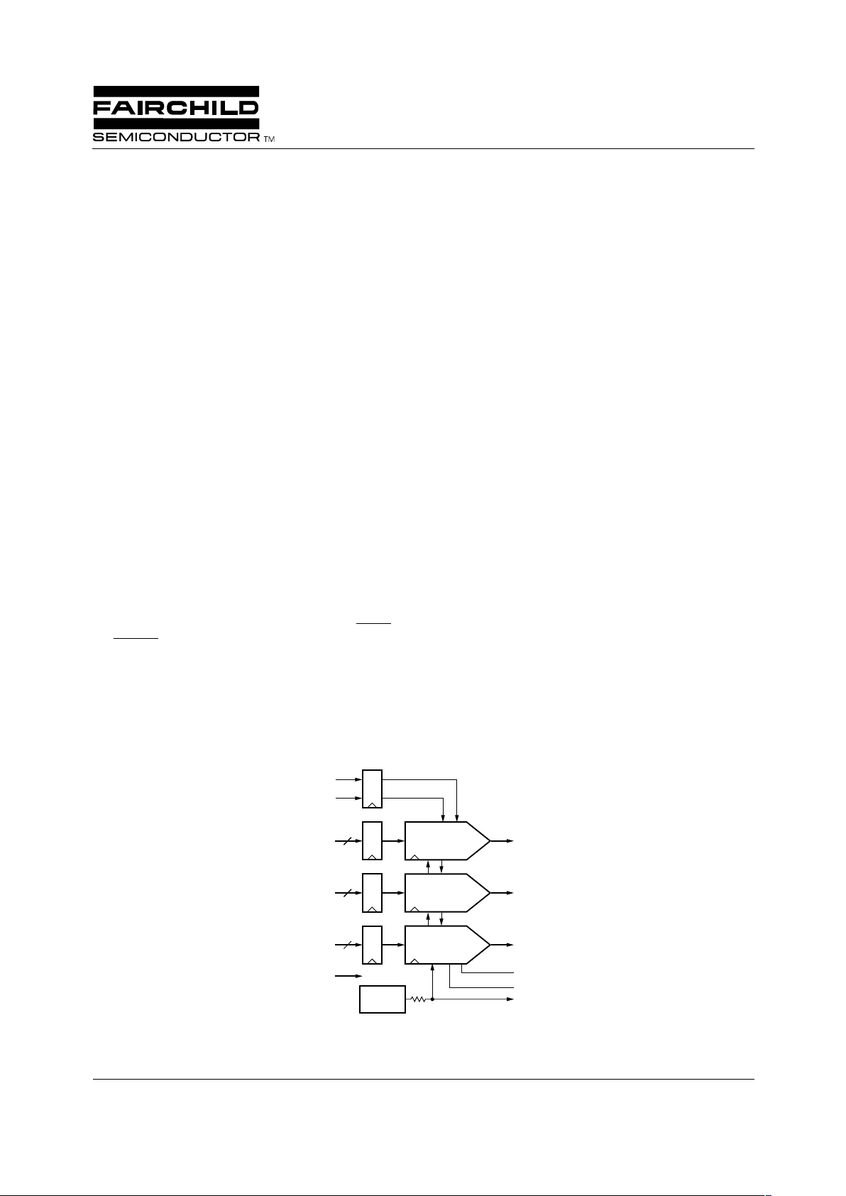
Block Diagram
10 bit
D/A Converter
10 bit
D/A Converter
10 bit
D/A Converter
10
G
9-0
BLANK
SYNC
CLK
IO
G
IO
B
IO
R
V
REF
R
REF
COMP
65-3003-01
+1.235V
Ref
10
B
9-0
10
R
9-0
Description
The TMC3003 is a high-speed triple 10-bit D/A converter
especially suited for video and graphics applications.
It offers 10-bit resolution, TTL-compatible inputs, low
power consumption, and requires only a single +5 Volt
power supply. It has single-ended current outputs, SYNC
and BLANK control inputs, and a separate current source for
adding sync pulses to the Green D/A converter output. It is
ideal for generating analog RGB from digital RGB and
driving computer display and video monitors. Three speed
grades are available: 30, 50, and 80 Msps.
The TMC3003 triple D/A converter is available in a 44-lead
plastic J-leaded PLCC and 48-Lead quad flatpack (LQFP).
It is fabricated on a sub-micron CMOS process with performance guaranteed from 0°C to 70°C.
TMC3003
Triple Video D/A Converter
10 bit, 80 Msps
Page 2
TMC3003 PRODUCT SPECIFICATION
2
2
REV. 1.0.3 3/5/01
Functional Description
The TMC3003 is a low-cost triple 10-bit CMOS D/A
converter designed to directly drive computer CRT displays
and video transmission lines at pixel rates of up to 80 Msps.
It comprises three identical 10-bit D/A converters with
registered data inputs, common clock, and internal voltage
reference. An independent current source allows sync to be
added to the green D/A converter output.
Digital Inputs
All digital inputs are TTL-compatible. Data are registered on
the rising edge of the CLK signal. The analog output
changes t
DO
after the rising edge of CLK. There is one stage
of pipeline delay on the chip. The guaranteed clock rates of
the TMC3003 are 80, 50, and 30 MHz.
SYNC
and BLANK
SYNC and BLANK inputs control the output level
(Figure 1 and Table 1) of the D/A converters during CRT
retrace intervals. BLANK forces the D/A outputs to the
blanking level while SYNC turns off a separate current
source which is connected to the green D/A converter. This
connection adds a 40 IRE sync pulse to the D/A output and
brings that D/A output to 0.0 Volts during the sync tip.
SYNC and BLANK are registered on the rising edge of
CLK.
BLANK gates the D/A inputs and sets the pedestal voltage.
If BLANK = HIGH, the D/A inputs are added to a pedestal
which offsets the current output. If BLANK = LOW, data
inputs and the pedestal are disabled.
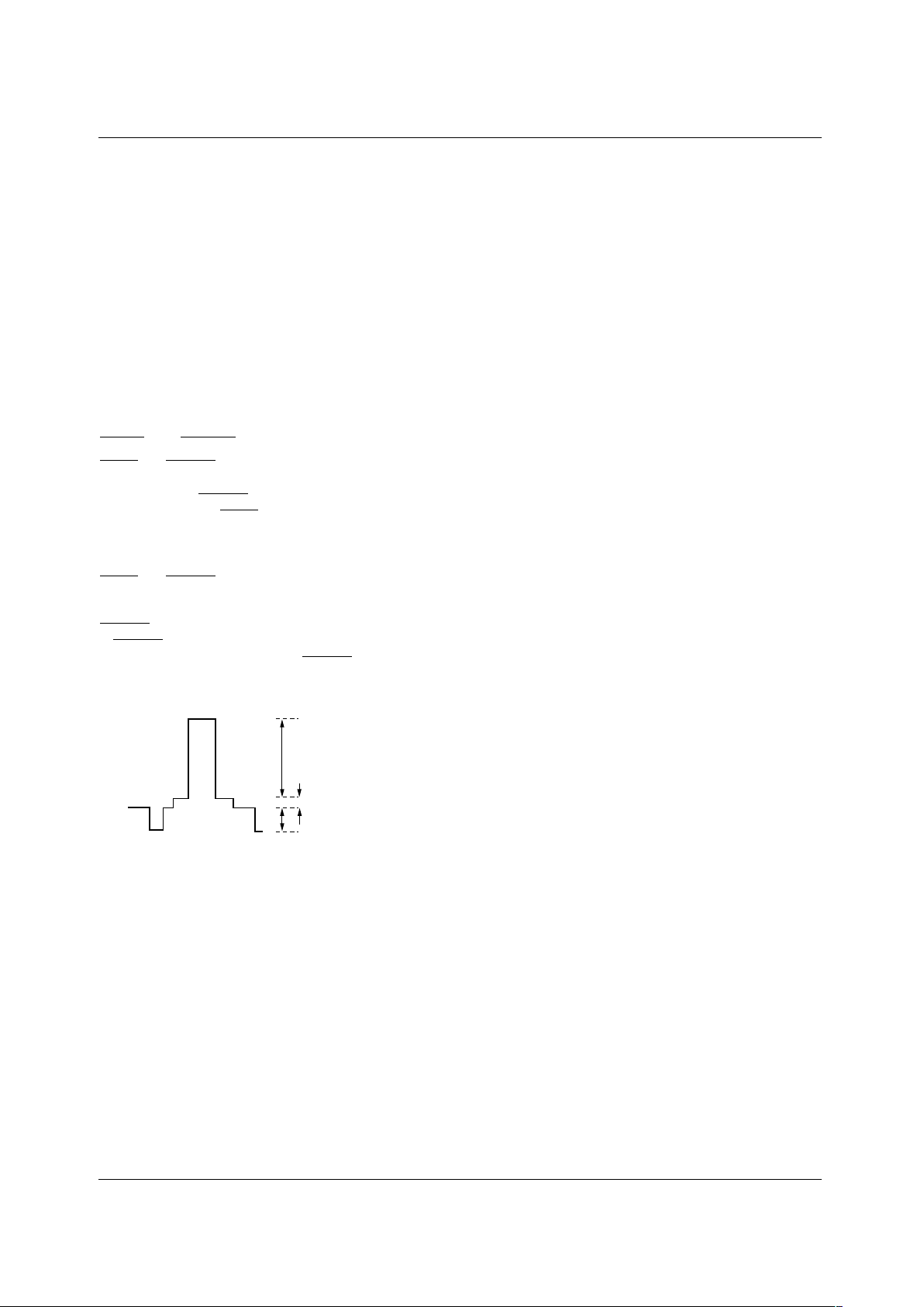
Figure 1. Nominal Output Levels
data: 660 mV max.
65-3003-02
pedestal: 54 mV
sync: 286 mV
D/A Outputs
Each D/A output is a current source. To obtain a voltage output a resistor must be connected to ground. Output voltage of
the D/A converters depends upon this resistor, the reference
voltage, and the value of the gain-setting resistor connected
between R
REF
and GND.
Normally, a source termination resistor of 75 Ohms is connected between the D/A current output pin and GND near
the D/A converter. A 75 Ohm coaxial cable may then be connected with another 75 Ohm termination resistor at the far
end of the cable. This “double termination” presents the D/A
converter with a net resistive load of 37.5 Ohms.
The TMC3003 may also be operated with a single 75 Ohm
terminating resistor. To lower the output voltage swing to the
desired range, the value of the resistor on R
REF
should be
increased.
Voltage Reference
The TMC3003 has an internal bandgap voltage reference
of +1.235 Volts. An external voltage reference may be
connected to the V
REF
pin, overriding the internal voltage
reference. All three D/A converters are driven from the same
reference.
A 0.1µF capacitor must be connected between the COMP
pin and V
DD
to stabilize internal bias circuitry and ensure
low-noise operation.
Power and Ground
The TMC3003 D/A converter requires a single +5.0 Volt
power supply. The analog (V
DD
) power supply voltage
should be decoupled to GND to reduce power supply
induced noise. 0.1µF decoupling capacitors should be placed
as close as possible to the power pins.
The high slew-rate of digital data makes capacitive coupling
to the outputs of any D/A converter a potential problem.
Since the digital signals contain high-frequency components
of the CLK signal, as well as the video output signal, the
resulting data feedthrough often looks like harmonic distortion or reduced signal-to-noise performance. All ground pins
should be connected to a common solid ground plane for
best performance.
Page 3
PRODUCT SPECIFICATION TMC3003
REV. 1.0.3 3/5/01
3
Table 1. Output Voltage versus Input Code, SYNC
, and BLANK
V
REF
= 1.235 V, R
REF
= 590 Ω , R
L
= 37.5 Ω
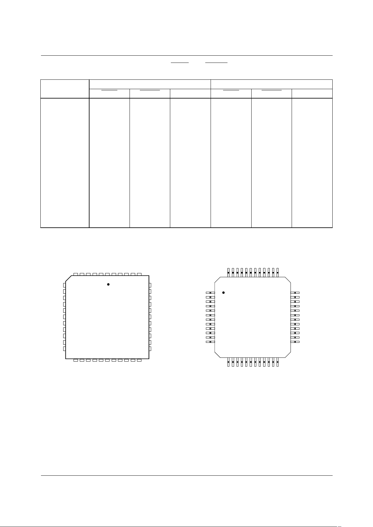
Pin Assignments
RGB
9-0
(MSB...LSB)
Red and Blue D/As Green D/A
SYNC BLANK V
OUT
SYNC BLANK V
OUT
11 1111 1111 X 1 0.7140 1 1 1.0000
11 1111 1110 X 1 0.7134 1 1 0.9994
11 1111 1101 X 1 0.7127 1 1 0.9987
• ••••••
• ••••••
10 0000 0000 X 1 0.3843 1 1 0.6703
01 1111 1111 X 1 0.3837 1 1 0.6697
• ••••••
• ••••••
00 0000 0010 X 1 0.0553 1 1 0.3413
00 0000 0001 X 1 0.0546 1 1 0.3406
00 0000 0000 X 1 0.0540 1 1 0.3400
xx xxxx xxxx X 0 0.0000 1 0 0.2860
xx xxxx xxxx X 0 0.0000 0 0 0.0000
65-3003-03
G
1
G
2
G
3
G
4
G
5
G
6
G
7
G
8
G
9
BLANK
SYNC
R
REF
V
REF
COMP
IO
R
IO
G
V
DD
V
DD
IO
B
GND
GND
CLK
G0R9R8R7R6R5R4R3R2R1R
0
V
DD
B0B1B2B3B4B5B6B7B8B
9
7
8
9
10
11
12
13
14
15
16
17
39
38
37
36
35
34
33
32
31
30
29
1819202122232425262728
65432
1
4443424140
TMC3003
65-3003-05
G
1
G
2
G
3
G
4
G
5
G
6
G
7
G
8
G
9
BLANK
V
DD
R2R1NC
R
REF
V
REF
COMP
IO
G
IO
R
OV
DD
V
DD
IO
B
GND
GND
NC
G0R9R8R7R6R5R4R
3
NC
B
0B1B2B3B4B5B6B8B7
NC
1
2
3
4
5
6
7
8
9
10
SYNC
11
12
36
35
34
33
32
31
30
29
28
27
CLOCK
26
25
131415161718192021
22
B
9
23
24
484746454443424140
39
R
0
38
37
TMC3003
LQFPPLCC
Page 4
TMC3003 PRODUCT SPECIFICATION
4
REV. 1.0.3 3/5/01
Pin Descriptions
Pin Name
Pin Number
Value DescriptionPLCC LQFP
Clock and Pixel I/O
CLK 29 26 TTL
Clock. The clock input is TTL-compatible and all pixel data
is registered on the rising edge of CLK. It is recommended
that CLK be driven by a dedicated TTL buffer to avoid
reflection induced jitter, overshoot, and undershoot.
R
9-0
5, 4, 3, 2, 1,
44, 43, 42,
41, 40
47, 46, 45,
44, 43, 42,
41, 40, 39,
38, 37
TTL
Red pixel data inputs. The Red digital input is TTL-
compatible and registered on the rising edge of CLK.
G
9-0
15, 14, 13,
12, 11, 10, 9,
8, 7, 6
48, 9, 8, 7, 6,
5, 4, 3, 2, 1
TTL
Green pixel data inputs. The Green digital input is TTL-
compatible and registered on the rising edge of CLK.
B
9-0
28, 27, 26,
25, 24, 23,
22, 21, 20,
19
23, 22, 21,
20, 19, 18,
17, 16, 15,
14
TTL
Blue pixel data inputs. The Blue digital input is TTL-
compatible and registered on the rising edge of CLK.
Controls
SYNC 17 11 TTL
Sync pulse Input. Bringing SYNC LOW, turns off a 40
IRE (7.62 mA) current source which forms a sync pulse on
the Green D/A converter output. SYNC is registered on the
rising edge of CLK along with pixel data and has the same
pipeline latency as BLANK and pixel data. SYNC does not
override any other data and should be used only during
the blanking interval.
Since this is a single-supply D/A and all signals are
positive-going, sync is added to the bottom of the Green
D/A range. So turning SYNC OFF means turning the
current source ON. When a sync pulse is desired, the
current source is turned OFF. If the system does not
require sync pulses from the Green D/A converter, SYNC
should be connected to GND.
BLANK 16 10 TTL
Blanking Input. When BLANK is LOW, pixel inputs are
ignored and the D/A converter outputs are driven to the
blanking level. BLANK is registered on the rising edge of
CLK and has the same pipeline latency as SYNC.
Video Outputs
IO
R
36 33 0.714 Vp-p Red D/A output. The current source outputs of the D/A
converters are capable of driving RS-343A/SMPTE-170M
compatible levels into doubly-terminated 75 Ohm lines.
IO
G
35 32 1 V p-p Green D/A output. The current source outputs of the D/A
converters are capable of driving RS-343A/SMPTE-170M
compatible levels into doubly-terminated 75 Ohm lines.
Sync pulses may be added to the Green D/A output.
IO
B
32 29 0.714 Vp-p Blue D/A output. The current source outputs of the D/A
converters are capable of driving RS-343A/SMPTE-170M
compatible levels into doubly-terminated 75 Ohm lines.
Page 5

PRODUCT SPECIFICATION TMC3003
REV. 1.0.3 3/5/01
5
Equivalent Circuits
Figure 2. Equivalent Digital Input Circuit Figure 3. Equivalent Analog Output Circuit
Voltage Reference
V
REF
38 35 +1.235 V Voltage Reference output/input. An internal voltage
source of +1.235 Volts is output on this pin. An external
+1.235 Volt reference may be applied here which
overrides the internal reference. Decoupling V
REF
to GND
with a 0.1µF ceramic capacitor is required.
R
REF
39 36 560 Ω
Current-setting resistor. The full-scale output current of
each D/A converter is determined by the value of the
resistor connected between R
REF
and GND. The nominal
value for R
REF
is found from:
R
REF
= 9.1( V
REF
/I
FS
)
where I
FS
is the full-scale (white) output current (in amps)
from the
D/A converter (without sync). Sync is 0.4 * I
FS
.
D/A full-scale (white) current may also be calculated from:
I
FS
= V
FS
/ R
L
Where V
FS
is the white voltage level and R
L
is the total
resistive load (in ohms) on each D/A converter. V
FS
is the
blank to full-scale voltage.
COMP 37 34 0.1 µF Compensation capacitor. A 0.1 µF ceramic capacitor
must be connected between COMP and V
DD
to stabilize
internal bias circuitry.
Power and Ground
V
DD
18, 33, 34 12, 30, 31 +5 V Power supply
GND 30, 31 27, 28 0.0 V Ground
Pin Descriptions
(continued)
Pin Name
Pin Number
Value DescriptionPLCC LQFP
Digital
Input
V
DD
p
n
27014C
GND
np
OUT
GND
27013B
V
DD
V
DD
Page 6

TMC3003 PRODUCT SPECIFICATION
6
REV. 1.0.3 3/5/01
Equivalent Circuits
(continued)
Figure 4. Equivalent Analog Input Circuit
Absolute Maximum Ratings
(beyond which the device may be damaged)
1
Notes:
1. Functional operation under any of these conditions is NOT implied. Performance and reliability are guaranteed only if
Operating Conditions are not exceeded.
2. Applied voltage must be current limited to specified range.
3. Forcing voltage must be limited to specified range.
4. Current is specified as conventional current flowing into the device.
Parameter Min Typ Max Unit
Power Supply Voltage
V
DD
(Measured to GND) -0.5 7.0 V
Inputs
Applied Voltage (measured to GND)
2
-0.5 V
DD
+ 0.5 V
Forced Current
3,4
-10.0 10.0 mA
Outputs
Applied Voltage (measured to GND)
2
-0.5 VDD + 0.5 V
Forced Current
3,4
-60.0 60.0 mA
Short Circuit Duration (single output in HIGH state to ground) infinite second
Temperature
Operating, Ambient -20 110 °C
Junction 150 °C
Lead Soldering (10 seconds) 300 °C
Vapor Phase Soldering (1 minute) 220 °C
Storage -65 150 °C
p
GND
27012B
R
REF
V
REF
V
DD
p
Page 7

PRODUCT SPECIFICATION TMC3003
REV. 1.0.3 3/5/01 7
Operating Conditions
Electrical Characteristics
Notes:
1. Values shown in Typ column are typical for V
DD
= +5V and TA = 25°C.
2. Minimum/Maximum values with V
DD
= Max and TA = Min.
3. V
REF
= 1.235V, R
LOAD
= 37.5Ω, R
REF
= 540Ω
Parameter Min Nom Max Units
V
DD
Power Supply Voltage 4.75 5.0 5.25 V
f
S
Conversion Rate TMC3003-30 30 Msps
TMC3003-50 50 Msps
TMC3003-80 80 Msps
t
PWH
CLK Pulsewidth, HIGH 4 ns
t
PWL
CLK Pulsewidth, LOW 4 ns
t
s
Input Data Setup Time 3 ns
t
h
Input Date Hold Time 2 ns
V
REF
Reference Voltage, External 1.0 1.235 1.5 V
C
C
Compensation Capacitor 0.1 µF
R
L
Output Load 37.5 Ω
V
IH
Input Voltage, Logic HIGH 2.0 V
DD
V
V
IL
Input Voltage, Logic LOW GND 0.8 V
T
A
Ambient Temperature, Still Air 0 70 °C
Parameter Conditions
3
Min Typ
1
Max Units
I
DD
Power Supply Current
2
VDD = Max
TMC3003-30 100 mA
TMC3003-50 100
TMC3003-80 125
PD Total Power Dissipation
2
V
DD
= Max
TMC3003-30 525 mW
TMC3003-50 525
TMC3003-80 655
R
O
Output Resistance 100 kΩ
C
O
Output Capacitance I
OUT
= 0mA 30 pF
I
IH
Input Current, HIGH VDD = Max, VIN = 2.4V -1 µA
I
IL
Input Current, LOW VDD = Max, VIN = 0.4V 1 µA
I
REF
V
REF
Input Bias Current 0 ±100 µA
V
REF
Reference Voltage Output 1.235 V
V
OC
Output Compliance Referred to V
DD
-0.4 0 +1.5 V
C
DI
Digital Input Capacitance 4 10 pF
Page 8

TMC3003 PRODUCT SPECIFICATION
8 REV. 1.0.3 3/5/01
Switching Characteristics
Notes:
1. Values shown in Typ column are typical for V
DD
= +5V and TA = 25°C.
2. V
REF
= 1.235V, R
LOAD
= 37.5Ω, R
REF
= 590Ω.
System Performance Characteristics
Notes:
1. Values shown in Typ column are typical for V
DD
= +5V and TA = 25°C.
2. V
REF
= 1.235V, R
LOAD
= 37.5Ω, R
REF
= 590Ω.
Timing Diagram
Parameter Conditions
2
Min Typ
1
Max Units
t
D
Clock to Output Delay VDD = Min 10 15 ns
t
SKEW
Output Skew 1 2 ns
t
R
Output Risetime 10% to 90% of Full Scale 2 3 ns
t
F
Output Falltime 90% to 10% of Full Scale 2 3 ns
t
SET
Output Settling Time to 3%/FS 15 ns
Parameter Conditions
2
Min Typ
1
Max Units
E
LI
Integral Linearity Error VDD, V
REF
= Nom ±0.1 ±0.25 %/FS
E
LD
Differential Linearity Error VDD, V
REF
= Nom ±0.1 ±0.25 %/FS
E
DM
DAC to DAC Matching VDD, V
REF
= Nom 3 10 %
E
G
Absolute Gain Error VDD, V
REF
= Nom — %/FS
TC
E
Gain Error Tempco VDD, V
REF
= Nom — PPM/°C
V
OF
Output Offset Current VDD = Max, R, G, B = 000h 20 mA
PSR Power Supply Rejection 0.05 %/%
CLK
PIXEL DATA
& CONTROLS
OUTPUT
65-3003-03
DataN DataN+1 DataN+2
t
PWL
t
S
t
H
50%
3%/FS
90%
10%
t
D
t
SET
t
F
t
R
t
PWH
1/f
S
Page 9

PRODUCT SPECIFICATION TMC3003
REV. 1.0.3 3/5/01 9
Applications Discussion
Figure 4 illustrates a typical TMC3003 interface circuit.
In this example, an optional 1.2 Volt bandgap reference is
connected to the V
REF
output, overriding the internal volt-
age reference source.
Grounding
It is important that the TMC3003 power supply is wellregulated and free of high-frequency noise. Careful power
supply decoupling will ensure the highest quality video signals at the output of the circuit. The TMC3003 has separate
analog and digital circuits. To keep digital system noise from
the D/A converter, it is recommended that power
supply voltages (V
DD
) come from the system analog power
source and all ground connections (GND) be made to the
analog ground plane. Power supply pins should be individually decoupled at the pin.
Printed Circuit Board Layout
Designing with high-performance mixed-signal circuits
demands printed circuits with ground planes. Overall
system performance is strongly influenced by the board layout. Capacitive coupling from digital to analog circuits may
result in poor D/A conversion. Consider the following
suggestions when doing the layout:
1. Keep the critical analog traces (V
REF
, I
REF
, COMP,
IOR, IOG, IOB) as short as possible and as far as possible from all digital signals. The TMC3003 should be
located near the board edge, close to the analog output
connectors.
2. The power plane for the TMC3003 should be separate
from that which supplies the digital circuitry. A single
power plane should be used for all of the V
DD
pins. If
the power supply for the TMC3003 is the same as that of
the system's digital circuitry, power to the TMC3003
should be decoupled with 0.1µF and 0.01µF capacitors
and isolated with a ferrite bead.
3. The ground plane should be solid, not cross-hatched.
Connections to the ground plane should have very short
leads.
4. If the digital power supply has a dedicated power plane
layer, it should not be placed under the TMC3003, the
voltage reference, or the analog outputs. Capacitive coupling of digital power supply noise from this layer to the
TMC3003 and its related analog circuitry can have an
adverse effect on performance.
5. CLK should be handled carefully. Jitter and noise on
this clock will degrade performance. Terminate the
clock line carefully to eliminate overshoot and ringing.
Related Products
• TMC3503 Triple 8-bit 80 Msps D/A Converters
• TMC1175A 40 Msps CMOS 8-bit A/D Converter
• TMC1275 40 Msps CMOS 8-bit A/D Converter
• TMC22091, TMC22191 Digital Video Encoders
• TMC2242A/TMC2243/TMC2246A Video Filters
• TMC2249A Digital Mixer
• TMC2250A Matrix Multiplier
• TMC2272A Colorspace Converter
• TMC2302 Image Manipulation Sequencer
• TMC2340A Digital Synthesizer
• TMC2081 Digital Video Mixer
Figure 4. Typical Interface Circuit
65-3003-04
R
9-0
G
9-0
B
9-0
+5V
0.1µF
10µF
V
DD
GND
TMC3003
Triple 10-bit
D/A Converter
CLK
SYNC
BLANK
RED PIXEL
INPUT
GREEN PIXEL
INPUT
BLUE PIXEL
INPUT
CLOCK
SYNC
BLANK
COMP
V
REF
R
REF
+5V
0.1µF
0.1µF
560Ω
3.3kΩ
LM185-1.2
(Optional)
IO
R
IO
G
IO
B
75Ω
75Ω
75Ω
75Ω
75Ω
75Ω
ZO=75Ω
ZO=75Ω
ZO=75Ω
Red
Green
Blue
Page 10

TMC3003 PRODUCT SPECIFICATION
10 REV. 1.0.3 3/5/01
Mechanical Dimensions – 44-Lead PLCC Package
D
e
E
A .165 .180 4.19 4.57
Symbol
Inches
Min. Max. Min. Max.
Millimeters
Notes
E1
J
D1
A
A1
A2
B
B1
D3/E3
J
– C –
ccc C
LEAD COPLANARITY
A1 .090 .120 2.29 3.05
A2 .020 .51——
B .013 .021 .33 .53
D/E .685 .695 17.40 17.65
D1/E1 .650 .656 16.51 16.66
D3/E3 .500 BSC 12.7 BSC
e .050 BSC 1.27 BSC
J .042 .056 1.07 1.42 2
3
ND/NE 11 11
N44 44
ccc .004 0.10——
B1 .026 .032 .66 .81
Notes:
1.
2.
3.
All dimensions and tolerances conform to ANSI Y14.5M-1982
Corner and edge chamfer (J) = 45°
Dimension D1 and E1 do not include mold protrusion. Allowable
protrusion is .101" (.25mm)
Page 11

PRODUCT SPECIFICATION TMC3003
REV. 1.0.3 3/5/01 11
Mechanical Dimensions – 48-Lead LQFP Package
D
E1
E
e
PIN 1
IDENTIFIER
B
Base Plane
Seating Plane
See Lead Detail
C
0.063" Ref (1.60mm)
L
-C-
ccc
C
LEAD COPLANARITY
A2
A
A1
α
A .055 .063 1.40 1.60
Symbol
Inches
Min. Max. Min. Max.
Millimeters
Notes
A1 .001 .005 .05 .15
.057 1.45
A2 .053 1.35
B .006 .010 .17 .27
D/E
D1/E1
.019 BSC
.346 .362 8.8 9.2
.268 .284 6.8 7.2
.50 BSC
e
L .017 .029 .45 .75 6
4
5
2
7
8
α 0° 7° 0° 7°
N48 48
12 12
ND
ccc .004 0.08
Notes:
1.
2.
3.
4.
5.
6.
7.
8.
D1
All dimensions and tolerances conform to ANSI Y14.5M-1982.
Dimensions "D1" and "E1" do not include mold protrusion.
Allowable protrusion is 0.25mm per side. D1 and E1 are maximum
plastic body size dimensions including mold mismatch.
Pin 1 identifier is optional.
Dimension ND: Number of terminals.
Dimension ND: Number of terminals per package edge.
"L" is the length of terminal for soldering to a substrate.
Dimension "B" does not include dambar protrusion. Allowable
dambar protrusion shall not cause the lead width to exceed the
maximum B dimension by more than 0.08mm. Dambar can not be
located on the lower radius or the foot. Minimum space between
protrusion and an adjacent lead is 0.07mm for 0.4mm and 0.5mm
pitch packages.
To be determined at seating place —C—
Page 12

TMC3003 PRODUCT SPECIFICATION
3/5/01 0.0m 002
Stock#DS30003003
2001 Fairchild Semiconductor Corporation
LIFE SUPPORT POLICY
FAIRCHILD’S PRODUCTS ARE NOT AUTHORIZED FOR USE AS CRITICAL COMPONENTS IN LIFE SUPPORT DEVICES
OR SYSTEMS WITHOUT THE EXPRESS WRITTEN APPROVAL OF THE PRESIDENT OF FAIRCHILD SEMICONDUCTOR
CORPORATION. As used herein:
1. Life support devices or systems are devices or systems
which, (a) are intended for surgical implant into the body,
or (b) support or sustain life, and (c) whose failure to
perform when properly used in accordance with
instructions for use provided in the labeling, can be
reasonably expected to result in a significant injury of the
user.
2. A critical component in any component of a life support
device or system whose failure to perform can be
reasonably expected to cause the failure of the life support
device or system, or to affect its safety or effectiveness.
www.fairchildsemi.com
Ordering Information
Product Number
Conversion
Rate (Msps)
Temperature
Range Screening Package
Package
Marking
TMC3003R2C30 30 Msps T
A
= 0°C to 70°C Commercial 44-Lead PLCC 3003R2C30
TMC3003R2C50 50 Msps T
A
= 0°C to 70°C Commercial 44-Lead PLCC 3003R2C50
TMC3003R2C80 80 Msps TA = 0°C to 70°C Commercial 44-Lead PLCC 3003R2C80
TMC3003KRC30 30 Msps T
A
= 0°C to 70°C Commercial 48-Lead LQFP 3003KRC30
TMC3003KRC50 50 Msps T
A
= 0°C to 70°C Commercial 48-Lead LQFP 3003KRC50
TMC3003KRC80 80 Msps TA = 0°C to 70°C Commercial 48-Lead LQFP 3003KRC80
DISCLAIMER
FAIRCHILD SEMICONDUCTOR RESERVES THE RIGHT TO MAKE CHANGES WITHOUT FURTHER NOTICE TO
ANY PRODUCTS HEREIN TO IMPROVE RELIABILITY, FUNCTION OR DESIGN. FAIRCHILD DOES NOT ASSUME
ANY LIABILITY ARISING OUT OF THE APPLICATION OR USE OF ANY PRODUCT OR CIRCUIT DESCRIBED HEREIN;
NEITHER DOES IT CONVEY ANY LICENSE UNDER ITS PATENT RIGHTS, NOR THE RIGHTS OF OTHERS.
 Loading...