

Page 1
www.fairchildsemi.com
Features
• TMC2242A and TMC2242B are pin-compatible with
TMC2242
• User selectable interpolate gain, -6 dB or 0 dB (2242B)
• 30, 40 and 60 MHz speed grades
• User selectable 2:1 decimation, 1:2 interpolation, and
equal-rate filter modes
• Passband ripple <
±
0.01 dB
• Stopband rejection 59.4 dB from 0.28 to 0.50 x f
s
• Cascading two TMC2242A or TMC2242B meets
CCIR 601 low-pass filter requirement
• Dedicated 12-bit 2's complement input data port and
16-bit output data port with user-selectable rounding from
9 to 16 bits
• Two's complement or offset binary output format
• Built-in limiter prevents overflow
• Single +5 Volt power supply operation
• Small 44-Lead PLCC and 44-Lead MQFP
Applications
• Low-cost video filtering
• Chrominance bandwidth limiter
• Simple, inexpensive video D/A post-filters
• Reduced cost and complexity for A/D anti-aliasing filters
• High-performance digital low-pass filters
• Digital waveform reconstruction post-filtering
• Telecommunications
• Direct digital synthesis
• Radar
Description
The TMC2242A and TMC2242B are fixed-coefficient linear-phase half-band (low-pass) digital filters. They can be
used to halve or double the sampling rate of a digital signal.
When used as a decimating post-filter with a double-speed
oversampling A/D con verter , they greatly reduce the cost and
complexity of anti-aliasing filters required ahead of the A/D
converter. When used as an interpolating pre-filter with a
double-speed oversampling D/A converter, the TMC2242A
and TMC2242B significantly reduce the design complexity
and production cost of reconstruction filters used on D/A
outputs.
The TMC2242A and TMC2242B user selects the mode of
operation (decimate, interpolate, or equal-rate) and rounding. The TMC2242A and TMC2242B accept 12-bit 2's complement data at up to 60 MHz and output saturated
(overflow-protected) 2's complement or offset binary data
rounded to from 9 to 16 bits. Within the speed grade I/O
limit, the output sample rate may be 1/2, 1, or 2 times the
input sample rate.
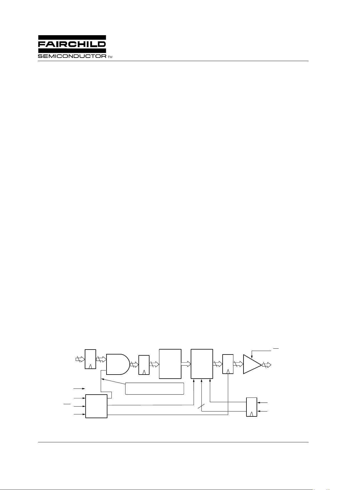
Block Diagram
SI
11-0
CLK
DEC
INT
SYNC
12
12
12
12 16
16
16
SO
15-0
TCO
RND
2-0
55 Tap
FIR
Filter
Round
and
Limit
3
Control
OE
Interpolate 0-1-0-1
Decimate, Equal Rate 1-1-1-1
65-2242A-01
TMC2242A/TMC2242B
Digital Half-Band Interpolating/Decimating Filter
12-bit In/16-bit Out, 60 MHz
Rev. 1.2.0
Page 2

PRODUCT SPECIFICATION TMC2242A/TMC2242B
2
The filter response is flat to within
±
0.01 dB from 0.00 to
0.22 x f
s
, with stopband attenuation greater than 59.4 dB
from 0.28 x f
s
to the Nyquist frequency . The response is 6 dB
down at 0.25 x f
s
. Symmetric-coefficient filters such as the
TMC2242A and TMC2242B have linear phase response.
Full compliance with the CCIR-601 standard of 12 dB attenuation at 0.25 x f
s
is achieved by cascading two parts.
The TMC2242A and TMC2242B are fabricated on an
advanced submicron CMOS process. They are available in a
44-lead J-lead PLCC package. Performance is guaranteed
from 0
°
C to 70
°
C.
Functional Description
The TMC2242A and TMC2242B implement a fixed-coefficient linear-phase Finite Impulse Response (FIR) filter of 55
effective taps, with special rate-matching input and output
structures to facilitate 2:1 decimation and 1:2 interpolation.
The faster of either the input or output registers will operate
at the guaranteed maximum clock rate (speed grade). The
total internal pipeline latency from the input of an impulse to
the corresponding output peak (digital group delay) is 34
cycles; the 55-value output response begins after 7 clock
cycles and ends after 61 cycles.
To perform interpolation, the chip slows the effective input
register clock rate to half the output rate. It internally inserts
zeroes between the incoming data samples to "pad" the input
data rate to match the output rate.
To perform decimation, the chip sets the output register
clock rate to half of the input rate. One output is then
obtained for every two inputs.
For interpolation, the user should bring SYNC HIGH for at
least one clock cycle, returning it LOW with the first desired
input data value. When interpolating, the chip will then continue to accept a new data input on each alternate rising edge
of the clock. When decimating, the chip will present one output value for every two clock cycles. The user may leave
SYNC LOW or toggle it once per rising clock edge, with
equivalent performance.
The output data format is two's complement if TCO is
HIGH, inverted of fset binary if LOW. The user can tailor the
output data word width to his/her system requirements using
the Rounding control. As shown in Table 4, the output is
half-LSB rounded to the resolution selected by the value of
RND
2-0
. The asynchronous three-state output enable control
simplifies connection to a data bus with other drivers.
Table 1. Operating Modes
Note:
1. With 15-bit overflow protection. All other modes on both
parts limit to 16 bits.
DEC
INT TMC2242A TMC2242B
0 0 Equal Rate Interpolate (0 dB)
0 1 Decimate Decimate
1 0 Interpolate (-6 dB) Interpolate (-6 dB)
1
1 1 Equal Rate Equal Rate
Pin Assignments
65-2242A-02
SO
12
SO
11
SO
10
SO
9
SO
8
GND
V
DD
SO
7
SO
6
SO
5
SO
4
GND
V
DD
SI
10
SI
9
SI
8
SI
7
SI
6
SI
5
SI
4
SI
3
V
DD
SO13SO14SO15OE
TCO
DEC
INT
SYNC
CLK
GND
SI
11
SO3SO2SO1SO
0
RND2RND1RND
0
SI0SI1SI
2
GND
7
8
9
10
11
12
13
14
15
16
17
39
38
37
36
35
34
33
32
31
30
29
1819202122232425262728
65432
1
4443424140
TMC2242A
TMC2242B
65-2242A-02
SO
12
SO
11
SO
10
SO
9
SO
8
GND
V
DD
SO
7
SO
6
SO
5
SO
4
GND
V
DD
SI
10
SI
9
SI
8
SI
7
SI
6
SI
5
SI
4
SI
3
V
DD
SO13SO14SO15OE
TCO
DEC
INT
SYNC
CLK
GND
SI
11
SO3SO2SO1SO
0
RND2RND1RND
0
SI0SI1SI
2
GND
1
2
3
4
5
6
7
8
9
10
11
33
32
31
30
29
28
27
26
25
24
23
1213141516171819202122
4443424140393837363534
TMC2242A
TMC2242B
Description
(continued)
44 Lead PLCC
44 Lead MQFP
Page 3
TMC2242A/TMC2242B PRODUCT SPECIFICATION
3
Pin Descriptions
Pin Name
Pin Number
Pin Function DescriptionPLCC MQFP
Timing Controls
INT
44 38
Interpolate. When INT is LOW and DEC is HIGH, the input data register runs at
1/2 the CLK rate and zeros are inserted in the data stream between valid input
values, reducing gain by 6dB. The TMC2242A and TMC2242B interpolate and
output results at the full CLK rate.
DEC 139 Decimate. When DEC is LOW and INT is HIGH, the input data register runs at
the full CLK rate. In this mode, the TMC2242A and TMC2242B decimate and
output results at 1/2 the CLK rate.
When INT
= DEC, the TMC2242A is in equal rate mode. When both INT and DEC
are HIGH, the TMC2242B is likewise in equal-rate mode, but when both INT and
DEC are LOW, the TMC2242B interpolates with unity gain.
In equal-rate mode, the input and output sample rates equal the chip clock rate.
SYNC 43 37
Synchronization. Incoming data are synchronized by holding SYNC HIGH on
CLK N–1 and LOW on CLK N when the first input data word is present on SI
11-0
.
If DEC
= INT=1 (equal rate mode), SYNC is inactive. SYNC may be held LOW
until resynchronization is desired, or it may be toggled at 1/2 the CLK rate.
CLK 42 36
Clock. The TMC2242A and TMC2242B operate from a single master clock. All
internal registers, except the output register in decimation mode, are strobed on
the rising edge of CLK. All timing parameters are referenced to the rising edge of
CLK.
Data Inputs
SI
11-0
40,
37-30,
27-25
34,
31-24,
21-19
Input Data Port. A 12-bit 2's-complement input word is registered by the rising
edge of CLK. In Interpolate Mode, SI
11-0
is registered on every other CLK
(synchronized by SYNC). SI
11
is the MSB.
Data Outputs
SO
15-0
4-11,
14-21
42-44,
1-5,
8-15
Output Data Port. A 16-bit 2's-complement output result is available after the
rising edge of CLK. In Decimate Mode, SO
15-0
is registered on every other CLK
(synchronized by SYNC). SO
15-0
is rounded according to the state of RND
2-0
.
SO
15
is the MSB.
The limiter circuitry ensures that for internal overflow, a valid full-scale output
(7FFF or 8000) will be generated. With the TMC2242B in interpolate mode with
-6dB gain, limits are 3FFF and C000 (TCO=1).
Output Controls
OE
341 Output Enable. When LOW, SO
15-0
are enabled. When HIGH, SO
15-0
are in a
high-impedance state. OE
is asynchronous with respect to CLK.
TCO 2 40
Output Format. When TCO is HIGH, output data are in signed 2's-complement
format. When LOW, the output is inverted offset binary.
RND
2-0
22-24 16-18 Rounding Select. These inputs set the position of the effective LSB of the output
result. Outputs below the rounding bit are zeroed (Table 4).
Power
V
DD
13,29,387, 23,
32
Supply Voltage. +5 Volt power inputs. These should come from the same power
source and be decoupled to GND.
GND 12,28,
39,41
6, 22,
33, 35
Ground. Ground inputs should be connected to the system digital ground plane.
Page 4
PRODUCT SPECIFICATION TMC2242A/TMC2242B
4
Absolute Maximum Ratings
(beyond which the device may be damaged)
1
Notes:
1. Functional operation under any of these conditions is NOT implied. Performance and reliability are guaranteed only if
Operating Conditions are not exceeded.
2. Applied voltage must be current limited to specified range.
3. Forcing voltage must be limited to specified range.
4. Current is specified as conventional current flowing into the device.
Operating Conditions
Parameter Conditions Min Max Units
Supply Voltage -0.5 7.0 V
Input Voltage -0.5 V
DD
+ 0.5 V
Output Applied Voltage
2
-0.5 V
DD
+ 0.5 V
Externally Forced Current
3,4
-3.0 +6.0 mA
Short Circuit Duration Single output in HIGH state to ground 1 sec
Operating Temperature (Case) -20 110
°
C
Junction Temperature 140
°
C
Lead Soldering Temperature 10 seconds 300
°
C
Storage Temperature -65 150
°
C
Parameter Conditions Min Nom Max Units
V
DD
Power Supply Voltage 4.75 5.0 5.25 V
f
CLK
Clock frequency TMC2242A, B 30 MHz
TMC2242A-1,B-1 40 MHz
TMC2242A-2,B-2 60 MHz
t
PWH
CLK pulse width, HIGH 6 ns
t
PWL
CLK pulse width, LOW 6 ns
t
S
Input Data Set-up Time 6 ns
t
H
Input Data Hold Time 1 ns
V
IH
Input Voltage, Logic HIGH 2.0 V
V
IL
Input Voltage, Logic LOW 0.8 V
I
OH
Output Current, Logic HIGH -2.0 mA
I
OL
Output Current, Logic LOW 4.0 mA
T
A
Ambient Temperature, Still Air 0 70
°
C
Page 5
TMC2242A/TMC2242B PRODUCT SPECIFICATION
5
Electrical Characteristics
Switching Characteristics
Parameter Conditions Min Typ Max Units
I
DD
Total Power Supply
Current
V
DD
= Max, C
LOAD
=25pF, f
CLK
=Max
TMC2242A,B 150 mA
TMC2242A-1,B-1 195 mA
TMC2242A-2,B-2 290 mA
I
DDU
Power Supply Current,
Unloaded
V
DD
= Max, OE
= HIGH, f
CLK
=Max
TMC2242A,B 120 mA
TMC2242A-1,B-1 155 mA
TMC2242A-2,B-2 230 mA
I
DDQ
Power Supply Current,
Quiescent
V
DD
= Max, CLK = LOW 5 mA
C
PIN
I/O Pin Capacitance 5 pF
I
IH
Input Current, HIGH V
DD
= Max, V
IN
= V
DD
±
10
m
A
I
IL
Input Current, LOW V
DD
= Max, V
IN
= 0 V
±
10
m
A
I
OZH
Leakage Current, HIGH OE
= HIGH, V
OUT
= V
DD
±
10
m
A
I
OZL
Leakage Current, LOW OE
= HIGH, V
OUT
= 0 V ±10 mA
I
OS
Short-Circuit Current VDD = Max, Output = HIGH, one pin to
ground, one second duration max.
-20 -80 mA
V
OH
Output Voltage, HIGH SO15-0, IOH = Max 2.4 V
V
OL
Output Voltage, LOW SO15-0, IOL = Max 0.4 V
Parameter Conditions Min Typ Max Units
t
DO
Output Delay Time C
LOAD
= 25 pF 15 ns
t
HO
Output Hold Time C
LOAD
= 25 pF 2.5 ns
t
ENA
Output Enable Time C
LOAD
= 0 pF 12 ns
t
DIS
Output Disable Time C
LOAD
= 0 pF 12 ns
Page 6

PRODUCT SPECIFICATION TMC2242A/TMC2242B
6
Table 2. Impulse Response
Input = 0, 0, 0, …, 0, 400h, 0, …, 0, 0, 0
INT
= DEC = TCO = 1
Hex Decimal Equivalent
FFF2 -0.000875473 start & end
0000 0.0
0017 0.001390457
0000 0.0
FFDB -0.002265930
0000 0.0
0039 0.003501892
0000 0.0
FFA8 -0.006366836
0000 0.0
007D 0.007621765
0000 0.0
FF51 -0.01071167
0000 0.0
00F3 0.01483154
0000 0.0
FEB5 -0.02018738
0000 0.0
01CA 0.02796364
0000 0.0
FD79 -0.03949928
0000 0.0
03CD 0.05937767
0000 0.0
F95E -0.1036148
0000 0.0
145B 0.3180542
2010 0.5009766 center
Table 3. Step Response
Table 4a. Input Data Format
Input
INT
=1
DEC
=1
TCO=0
INT
=1
DEC
=1
TCO=1
INT
=0
DEC
=1
TCO=1
INT
=1
DEC
=0
TCO=1
400 xx xx xx xx
400
...
400
xx
...
3FE7
xx
...
4018
xx
...
2008
xx
...
4018 DC Gain
400
000
...
000
3FE7
3FE7
...
3B90
4018
4018
...
446F
2010
2008
...
245F
4018
4018
...
446F Max Ringing
000 3B90 446F 2010 446F
000 4FEB 3014 1004 1004
000 6FFB 1004 0000 1004
000
...
000
8456
...
7FFF
FBA9
...
0000
FBA9
...
0000
FBA9
...
0000
Min Ringing
Steady State
-2
0
2
-1
2
-2
…2
-10
2
-11
Page 7

TMC2242A/TMC2242B PRODUCT SPECIFICATION
7
Table 4b. Output Data Formats and Bit Weighting for TCO = 1
Interpolation Mode (TMC2242A and TMC2242B when INT = 0 and DEC = 1)
Decimation, Equal Rate Modes (and TMC2242B in unity gain interpolate mode with INT = DEC = 0)
Rounded LSBs as a function of RND
2-0
Notes:
1. A leading minus sign denotes the two’s complement sign bit.
2. When TCO=0, the most significant bit of the output is positive instead of negative.
3. In all operating modes except INT = 0 and DEC = 1, the gain is approximately unity. When INT = 0 and DEC = 1, the output
gain is -6 dB.
4. The "r" indicates that the trailing significant output bit has been rounded to the nearest 1/2 LSB. (Internally, the chip adds 1 to
the next lower bit, to allow the user to obtain a properly rounded output)
Table 5. TMC2242A Steady-State Output Values and Limiter Triggers (L) versus Input Data
-2
1
2
0
2
-1
…262
-7
2
-8
2
-9
2
-10
2
-11
2
-12
2
-13
2
-14
-2
0
2
-1
2
-2
…2-72
-8
2
-9
2
-10
2
-11
2
-12
2
-13
2
-14
2
-15
RND
2-0
SO15SO14SO13…SO8SO
7
SO6SO
5
SO4SO
3
SO2SO1SO
0r
000
SO15SO14SO13…SO8SO
7
SO6SO
5
SO4SO
3
SO2SO
1r
0 001
SO15SO14SO13…SO8SO
7
SO6SO
5
SO4SO3SO
2r
0 0 010
SO15SO14SO13…SO8SO
7
SO6SO
5
SO4SO
3r
000011
SO15SO14SO13…SO8SO
7
SO6SO5SO
4r
0000100
SO15SO14SO13…SO8SO
7
SO6SO
5r
00000101
SO15SO14SO13…SO8SO7SO
6r
000000110
SO15SO14SO13…SO8SO
7r
0000000111
Input
INT = 1 or DEC = 0 INT = 0 and DEC = 1
InterpretationTCO = 0 TCO = 1 TCO = 0 TCO = 1
7FF 0000 (L) 7FFF (L) 3FF7 / 3FE7 4008 / 4018 + full-scale
400 3FE7 4018 5FF7 / 5FEF 2008 / 2010 +1/2 scale
001 7FEF 0010 7FF7 0008 +1 LSB
000 7FFF 0000 7FFF 0000 Zero
FFF 800F FFF0 8007 FFF8 -1 LSB
C00 C017 BFE8 A007 / A00F DFF8 / DFF0 -1/2 scale
801 FFFF (L) 8000 (L) C007 / C017 BFF8 / BFE8 - full-scale
Page 8

PRODUCT SPECIFICATION TMC2242A/TMC2242B
8
Table 6. TMC2242B Steady-State Output Values and Limiter Triggers (L) versus Input Data
Interpolation Modes
Decimation and Equal-Rate Modes
Performance Curves
Figure 1. Frequency Response
Input
INT = 0 and DEC = 0 INT = 0 and DEC = 1
InterpretationTCO = 0 TCO = 1 TCO = 0 TCO = 1
7FF 0000 (L) 7FFF (L) 4000 (L) 3FFF (L) + full-scale
400 3FEF / 3FDF 4010 / 4020 5FF7 / 5FEF 2008 / 2010 +1/2 scale
001 7FEF 0010 7FF7 0008 +1 LSB
000 7FFF 0000 7FFF 0000 Zero
FFF 800F FFF0 8007 FFF8 -1 LSB
C00 C00F / C01F BFF0 / BFE0 A007 / A00F DFF8 / DFF0 -1/2 scale
801 FFFF 8000 (L) BFFF C000 (L) - full-scale
Input
INT = 1
InterpretationTCO = 0 TCO = 1
7FF 0000 (L) 7FFF (L) + full-scale
400 3FE7 4018 +1/2 scale
001 7FEF 0010 +1 LSB
000 7FFF 0000 Zero
FFF 800F FFF0 -1 LSB
C00 C017 BFE8 -1/2 scale
801 FFFF (L) 8000 (L) - full-scale
Normalized Frequency
Atten (dB)
-90
-80
-70
-60
-50
-40
-30
-20
-10
0
0.00
65-2242A-03
0.10 0.20 0.30 0.40 0.50
Page 9

TMC2242A/TMC2242B PRODUCT SPECIFICATION
9
Performance Curves (continued)
Figure 2. Passband Ripple Response
Figure 3. Step Response
Equivalent Circuits
Figure 7. Equivalent Digital Input Circuit Figure 8. Equivalent Digital Output Circuit
Atten (dB)
65-32242A-04
-0.10
-0.08
-0.06
-0.04
-0.02
0.00
0.02
0.04
0.06
0.08
0.10
Normalized Frequency
0.00 0.10 0.20 0.30
-10
0
10
20
30
40
50
60
70
80
90
100
110
0 102030405060
%/Full Scale
65-2242A-05
Sample
Digital
Input
p
n
V
DD
65-2242A-09
GND
V
DD
pp
nn
65-2242A-10
GND
Digital
Output
Page 10

PRODUCT SPECIFICATION TMC2242A/TMC2242B
10
Timing Diagrams
Note: Values at SO
15-0
are impulse response centers (peaks) corresponding to same-numbered inputs.
Figure 4. Equal Rate Mode
Figure 5. Decimate Mode
Figure 6. Interpolate Mode
CLK
OE is LOW.
65-2242A-06
SI
11-0
SO
15-0
SYNC
34 35 36 37 38
1234
t
PWH
t
StH
t
HO
t
DO
t
PWL
1/f
C
CLK
OE is LOW.
65-2242A-07
SI
11-0
SO
15-0
SYNC
34 35 36 37 38
34 35 36 37 38
13
t
PWH
t
StH
t
HO
t
PWL
1/f
C
CLK
OE is LOW.
65-2242A-08
SI
11-0
SO
15-0
SYNC
35 37
34 35 36 37 38
1234
t
PWH
t
StH
t
HO
t
DO
t
PWL
1/f
C
Page 11

TMC2242A/TMC2242B PRODUCT SPECIFICATION
11
Timing Diagrams (continued)
Figure 9. Threshold Levels for Three State Measurements
65-2242A-11
t
ENA
2.0V
0.8V
t
DIS
Three-State
Outputs
OE
High Impedance
0.5V
0.5V
Applications Discussion
The TMC2242A and TMC2242B are well-suited for filtering
digitized composite NTSC or PAL video. In Figure 10, the
TMC1175A 8-bit video A/D converter outputs, D
7-0
, are
connected to the TMC2242B inputs, SI
11-4
, respectively
(grounding SI
3-0
). The RND
2-0
controls are set to 111 for a
9-bit rounded decimated output on SO
15-7
.
In Figure 11, the TMC2242B drives a fast D/A converter to
reconstruct analog composite video. The TMC3003 10-bit
digital-to-analog converter inputs, D
9-0
are connected to the
TMC2242B outputs SO
15-6
, respectively . The TMC2242B
RND
2-0
controls are set to 110 for rounded 10-bit interpola-
tion operation.
Figure 10. Decimating Oversampled Video With a Low Cost 8-bit A/D
Note: Data buses are unsigned binarys; TMC2242 input is two’s complement.
Figure 11. Interpolating Digital Video Signals before Reconstruction
Composite
Video
75 Ohm
TMC1175A
8-bit A/D
65-2242A-12
TTL Clock
28.636 MHz (NTSC D2)
300 pF
510 pF
2 uH
2 uH
300 pF
75 Ohm
D
6-0
TMC2242B
SO
14-7
SI
10-4
7
AGND
VIN
27.000 MHz (D1)
28.636 MHz (NTSC D2)
27.000 MHz (D1)
D
7
SI
11
SO
15
14.318 MHz (NTSC D2)
13.500 MHz (D1)
TCO=INT=1
DEC=0
8 9
MSB
Composite
Video
75 Ohm
TMC3003
10-bit D/A
300 pF
510 pF
2 uH
2 uH
300 pF
75 Ohm
D
8-0
D
9
TMC2242B
SO
14-6
SO
15
SI
10-0
SI
11
11 LSB
MSB
12
9
AGND
I
OUT
TTL Clock
28.636 MHz (NTSC D2)
27.000 MHz (D1)
28.636 MHz (NTSC D2)
27.000 MHz (D1)
14.318 MHz (NTSC D2)
13.500 MHz (D1)
TCO=1 INT=DEC=0
65-2242A-13
Page 12

PRODUCT SPECIFICATION TMC2242A/TMC2242B
12
Notes:
Page 13

TMC2242A/TMC2242B PRODUCT SPECIFICATION
13
Notes:
Page 14

PRODUCT SPECIFICATION TMC2242A/TMC2242B
14
Mechanical Dimensions – 44-Pin PLCC Package
D
e
E
A .165 .180 4.19 4.57
Symbol
Inches
Min. Max. Min. Max.
Millimeters
Notes
E1
J
D1
A
A1
A2
B
B1
D3/E3
J
– C –
ccc C
LEAD COPLANARITY
A1 .090 .120 2.29 3.05
A2 .020 .51——
B .013 .021 .33 .53
D/E .685 .695 17.40 17.65
D1/E1 .650 .656 16.51 16.66
D3/E3 .500 BSC 12.7 BSC
e .050 BSC 1.27 BSC
J .042 .056 1.07 1.42 2
3
ND/NE 11 11
N44 44
ccc .004 0.10——
B1 .026 .032 .66 .81
Notes:
1.
2.
3.
All dimensions and tolerances conform to ANSI Y14.5M-1982
Corner and edge chamfer (J) = 45¡
Dimension D1 and E1 do not include mold protrusion. Allowable
protrusion is .101" (.25mm)
Page 15

TMC2242A/TMC2242B PRODUCT SPECIFICATION
15
Mechanical Dimensions – 44-Lead MQFP Package
D
D1
E1
E
e
PIN 1
IDENTIFIER
B
Base Plane
Seating Plane
See Lead Detail
C
0.063" Ref (1.60mm)
L
-C-
ccc
C
LEAD COPLANARITY
A2
A
A1
a
A .077 .093 1.95 2.35
Symbol
Inches
Min. Max. Min. Max.
Millimeters
Notes
A1 .000 .010 .00 .25
.083 2.11
A2 .077 1.95
B .012 .018 .30 .46
D/E .510 .530 12.95 13.45
D1/E1 .390 .398 9.90 10.10
.032 BSC .81 BSC
e
L .026 .037 .66 .94
6
4
5
2
7
C .005 .009 .13 .23
a 0¡ 7¡ 0¡ 7¡
N44 44
11 11
ND
ccc .004 0.10——
Notes:
1.
2.
3.
4.
5.
6.
7.
All dimensions and tolerances conform to ANSI Y14.5M-1982.
Dimensions "D1" and "E1" do not include mold protrusion.
Pin 1 identifier is optional.
Dimension N: number of terminals.
Dimension ND: Number of terminals per package edge.
"L" is the length of terminal for soldering to a substrate.
"B" includes lead finish thickness.
44 Lead Metric Quad Flat Pack (MQFP) – 3.2mm Footprint Rev 1.0 11/28/95
Page 16

TMC2242A/TMC2242B PRODUCT SPECIFICATION
5/20/98 0.0m 001
Stock#DS7002242A
Ó 1998 Fairchild Semiconductor Corporation
LIFE SUPPORT POLICY
FAIRCHILD’S PRODUCTS ARE NOT AUTHORIZED FOR USE AS CRITICAL COMPONENTS IN LIFE SUPPORT DEVICES
OR SYSTEMS WITHOUT THE EXPRESS WRITTEN APPROVAL OF THE PRESIDENT OF FAIRCHILD SEMICONDUCTOR
CORPORATION. As used herein:
1.Life support devices or systems are devices or systems
which, (a) are intended for surgical implant into the body,
or (b) support or sustain life, and (c) whose failure to
perform when properly used in accordance with
instructions for use provided in the labeling, can be
reasonably expected to result in a significant injury of the
user.
2.A critical component in any component of a life support
device or system whose failure to perform can be
reasonably expected to cause the failure of the life support
device or system, or to affect its safety or effectiveness.
www.fairchildsemi.com
Ordering Information
Product Number Temperature
Range
Speed
Grade
Screening Package Package Marking
TMC2242AR2C 0°C to 70°C 30 MHz Commercial 44-Lead PLCC 2242AR2C
TMC2242AR2C1 0°C to 70°C 40 MHz Commercial 44-Lead PLCC 2242AR2C1
TMC2242AR2C2 0°C to 70°C 60 MHz Commercial 44-Lead PLCC 2242AR2C2
TMC2242BR2C 0°C to 70°C 30 MHz Commercial 44-Lead PLCC 2242BR2C
TMC2242BR2C1 0°C to 70°C 40 MHz Commercial 44-Lead PLCC 2242BR2C1
TMC2242BR2C2 0°C to 70°C 60 MHz Commercial 44-Lead PLCC 2242BR2C2
TMC2242AKTC 0°C to 70°C 30 MHz Commercial 44-Lead MQFP 2242AKTC
TMC2242AKTC1 0°C to 70°C 40 MHz Commercial 44-Lead MQFP 2242AKTC1
TMC2242AKTC2 0°C to 70°C 60 MHz Commercial 44-Lead MQFP 2242AKTC2
TMC2242BKTC 0°C to 70°C 30 MHz Commercial 44-Lead MQFP 2242BKTC
TMC2242BKTC1 0°C to 70°C 40 MHz Commercial 44-Lead MQFP 2242BKTC1
TMC2242BKTC2 0°C to 70°C 60 MHz Commercial 44-Lead MQFP 2242BKTC2
 Loading...