

Page 1
TMC22071A
Genlocking Video Digitizer
www.fairchildsemi.com
Features
• Fully integrated acquisition
• 3-channel video input multiplexer
• Two-stage video clamp
• Automatic gain adjustment
• Sync detection and separation
• Pixel and subpixel adjustment of HSYNC-to-Video
timing
• Genlock to NTSC or PAL inputs
• Clock generation
• 8-bit video A/D converter
• Microprocessor interface
• Line-locked pixel rates
- 12.27 MHz NTSC
- 13.5 MHz NTSC or PAL
• Direct interface to TMC22x9x encoders
• Built-in circuitry for crystal oscillator
• No tuning or external voltage reference required
• 68 Lead PLCC or 100 Lead MQFP package
Applications
• Frame grabber
• Digital VCR/VTR
• Desktop video
Description
The TMC22071A Genlocking Video Digitizer converts standard baseband composite NTSC or PAL video into 8-bit digital composite video data. It extracts horizontal and vertical
sync signals and generates a pixel clock for the on-board
8-bit A/D converter and a 2x clock for the transfer of data to
subsequent video processing decoding or encoding with the
TMC22x5y Video Decoder or TMC22x9x Digital Video
Encoder family. It also measures the color subcarrier phase
and frequency and provides this data to the Encoder (for genlocked color NTSC or PAL encoding), or a frame buffer (for
frame capture) over the digital composite video port.
The TMC22071A includes a three-channel video input multiplexer, analog clamp, variable gain amplifier, and digital
back porch clamp. The on-board oscillator circuitry generates the clock from a 20 MHz crystal or the clock source may
be an external oscillator. It is programmable over a microprocessor interface for NTSC or PAL operation. No external
component changes and no production tuning or service
adjustments are ever required.
The TMC22071A is fabricated in an advanced CMOS
process, and is packaged in a 68 Lead PLCC or 100 Lead
MQFP. Its performance is guaranteed from 0°C to 70°C.
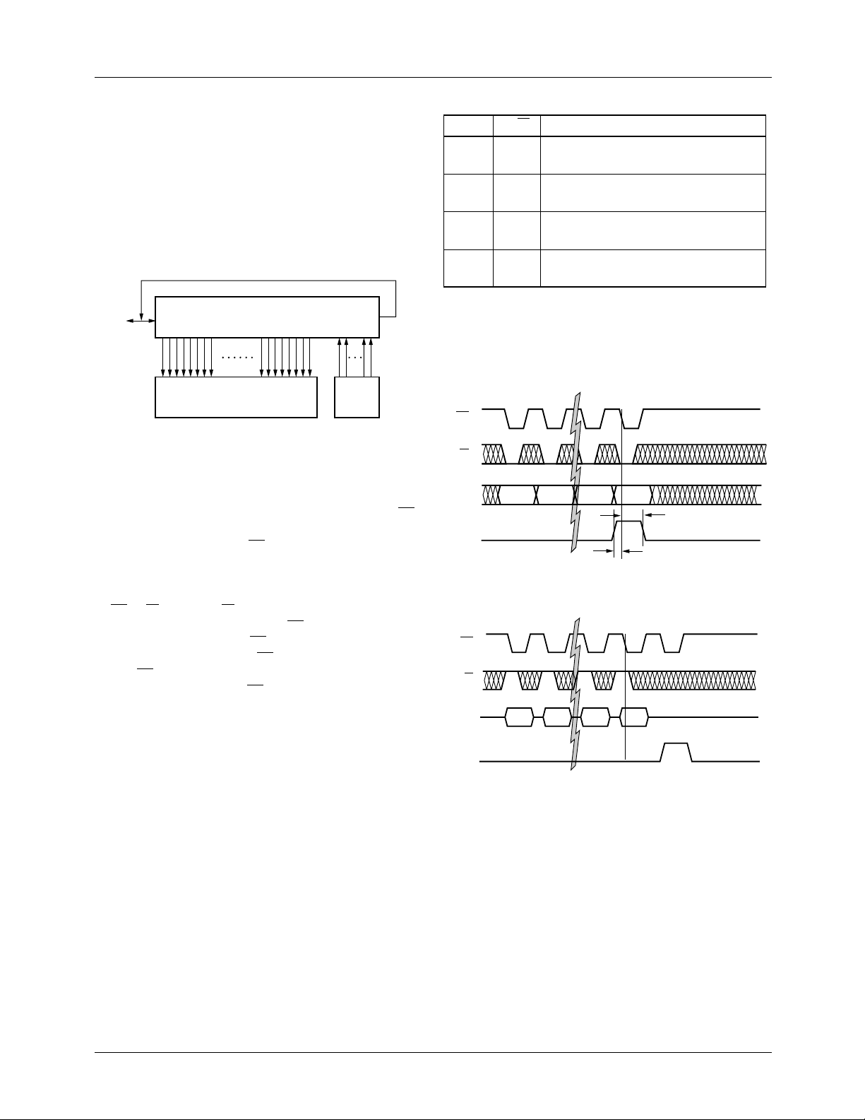
Block Diagram
V
IN1
V
IN2
V
IN3
MUX
CONTROL
0
D
RESET
MICROPROCESSOR
INTERFACE
ANALOG
CLAMP
0
A
CS
R/W
INT
BACK PORCH
CLAMP
GAIN
D/A
D/A
+1.2V
REF
V
COMP
ANALOG INTERFACE DDS/PIXEL CLOCK INTERFACE
A/D
R
LOWPASS
FILTER
DIRECT
DIGITAL
SYNTHESIZER
T
B
R
CLK IN
CLK
OUT
DDS
OUT
DATA
SELECTOR
SUBCARRIER
PHASE-LOCKED
LOOP
SYNC
SEPARATOR
HORIZONTAL
PHASE-LOCKED
LOOP
BYP
C
PFD IN
PXCK SEL
65-22071-01
EXT PXCK
CVBS
7-0
GVSYNC
GHSYNC
PXCK
LDV
VALID
Rev. 1.0.5
Page 2

TMC22071A PRODUCT SPECIFICATION
Functional Description
The TMC22071A is a fully-integrated genlocking video A/D
converter which digitizes NTSC or PAL baseband composite
video under program control. It accepts video on three
selectable input channels, adjusts gain, clamps to the back
porch, and digitizes the video at a multiple of the horizontal
line frequency. It extracts horizontal and vertical sync, measures the subcarrier frequency and phase (relative to the sampling clock), and provides the data along with digital
composite video data over an 8-bit digital video port. Two
sync outputs (GHSYNC
generates 1x (LDV) and 2x (PXCK) pixel clocks for data
transfer. PXCK also serves as a master clock for the companion TMC22x9x Encoders and TMC22x5y decoders.
Operating parameters are set up via a serial microprocessor
port. Internal or external voltage reference operation is available
Timing
The TMC22071A operates from an internally-synthesized
clock, PXCK, which runs at twice the pixel data rate. The
nominal pixel rates may be set to 12.27 Mpps for NTSC and
13.5 Mpps for NTSC and P AL. Customers requiring 14.75 or
15 Mpps PAL operation should consult factory.
Video Input
Three high-impedance video inputs are selected by an internal multiplexer under host processor control. The device
accepts industry-standard video levels of 1.23 Volts (sync tip
to peak color = 1 volt sync tip to reference white). Good
channel-to-channel isolation allows active video on all three
inputs simultaneously. Antialiasing filtering (if used) and
line termination resistors must be provided externally. The
input selection is controlled by two bits in the Control Register.
Analog Clamp
The front-end analog clamp ensures that the input video falls
within the active range of the A/D converter. The digitized
composite video output can be clamped to the back porch by
a secondary digital clamp.
Automatic Gain Adjustment
Since video signals may vary substantially from nominal levels, the TMC22071A performs an automatic level setting
routine to establish correct signal amplitudes for digitizing.
The TMC22071A relies upon the presence of the sync
tip-to-back porch voltage to determine the gain required for
the input video signal.
Sync tip compression or clipping is often affected by APL
(Average Picture Level) variation. Rather than tracking
minor variations in sync tip amplitude and constantly adjusting video gain, the TMC22071A establishes proper signal
and GVSYNC) are also provided. It
amplitudes during initial genlock acquisition, and then
(optionally) holds the gain constant. This results in a stable
picture under variable signal conditions.
Improperly terminated or weak video signals are handled in
the TMC22071A by a selectable gain of +1.0 or +1.5. The
higher gain can amplify a doubly-terminated signal which is
reduced in amplitude by 2/3.
If the input signal levels are well controlled, the automatic
gain adjustment can be disabled and the gain held at its nominal value (unity or 1.5X).
Analog-to-Digital Converter
The TMC22071A contains a high-performance 8-bit A/D
converter. Its gain and offset are automatically set as a part of
the automatic gain adjustment process during initial signal
acquisition, and require no user attention.
The reference voltages to the A/D converter are set up by
internal D/A converters under automatic control during genlock acquisition. These voltages determine the gain and offset of the A/D converter with respect to the video level
presented at its input.
Low-Pass Filter
The digitized composite video stream is digitally low-pass
filtered to remove chrominance components from the sync
separator. Filtering provides robust operation by optimizing
the signal-to-noise ratio of the synchronizing/blanking portion of the video, improving the accuracy of the back porch
blanking level detector.
A digital sync separator provides the output sync signals,
GHSYNC and GVSYNC, and times internal operations.
Horizontal Phase-Locked Loop
A phase-locked loop generates PXCK, at twice the pixel
rate. The reference signal for the horizontal phase-locked
loop is generated by the Direct Digital Synthesizer (DDS).
The DDS output is constructed with an internal D/A converter and is output from the TMC22071A via the DDS OUT
pin. This signal is passed through an external LC filter and
input to the horizontal phase-comparator.
The frequency of the DDS output is one ninth of that of
PXCK.
A 20 MHz clock is required to drive the DDS. Preferably,
this may be input to the TMC22071A via CMOS levels on
the CLK IN pin. Alternately, a 20 MHz crystal may be
directly connected between CLK IN and CLK OUT with
tuning capacitors to activate the internal crystal oscillator circuitry.
If incoming video is lost or disconnected after the
TMC22071A has acquired and locked, PXCK, GHSYNC,
2
Page 3
PRODUCT SPECIFICATION TMC22071A
GVSYNC and GRS data will continue. The GRS data will
be the initial subcarrier frequency and phase values selected
by the Format select bits of the Control Register. The
TMC22071A will acquire and lock to incoming video within
two frames after video is restored.
Subcarrier Phase-Locked Loop
A fully-digital phase-locked loop is used to extract the phase
and frequency of the incoming color burst. These frequency
and phase values are output over the CVBS bus during the
horizontal sync period. Fairchild’s video decoder and genlockable encoder chips will accept these data directly.
Back Porch Digital Clamp
A digital back-porch clamp is employed to ensure a constant
blanking level. It digitally offsets the data from the A/D converter to set the back porch level to precisely 3Ch for NTSC
and 40h for PAL. When the digital clamp is enabled, the
CVBS video output data is determined from the A/D conversion result minus the back porch level + 3Ch (40h for PAL).
Digitized Video Output
The digitized 8-bit video output is provided over an 8-bit
wide CVBS data port, synchronous with PXCK and LDV.
Subcarrier frequency, subcarrier phase, and Field ID data
(GRS) are transmitted in 4-bit nibbles over CVBS
3-0
during
the horizontal sync tip period at the PXCK rate.
Microprocessor Interface
Since microprocessor buses are notoriously noisy from a
wide-band analog point of view, the microprocessor interface bus is only one bit wide, rather than the more customary
eight. The operation of this bus is similar to other buscontrolled devices except that the TMC22071A internal
Control Register is accessed one bit at a time.
A sequence of 47 bits is written to or read from the LSB of a
standard microprocessor port. Writing to or reading from the
secondary address results in the transfer of data to or from
the internal shift register.
The RESET
machines to their initialized conditions. Returning the
RESET pin HIGH starts the signal acquisition sequence
which lasts until locking with the gain-adjusted and clamped
video signal is achieved.
input, when LOW, sets all internal state
Pin Assignments
1
68
65-22071-02
Pin Name Pin Name
V
1
2
3
4
5
6
7
8
9
10
11
12
13
14
15
16
17
DD
CVBS
0
CVBS
1
CVBS
2
CVBS
3
CVBS
4
V
DD
D
GND
CVBS
5
CVBS
6
CVBS
7
GHSYNC
GVSYNC
VALID
D
GND
D
GND
LDV
V
18
DD
PXCK
19
D
20
GND
D
21
GND
V
22
DD
V
23
DDA
A
24
GND
V
25
DDA
V
26
DDA
A
27
GND
R
28
B
V
29
IN3
V
30
DDA
V
31
IN2
A
32
GND
V
33
DDA
V
34
IN1
Pin Name Pin Name
A
35
36
37
38
39
40
41
42
43
44
45
46
47
48
49
50
51
GND
R
T
A
GND
V
REF
A
GND
V
DDA
A
GND
C
BYP
PFD IN
A
GND
DDS OUT
PXCK SEL
V
DDA
COMP
A
GND
D
GND
CLK IN
52
53
54
55
56
57
58
59
60
61
62
63
64
65
66
67
68
V
DD
CLK OUT
EXT PXCK
D
GND
D
GND
D
GND
V
DD
V
DD
A
0
R/W
CS
V
DD
RESET
D
GND
D
0
INT
D
GND
3
Page 4
TMC22071A PRODUCT SPECIFICATION
Pin Assignments (continued)
5180
81
100
130
Notes:
1. NC = Do Not Connect.
* These pins are not connected in the
TMC22071A. However, you should
connect these pins as shown for
compatibility with future genlock ICs.
Pin Name Pin Name
A
1
0
NC
2
50
31
3
4
5
6
7
8
9
10
11
12
13
14
15
16*
17
18
19
20
21
22
23
24
25
NC
R/W
CS
V
DD
RESET
D
GND
D
0
NC
NC
NC
NC
NC
NC
D
GND
INT
V
DD
NC
NC
CVBS
CVBS
CVBS
CVBS
CVBS
Pin Name Pin Name
V
26
DD
D
27
GND
CVBS
28
29
30
31
32
33
34
35
36
37
38
39
40
41*
42*
43
44
45
46
0
47
1
48
2
49
3
50
4
5
CVBS
6
CVBS
7
NC
GHSYNC
GVSYNC
VALID
NC
NC
NC
D
GND
D
GND
LDV
D
GND
V
DD
NC
V
DD
PXCK
D
GND
D
GND
V
DD
V
DDA
A
GND
V
51
DDA
V
52
DDA
NC
53
NC
54
A
55
GND
NC
56
R
57
B
V
58
IN3
NC
59
V
60
DDA
V
61
IN2
NC
62
A
63
GND
V
64
DDA
V
65
IN1
NC
66
A
67
GND
R
68
T
A
69
GND
V
70
REF
NC
71
A
72
GND
V
73
DDA
A
74
GND
C
75
BYP
76
77
78
79
80
81
82
83
84
85
86
87
88
89
90
91
92
93
94
95
96
97
98
99
100
NC
PFD IN
NC
NC
NC
A
GND
DDS OUT
NC
NC
NC
PXCK SEL
V
DDA
COMP
A
GND
D
GND
CLK IN
V
DD
CLK OUT
EXT PXCK
D
GND
D
GND
D
GND
V
DD
NC
V
DD
65-22071-02B
Pin Definitions
Pin Number
68 pin
Pin Name
PLCC
Video Input
V
IN1-3
34, 31, 2965, 61, 581.23Vp-p Composite Video Input. Video inputs,1.25 Volts peak-to-peak, sync
Clocks
CLK IN 51 91 CMOS 20 MHz DDS clock input. 20 MHz CMOS clock input to DDS. This
OUT 53 93 CMOS Inverted clock output. Inverted DDS clock output. This pin may also
CLK
PXCK 19 45 CMOS 2x Pixel clock output. 2x oversampled line-locked clock output.
LDV 17 40 CMOS Pixel clock output. Delayed pixel clock output. LDV runs at 1/2 the
EXT PXCK 54 94 CMOS External PXCK input. Input for external PXCK clock source.
PXCK SEL 46 86 CMOS PXCK source select. Select input for internal or external PXCK.
100 pin
MQFP
Pin Type Function
tip to peak color
pin may also be used along with CLK OUT for directly connecting
crystals.
be used along with CLK IN for directly connecting a crystal.
rate of PXCK and its rising edge is useful for transferring CVBS
digital video from the TMC22071A to the TMC22x9x Digital Video
Encoders.
When HIGH, the internally generated line-locked PXCK is selected.
When LOW, the external PXCK source is enabled.
4
Page 5
TMC22071A PRODUCT SPECIFICATION
Pin Definitions (continued)
Pin Number
68 pin
Pin Name
PLCC
Digital Video
GHSYNC 12 32 CMOS Horizontal sync output. When the TMC22071A is locked to
GVSYNC
CVBS
11-9, 6-230-28,
7-0
mP l/O
D
0
A
0
CS 62 5 TTL Chip select. When CS is HIGH, D0 is in a high-impedance state and
RESET 64 7 TTL Master reset input. Bringing RESET LOW forces the internal state
R/W 61 4 TTL Bus read/write control. When R/W and A0 are LOW, the
INT 67 17 TTL Interrupt output. This output is LOW if the internal horizontal phase
VALID 14 34 TTL HSYNC locked flag. This output, when HIGH indicates that
100 pin
MQFP
Pin Type Function
incoming video, the GHSYNC pin provides a negative-going pulse
after the falling edge of the horizontal sync pulse. There is a fixed
number of PXCK clock cycles between adjacent falling edges of
GHSYNC, except following a VCR headswitch.
13 33 CMOS Vertical sync output. When the TMC22071A is locked to incoming
video, the GVSYNC pin provides a negative-going edge after the
start of the first vertical sync pulse of a vertical blanking interval.
CMOS Composite output bus. 8-bit composite video data is output on this
25-21
bus at 1/2 the PXCK rate. During horizontal sync, field ID, subcarrier
frequency, and subcarrier phase are available on this bus.
66 9 TTL Data l/O port. Microprocessor data port. All control parameters are
loaded into and read back from the Control Register over this 1-bit
bus.
60 1 TTL mP port control. Microprocessor address bus. A LOW on this input
loads the l/O Port Shift Register with data from D0 and CS. A HIGH
transfers the l/O Port Shift Register contents into the Control Register
on the last falling edge of CS.
ignored. When CS is LOW, the microprocessor can read or write D0
data into the Control Register.
machines to their starting states, loads the Control Register with
default values, and disables outputs. Bringing RESET HIGH restarts
the TMC22071A in its default mode.
microprocessor can write to the Control Register over D0. When R/W
is HIGH and A0 is LOW, the contents of the Status Register are read
over D0.
lock loop is unlocked with respect to incoming video for 128 or more
lines per field. After lock is established, INT goes HIGH.
incoming horizontal sync has been detected within the ±16 pixel
window in time established by previous sync pulses. When LOW, it
indicates that incoming horizontal sync has not been found within the
expected time frame. VALID will toggle if the time stability of
incoming video is such that sync positioning varies more than
±16 pixels or if occasional horizontal sync pulses are missing.
5
Page 6
PRODUCT SPECIFICATION TMC22071A
Pin Definitions (continued)
Pin Number
68 pin
Pin Name
Analog Interface
V
REF
COMP 48 88 0.1 mF Compensation capacitor. Compensation for DDS D/A converter
RT,R
B
PLL Filter
DDS OUT 45 82 Internal DDS output. Analog output from the internal Direct Digital
PFD IN 43 77 Horizontal PLL input. Analog input to the Phase/Frequency
C
BYP
Power Supply
V
DDA
V
DD
Ground
A
GND
D
GND
PLCC
36, 28 68 0.1 mF A/D V
23, 25,
26, 30,
33, 40,
1, 7,18,
22, 52,
58,59,63
24, 27,
32, 35,
37, 39,
41, 44,
49,
8, 15,
16, 20,
21, 50,
55-57,
65, 68
100 pin
MQFP
38 70 +1.23 V V
42 75 1 mF Comparator bypass. Decoupling point for the internal comparator
49, 51,
52, 60,
64, 73,
47
87
6, 18,
26, 42,
44, 48,
92, 98,
100
50, 55,
63, 67,
69, 72,
74, 81,
89
8, 16,
27, 38,
39, 41,
46, 47,
90, 95-
97
Pin Type Function
input/output. +1.23 Volt reference. When the internal voltage
REF
reference is used, this pin should be decoupled to A
mF capacitor. An external +1.2 Volt reference may be connected
here, overriding the internal reference source.
circuitry. This pin should be decoupled to V
capacitor.
decoupling. Decoupling points for A/D converter voltage
REF
references. These pins should be decoupled to A
capacitor.
Synthesizer D/A converter, at 1/9 the PXCK frequency.
Detector of the horizontal phase-locked loop.
reference of the Phase/Frequency Detector. This pin should be
decoupled to A
+5 V Analog power supply. Positive power supply to analog section.
+5 V Digital power supply. Positive power supply to digital section.
0.0 V Analog ground. Ground for analog section.
0.0 V Digital ground. Ground for digital section.
with a 0.1 mF capacitor.
GND
with a 0.1 mF
DDA
GND
with a 0.1
GND
with a 0.1 mF
6
Page 7
PRODUCT SPECIFICATION TMC22071A
Control and Status Registers
The TMC22071A is controlled by a single 47-bit long Control Register. Access to the Control Register is via the I/O
Port Shift Register arranged as shown in Figure 1. The Control Register can be written, with the desired programming.
The 12-bit Status Register is read-only and accessed through
the same l/O Port Shift Register. Reading the Status Re gister
yields information about blanking level, subcarrier presence,
and whether or not PXCK is locked or unlocked with respect
to the line rate.
D
0
0464758
Figure 1. Control and Shift Register Structure
The host processor writes data into the TMC22071A using
only one bit of the microprocessor’s data and address b us. As
shown in Figure 2, the user should bring A0 high for the CS
falling edge preceding the introduction of bit 0 to the D0
port. The next rising edge of CS completes the preloading of
the control data, which transfer into the control register on
the next rising edge of the pixel clock. The I/O Port Shift
Register, Control Register and Status Register are governed
by CS, R/W, and A0. R/W and A0 are latched by the
TMC22071A on the falling edge of CS and data input D0 is
latched on the rising edge of CS. Data read from D0 is
enabled by the falling edge of CS and disabled by the rising
edge of CS
. When the Control Register is read more than
once consecutively, an extra CS pulse and accompanying A0
is needed to align the circulated shift register data.
I/O Port Shift Register
Control Register
Status
Register
65-22071-03
Table 1. Microprocessor Port Control
A
The full sequence of 47 bits of Control Register data must be
written each time a change in that data is desired. All or a
few of the Control and Status Register bits may be read,
but the sequence always begins with bit 58 of the Status
Register.
CS
R/W
D
A
CS
R/W
R/W Action
0
0 0 Write data from D0 into l/O Port Shift
Register
0 1 Read D0 data from last stage of l/O
Port Shift Register
1 0 Transfer l/O Port Shift Register
contents to Control Register
1 1 Enables continuous update of status
bits in l/O Port Shift Register
0
0
D
46 45 1 0
Figure 2. Data Write Sequence
0
58 57 1 0
t
H
t
S
65-22071-04
A
0
65-22071A-05
Figure 3. Data Read Sequence
7
Page 8
TMC22071A PRODUCT SPECIFICATION
0
SRESET
FORMAT
24 31 32 39 40 46
AGC
LEADLAG
7 8 15 16 23
00
000
VGAIN
TEST
000 00000 001
TEST
FREERUN
TEST
SOURCE
TEST
VCR/TV
BPFOUT
CVBSEN
STATUS REGISTER
47 54
(LSB)
COLOR
SUBPIX
DCLAMP
BLKAMP
TEST
55 58
(MSB)
(LSB)
LOCK
STVAL
TEST
TEST
LEADLAG
TEST
65-22071-06
TEST
GRSONLY
Figure 4. Control Register Map
Control Register Bit Functions
Bit Name Function
0 SRESET Software reset. When LOW, resets and holds internal state machines, resets Control
Register with previously written values, and disables output drivers. When HIGH,
SRESET starts and runs state machines, PXCK, and enables outputs.
1-3 FORMAT Input signal format select.
Bit 3 is the MSB.
000 NTSC at 12.27 Mpps.
001 NTSC at 13.5 Mpps.
010 Reserved.
011 Reserved.
100 PAL at 13.5 Mpps.
101 Reserved.
11x Reserved.
4-6 TEST Factory test control bits. These should be set LOW.
7,8 SOURCE Video source select. Bit 8 is the MSB.
00 V
IN1
01 V
IN2
1x V
IN3
9 VGAIN Video gain. When LOW, gain is set to unity. When HIGH, gain is set to 1.5X.
10-11 TEST Factory test control bits. These should be set LOW.
12-16 SUBPIX These control bits allows the HSYNC, VSYNC, and sample clock to be time-shifted by
-16/32 to +15/32 pixels. Bit 16 is the two’s complement MSB. When SUBPIX is 00h,
HSYNC and incoming video are subject to LEADLAG. A value of 18h delays HSYNC
1/4 pixel. A value of 08
17-24 LEADLAG This control word allows the HSYNC and VSYNC to be time-shifted -122 to +132 LDV
cycles. When LEADLAG is 7B
83h delays HSYNC eight LDV cycles. A value of 73h advances HSYNC eight LDV
cycles. Bit 24 is the MSB.
advances HSYNC 1/4 pixel.
h
, HSYNC and incoming video are in alignment. A value of
h
8
Page 9

PRODUCT SPECIFICATION TMC22071A
Control Register Bit Functions (continued)
Bit Name Function
25 AGC AGC operation control. After H and V sync acquisition, the A/D converter references are
adjusted to encompass the full video range. The system can initiate an A/D adjustment
sequence at any time by bringing this bit HIGH. The control bit will reset to 0 following
AGC adjustment.
26 FRERUN When HIGH, a free-running PXCK is generated, independent of incoming video. When
LOW, PXCK is locked to incoming video.
27-29 TEST Factory test control bits. These should be set LOW.
30 VCR/TV Block sync enable. When HIGH the TMC22071A accepts both normal and block sync.
(In block sync, the incoming signal is at the sync tip level for 2.5 (PAL) or 3 (NTSC)
consecutive lines. Equalization pulses may be absent.) When LOW, only normal sync
may be input. For most applications, whether using a VCR or a studio video input
source, best performance will be found when this bit is HIGH.
31 CVBSEN CVBS bus enable. When LOW, the CVBS
high-impedance state. When HIGH, they are enabled.
32 TEST Factory test control bit. This should be set LOW.
33 BPFOUT Burst phase / frequency output control. When HIGH, GRS is disabled. When LOW, burst
phase and frequency information is output on CVBS
34 DCLAMP Digital clamp enable. The digital clamp is enabled when DCLAMP is HIGH and disabled
when LOW.
35-39 TEST Factory test control bits. These should be set LOW.
40-43 STVAL Sync tip value. When DCLAMP is HIGH and STVAL is set to its default value 3h the
output sync level is 3h for NTSC and 7h for PAL. Bit 43 is the MSB.
44 VCR VCR lock control. Setting this bit LOW improves the TMC22071A’s locking to VCR
signals. When only clean video input signals are used, the user may set this bit HIGH for
compatibility with existing TMC22071 firmware.
45 TEST Factory test control bit. This should be set LOW.
46 GRSONLY When the horizontal phase lock loop becomes unlocked (i.e. after video input is
disconnected) and this Control Bit is HIGH, all CVBS data is forced LOW except
subcarrier frequency and phase data (GRS). GHSYNC, GVSYNC, and PXCK continue
with default GRS data until video is required. The presence of GRS also depends upon
bit 33. If the GRSONLY bit is LOW, GHSYNC, GVSYNC, and PXCK continue with
default GRS data continue but video pixel data is random.
Status Bits (Read Only)
47 COLOR Burst present status bit. This bit is HIGH when burst is present on the input video. It is
LOW, when burst is not present.
48-55 BLKAMP Blanking amplitude status bit. These eight bits report the actual blanking level.
56 LOCK H-lock loop status bit. When HIGH, the TMC22071A is not locked to an input signal.
When LOW, lock has been achieved.
57-58 TEST These are read-only bits for testing puposes only.
, GHSYNC, and GVSYNC outputs are in a
7-0
.
3-0
9
Page 10

TMC22071A PRODUCT SPECIFICATION
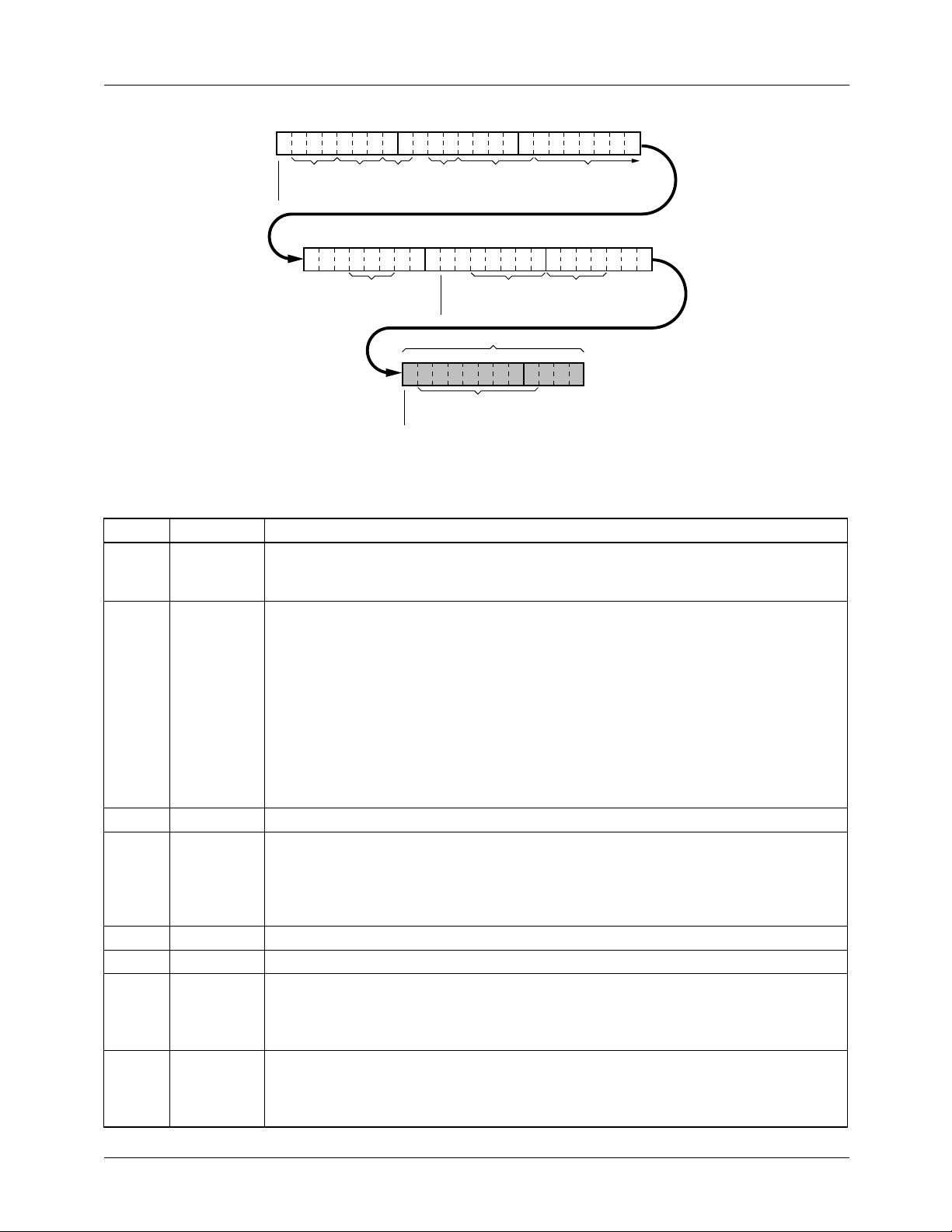
Horizontal Timing
Horizontal line rate is selectable, and is determined by the
FORMAT control bits (12.27 Mpps for NTSC, 13.5 Mpps
for NTSC and PAL). Figure 5 illustrates the horizontal
blanking interval. Figure 6 completes the definition of timing
parameters with vertical blanking interval detail.
Video In
GHSYNC
t
DH
Figure 5. Horizontal Sync Timing
Burst
65-22071-07
H
0.5H
4.7 µsec
Serration
t
VD
65-22071-08
Video In
GVSYNC
GHSYNC
(Odd Field)
GHSYNC
(Even Field)
2.35 µsec PAL
2.3 µsec NTSC
Equalizing Pulse
t
DH
Figure 6. Vertical Sync timing
Programming the TMC22071A
Upon power-up after bringing RESET LOW, the
TMC22071A Control Register is set to default values as
shown in the top entry of Table 3. These default values do
not necessarily render the TMC22071A operational in any
specific application. Before the TMC22071A is expected to
acquire input video, its Control Register must be loaded with
data that is specific to its use.
Table 2.TMC22071A Timing Options
Field
Standard
Rate (Hz)
NTSC 59.94 15.734264 12.2727+ 24.54+ 780
NTSC-601 59.94 15.734264 13.50 27.0 858
PAL-601 50.00 15.625 13.50 27.0 864
Line
Rate (kHz)
Pixel
Rate (Mpps)
PXCK
Frequency (MHz)
Plxels
Per Line
Table 3. Control Register Example Data
Control Register Data (Bit 56 …… Bit 0)
Standard
DEFAULT 0000 0110 0000 1001 0000 0010 0000 0000 0000 0000 0000 001
NTSC 0010 0110 0000 1001 1000 0010 0000 0000 0000 00xx 0000 000
NTSC-601 0010 0110 0000 1001 1000 0010 0000 0000 0000 00xx 0000 010
PAL-601 0010 1110 0000 1001 1000 0010 0000 0000 0000 00xx 0001 xx0
46 42 38 34 30 26 22 18 14 10 6 2
10
Page 11

PRODUCT SPECIFICATION TMC22071A
9
CVBS Bus Data Formats
The CVBS bus outputs a Genlock Reference Signal (GRS)
along with the 8-bit digital composite video data. The range
of output data versus video input voltage is illustrated in
Figure 7 where sync tip and blanking levels are controlled by
the digital backporch clamp of the TMC22071A. During
horizontal sync, the TMC22071A outputs field identification, subcarrier frequency, and subcarrier phase information
on the CVBS bus.
Peak Chrominance
Peak Luminance
Back Porch
Burst
Sync Tip
Blanking
Figure 7. Output Data vs. Input Video Level
NTSC PAL
FEhFF
D2hCF
3Ch40
03h03
65-22071-0
Field identification is output on CVBS
. The LSB,
2-0
CVBS0, will be LOW during odd fields and HIGH for even
fields. When NTSC operation is selected, CVBS
00,01,10,11 for fields 1 through 4 respectively. When PAL
operation is selected, CVBS
count 000, 001, 010, etc. to
2-0
111 for fields 1 through 8, respectively.
CVBS3 indicates V-component inversion in PAL. It is HIGH
for NTSC lines (burst 135°) and LOW for PAL lines (burst
225°)
h
Subcarrier frequency is sent out in a 24-bit binary represen-
h
tation in six 4-bit nibbles on CVBS
data, f
, is identical to the pre-programmed BSEED value
23-0
. Subcarrier frequency
3-0
used in the TMC22071A to lock the subcarrier phase-locked
loop to the incoming subcarrier frequency.
Subcarrier phase, F
h
representation in six 4-bit nibbles on CVBS
, is also sent out in a 24-bit binary
23-0
3-0
the MSB.
h
count
1-0
. Bit F23 is
PXCK
GHSYNC
CVBS
7:0
01
GHSYNC
CVBS
2 3 57 58 59 60 61 62 63 64 65 66 67 68 69 70 71 72 73 74 75 76
PIXEL PIXEL PIXEL
PXCK
t
DO
LDV
t
HO
7:0
f
23:20f19:16f15:12f11:8f7:4f3:0f23:20f19:16f15:12f11:8f7:4f3:0
FREQUENCY PHASE
FIELD IDENTIFICATION
Figure 8. Genlock Reference Signal (GRS) Format
t
PWHPXtPWHPX
t
XL
PIXEL 0 PIXEL 1
t
XV
1/f
PXCK
Figure 9. CVBS Bus Video Data Format
PIXEL PIXEL
65-22071-10
65-22071-11
11
Page 12

TMC22071A PRODUCT SPECIFICATION
CS
R/W
A
D
CS
R/W
A
D
t
SA
t
PWLCS
t
HA
t
PWHCS
0
t
SD
t
HD
0
65-22071-12
Figure 10. Microprocessor Port – Write Timing
t
PWLCS
t
SA
t
HA
0
t
DOM
0
t
DOZ
t
PWHCS
t
HOM
65-22071-13
Figure 11. Microprocessor Port – Read Timing
12
Page 13

PRODUCT SPECIFICATION TMC22071A
Equivalent Circuits and Transition Levels
V
DD
V
150½
DD
PFD IN
C
BYP
+2.4 V
2k½
+
–
n Substrate
V
DD
V
DD
pp
np
65-22071-14
Figure 12. Equivalent PFD IN Circuit Figure 13. Equivalent DDS OUT Circuit
V
DD
p
Input
n Substrate
V
DD
p
DDS OUT
65-22071-15
Output
n
65-22071-16
n
65-22071-17
Figure 14. Equivalent Digital Input Circuit Figure 15. Equivalent Digital Output Circuit
t
DOM
CS
t
HOM
D
0
0.5 V
Hi-Z
0.5 V
t
DOZ
2.0 V
0.8 V
65-22071-18
Figure 16. Transition Levels for Three-State Measurements
13
Page 14

TMC22071A PRODUCT SPECIFICATION
Absolute Maximum Ratings (beyond which the device may be damaged)
1
Parameter Min. Max. Unit.
Power Supply Voltage -0.5 7.0 V
Input Voltage -0.5 VDD + 0.5 V
Digital Outputs
Applied Voltage
Forced Current
2
3,4
-0.5 VDD + 0.5 V
-6.0 6.0 mA
Short Circuit Duration (single output in HIGH state to GND) 1 sec
Temperature
Operating, Case -60 130 °C
Operating, Junction 150 °C
Lead Soldering (10 seconds) 300 °C
Vapor Phase Soldering (1 minute) 220 °C
Storage -65 150 °C
Notes:
1. Absolute maximum ratings are limiting values applied individually while all other parameters are within specified operating
conditions. Functional operation under any of these conditions is NOT implied.
2. Applied voltage must be current limited to specified range, and measured with respect to GND.
3. Forcing voltage must be limited to specified range.
4. Current is specified as conventional current, flowing into the device.
Operating Conditions (for standard temperature range)
Parameter Min. Nom. Max. Units
V
DD
V
IH
V
IL
IOH Output Current, Logic HIGH -2.0 mA
lOL Output Current, Logic LOW 4.0 mA
V
IN
V
REF
T
A
Microprocessor Interface
t
PWHCS
t
PWHCS
t
SA
t
HA
t
SD
t
HD
Note:
1. Timing reference points are at the 50% level.
Power Supply Voltage 4.75 5.0 5.25 V
Input Voltage, Logic HIGH
TTL Inputs 2.0 V
CMOS Inputs 2/3V
DD
DD
V
DD
Input Voltage, Logic LOW
TTL Inputs D
CMOS Inputs D
GND
GND
0.8 V
1/3 V
DD
Video Input Signal Level, Sync Tip to Peak White 1.0 V
External Reference Voltage 1.235 V
Ambient Temperature, Still Air 0 70 °C
CS Pulse Width, LOW 50 ns
CS Pulse Width, HIGH 50 ns
Address Setup Time 0 ns
Address Hold Time 16 ns
Data Setup Time 20 ns
Data Hold Time 0 ns
V
V
V
14
Page 15

PRODUCT SPECIFICATION TMC22071A
Electrical Characteristics (for standard temperature range)
Parameter Conditions Min Typ Max Units
I
DD
I
REF
Power Supply Current
Reference Inputcurrent V
IIH Input Current, Logic HIGH VDD = Max, VIN = 4.0V ±10 mA
I
IL
V
V
I
OZH
I
OZL
C
C
C
R
Note:
1. Typical I
Input Current, Logic LOW VDD = Max, VIN = 0.4V ±10 mA
Output Voltage, Logic HIGH IOH = -2.0 mA 2.4 V
OH
Output Voltage, Logic LOW IOL = 4.0 mA 0.4 V
OL
Hi-Z Output Leakage current, HIGH VDD = Max, VIN = V
Hi-Z Output Leakage current, LOW VDD = Max, VIN =GND ±10 mA
Digital Input Capacitance TA = 25°C, f = 1 Mhz 4 15 pF
l
Digital Output Capacitance TA - 25°C, f = 1 Mhz 10 pF
O
Input Capacitance, V
V
Input Resistance, V
V
with VDD = +5.0 Volts and TA = 25°C, Maximum IDD with VDD = +5.25 Volts and TA = 0°C.
DD
1
IN1-3
IN1-3
Total Current
190 230 mA
VDD = Max,
f
= 30MHz
PXCK
= +1.235V 100 mA
REF
DD
±10 mA
TA = 25°C, f = 3.58 Mhz 15 pF
50 kW
Switching Characteristics (for standard temperature range)
Parameter Conditlons Min Typ Max Units
t
DO
t
HO
f
PCK
f
PXCK
t
PWHPX
t
PWHPX
t
DH
t
VD
t
XL
t
XV
t
DOM
t
HOM
t
DOZ
Output Delay Time C
= 35 pF 2 15 ns
LOAD
Output Hold Time 3 8 ns
Pixel Rate 12 15.3 MHz
Master Clock Rate 24 30.6 MHz
PXCK Pulse Width, LOW 12 ns
PXCK Pulse Width, HIGH 12 ns
Horizontal Sync to GHSYNC 14 pixels
Vertical Sync to GVSYNC 14 pixels
PXCK LOW to LDV HIGH 8 ns
PXCK LOW to LDV LOW 8 ns
D0 enable time 20 ns
D0 disable time 10 15 ns
CS LOW to D0 output driven 5 ns
15
Page 16

TMC22071A PRODUCT SPECIFICATION
System Performance Characterlstics
Parameter Min Type Max Units
E
E
t
V
AL
SCH
SCP
XT
Sync time-base variation
Subcarrier Phase Error
Line-lock Acquisition Time 2 frames
Channel-to-Channel Crosstalk @3.58 Mhz -35 dB
Note:
1. NTSC/PAL compliant black burst at nominal input level ±10%, frequencies nominal ±10 ppm.
Digital Supply Plane
75½
75½
75½
3.3 µF
3.3 µF
3.3 µF
Video A
Video B
Video C
LPF
LPF
LPF
20 MHz, TTL
1
1
+5V
10µF
0.1µF 0.1µF
D
VDDV
GND
V
IN1
V
IN2
V
IN3
EXT PXCK
CLK IN
CLK OUT
PXCK SEL
Ferrite Bead
Analog Supply Plane*
10µF
DDAAGND
TMC22071A
Genlocking
Video Digitizer
INT
VALID
RESET
D0A0CS
DDS OUT
R/W
6.8 pF
10µH
150 pF
C
BYP
0.1µF
390
pF
PFD IN
CVBS
GHSYNC
GVSYNC
0.01 µF
COMP
V
REF
R
T
R
B
7:0
PXCK
LDV
±3ns
±2 degrees
+5V
0.1µF
3.3K½
LM385-1.2
0.1µF
0.1µF
8
0.1µF
DIGITAL VIDEO
INTERFACE
and must be connected
via low-impedance path
Figure 17. Typical Interface Circuit
Application Notes
The TMC22071A is a complex mixed-signal VLSI circuit.
It produces CMOS digital signals at clock rates of up to 15
MHz while processing analog video inputs with a resolution of less than a few millivolts. To maximize performance
it is important to provide an electrically quiet operating
environment. The circuit shown in Figure 17 provides an
optional external 1.2V reference to the V
TMC22071A. The internal V
source is adequate for
REF
most applications.
Flltering
Inexpensive low-pass anti-aliasing filters are shown in Figures 18 and 20. These filters would normally be inserted in
the video signal path just before the 75W terminating resistor and AC-coupling capacitor for each of the three video
inputs, V
. The filter of Figure 18 exhibits a 5th-order
IN1-3
input of the
REF
MICROPROCESSOR
INTERFACE
*section of supply plane beneath
analog interface circuitry
65-22071A-19
Chebyshev response with-3dB bandwidth of 6.7MHz and a
group delay of 140 nanoseconds at 5MHz. The filter of Figure
19 has been equalized for group delay in the video signal
band. Its -3dB passband is 5.5MHz while the group delay is
constant at 220 nanoseconds through the DC to 5MHz
frequency band.
2.2µH
470 pF
Figure 18. Simple Anti-aliasing Filter
2.2µH
470 pF1000 pF
65-22071-20
16
Page 17

PRODUCT SPECIFICATION TMC22071A
430 pF
3.3 µH 3.3 µH 4.7 µH
750 pF 430 pF
Figure 19. Group Delay Equalizer Filter
470 pF 470 pF
2.2 µH
4.7 µH
910 µH
65-22071-21
Using a 20 MHz Crystal
In systems where a 20 MHz clock is not available, a crystal
may be used to generate the clock to the TMC22071A. The
crystal must be a 20 MHz “fundamental” type, not overtone.
Specific crystal characteristics are listed in Table 4 and the
connections are shown in Figure 20.
Table 4. Crystal Parameters
Parameter Value
Fundamental frequency 20 MHz
Tolerance ±30 ppm @ 25°C
Stability ±50 ppm, 0°C to 70°C
Load Capacitance 20 pF
Shunt Capacitance 7 pF Max.
ESR 50 W, Max.
33 pF
20 MHz
Crystal
33 pF
Figure 20. Direct Crystal Connections
TMC22071A
CLK IN
1M½
300½
CLK OUT
65-22071A-22
Grounding
The TMC22071A has separate analog and digital circuits. To
minimize digital crosstalk into the analog signals, the power
supplies and ground connections are provided over separate
pins (VDD and V
pins; D
GND
and A
are digital and analog power supply
DDA
are digital and analog ground pins).
GND
In general, the best results are obtained by tying all grounds
to a solid, low-impedance ground plane. Power supply pins
should be individually decoupled at the pin. Power supply
noise isolation should be provided between analog and digital supplies via a ferrite bead inductor on the analog lead.
Ultimately all +5 Volt power to the TMC22071A should
come from the same power source.
Another approach calls for separating analog and digital
ground. While some systems may benefit from this strategy,
analog and digital grounds must be kept within 0.1V of each
other at all times.
Interface to the TMC22x9x Encoder
The TMC22x9x Digital Video Encoders have been designed
to directly interface to the TMC22071A Digital Video
Genlock. The TMC22071A is the source for TMC22x9x
input signals CVBS
PXCK as shown in Figure 21. These signals directly connect
to the TMC22x9x. The microprocessor interface for
TMC22x9x and TMC22071A are identical. All R/W,
RESET, data and address bus signals from the host microprocessor are shared by the TMC22x9x and TMC22071A.
Only CS, VALID, and INT signals are separate from the
microprocessor bus.
, GHSYNC, GVSYNC, LDV, and
7-0
GENLOCKING VIDEO DIGITIZER
TMC22071A
RESET
D0A0CS
R/W
Figure 21. TMC22x9x Interface Circuit
CVBS
7:0
GHSYNC
GVSYNC
PXCK
LDV
MICROPROCESSOR INTERFACE
8
CVBS
GHSYNC
GVSYNC
PXCK
LDV
2
7:0
TMC22x9x
DIGITAL VIDEO ENCODER
7:0
RESET
D
8
1:0
A
CS
R/W
65-22071A-23
17
Page 18

TMC22071A PRODUCT SPECIFICATION
Printed Circuit Board Layout
Designing with high-performance mixed-signal circuits
demands printed circuits with ground planes. Wire-wrap is
not an option. Overall system performance is strongly influenced by the board layout. Capacitive coupling from digital
to analog circuits may result in poor picture quality. Consider the following suggestions when doing the layout:
1. Keep the critical analog traces (COMP,V
DDS OUT, PFD IN, C
BYP
, and V
IN1-3
sible and as far as possible from all digital signals. The
TMC22071A should be located near the board edge,
close to the analog output connectors.
2. The digital power plane for the TMC22071A should be
that which supplies the rest of the digital circuitry. A single power plane should be used for all of the V
If the analog power supply for the TMC22071A is the
same as that of the system’s digital circuitry, power to
the TMC22071A V
pins should be decoupled with
DDA
ferrite beads and 0.1 mF capacitors to reduce noise.
3. The ground plane should be solid, nor cross-hatched.
Connections to the ground plane should have very short
leads.
, RT, RB,
REF
) as short as pos-
pins.
DD
4. Decoupling capacitors should be applied liberally to
V
pins. Remember that not all power supply pins are
DD
created equal. They typically supply adjacent circuits on
the device, which generate varying amounts of noise.
For best results, use 0.1mF capacitors in parallel with
10mF capacitors. Lead lengths should be minimized.
Ceramic chip capacitors are the best choice.
5. If the digital power supply has a dedicated power plane
layer, it should not overlap the TMC22071A, the voltage
reference or the analog outputs. Capacitive coupling of
digital power supply noise from this layer to the
TMC22071A and its related analog circuitry can
degrade performance.
6. CLK should be handled carefully. Jitter and noise on
this clock or its ground reference may degrade performance. Terminate the clock line carefully to eliminate
overshoot and ringing.
Related Products
• TMC22x9x Digital Video Encoders
• TMC2242/TMC2243/TMC2246 Video Filters
• TMC2081 Digital Video Mixer
• TMC22x5y Digital Decoders
• TMC2302 Image Manipulation Sequencer
18
Page 19

PRODUCT SPECIFICATION TMC22071A
Notes:
19
Page 20

TMC22071A PRODUCT SPECIFICATION
Notes:
20
Page 21

PRODUCT SPECIFICATION TMC22071A
Notes:
21
Page 22

TMC22071A PRODUCT SPECIFICATION
Mechanical Dimensions
68 Lead PLCC Package
Symbol
A .165 .200 4.19 5.08
A1 .090 .130 2.29 3.30
A2 .020 .51
B .013 .021 .33 .53
B1 .026 .032 .66 .81
D/E .985 .995 25.02 25.27
D1/E1 .950 .958 24.13 24.33
D3/E3 .800 BSC 20.32 BSC
e
J .042 .056 1.07 1.42 2
ND/NE 17 17
N
ccc .004 0.10——
Inches
Min. Max. Min. Max.
——
.050 BSC 1.27 BSC
68 68
Millimeters
E
E1
Notes
Notes:
1.
All dimensions and tolerances conform to ANSI Y14.5M-1982
2.
Corner and edge chamfer (J) = 45¡
3.
Dimension D1 and E1 do not include mold protrusion. Allowable
protrusion is .101" (.25mm)
3
J
D D1
D3/E3
e
A
A1
A2
B
B1
J
-C-
LEAD COPLANARITY
ccc C
22
Page 23

PRODUCT SPECIFICATION TMC22071A
Mechanical Dimensions (continued)
100 Lead MQFP Package – 3.2mm Footprint
Symbol
A — .134 — 3.40
A1 .010 — .25 —
A2 .100 .120 2.55 3.05
B .008 3, 5
C .005 .13
D .904 .923 22.95 23.45
D1 .783 .791 19.90 20.10
E .667 .687 16.95 17.45
E1 .547 .555 13.90 14.10
e
L .028 .040 .73 1.03
N
ND
NE
a 0¡ 7¡ 0¡ 7¡
ccc
B
e
Inches
Min. Max. Min. Max.
.015 .38
.009 .23
.0256 BSC .65 BSC
100 100
30 30
20 20
— .004 — .12
D
Pin 1 Indentifier
Millimeters
.22
D1
Notes
E1
E
Notes:
1.
All dimensions and tolerances conform to ANSI Y14.5M-1982.
2.
Controlling dimension is millimeters.
3.
Dimension "B" does not include dambar protrusion. Allowable
dambar protrusion shall be .08mm (.003in.) maximum in excess of
the "B" dimension. Dambar cannot be located on the lower radius
or the foot.
4.
5
4
"L" is the length of terminal for soldering to a substrate.
5.
"B" & "C" includes lead finish thickness.
.20 (.008) Min.
0¡ Min.
Datum Plane
.13 (.005) R Min.
0.076" (1.95mm) Ref
Lead Detail
L
.13 (.30)
.005 (.012)
C
R
a
AA2
A1
B
Seating Plane
See Lead Detail
Base Plane
-C-
Lead Coplanarity
ccc C
23
Page 24

TMC22071A PRODUCT SPECIFICATION
Ordering Information
Product Number Temperature Range Screening Package Package Marking
TMC22071AR1C TA = 0°C to 70°C Commercial 68-Lead PLCC 22071AR1C
TMC22071AKHC
Note:
1. 100 Lead MQFP is strongly recommended for all new board designs.
1
TA = 0°C to 70°C Commercial 100-Lead MQFP 22071AKHC
LIFE SUPPORT POLICY
FAIRCHILD’S PRODUCTS ARE NOT AUTHORIZED FOR USE AS CRITICAL COMPONENTS IN LIFE SUPPORT DEVICES
OR SYSTEMS WITHOUT THE EXPRESS WRITTEN APPROVAL OF THE PRESIDENT OF FAIRCHILD SEMICONDUCTOR
CORPORATION. As used herein:
1. Life support devices or systems are devices or systems
which, (a) are intended for surgical implant into the body,
or (b) support or sustain life, and (c) whose failure to
perform when properly used in accordance with
2. A critical component in any component of a life support
device or system whose failure to perform can be
reasonably expected to cause the failure of the life support
device or system, or to affect its safety or effectiveness.
instructions for use provided in the labeling, can be
reasonably expected to result in a significant injury of the
user.
www.fairchildsemi.com
7/24/98 0.0m 002
Ó 1998 Fairchild Semiconductor Corporation
Stock#DS7022071A
 Loading...