

Page 1
www.fairchildsemi.com
REV. 1.0.0 2/4/03
Features
• Very high performance, low cost
• Adaptive comb-based decoding
• Multiple pin-compatible versions
- 3-line, 2-line, and band-split
- 8- and 10-bit processing
• Internal digital linestores
• Supports NTSC/PAL field and NTSC frame based
decoding
• Multiple input formats
- CCIR-601/624 (D1), D2, CVBS, YC
• Multiple output formats
- CCIR-601/624 (D1), RGB, YC
BCR
• 10-18 Mpps data rate
• Parallel and serial control interface
• Single +5V power supply
Applications
• Studio television equipment
• Personal computer video input
• MPEG and JPEG compression inputs
Description
The TMC22x5yA family of Digital Video Decoders offers
unprecedented, broadcast-quality video processing performance in a single chip. It accepts line-locked or subcarrierlocked composite, YC, or D1 digital video and produces digital components in a variety of formats.
An internal three-line adaptive comb decoder structure produces optimal picture quality with a wide range of source
material. NTSC/PAL field and NTSC frame based decoding
is supported with external memory. Full comb programmability allows the user to tailor the decoder’s response to a
particular systems goals.
A family of products offers 3-line, 2-line, and simple decoders in 8-bit and 10-bit versions—all in a pin and softwarecompatible format. Serial and parallel control ports are provided. These submicron CMOS devices are packaged in a
100-lead Metric Quad Flat Pack (MQFP).
Related Products
• TMC22071 Genlocking Video Digitizer
• TMC22x9x 8 bit Digital Video Encoders
• TMC2081 Digital Video Mixer
• TMC3003 Triple 10-bit D/A Converter
• TMC1185 10 bit A/D converter
• TMC2192 10 bit video encoder
• TMC2072 Enhanced Genlocking Video Digitizer
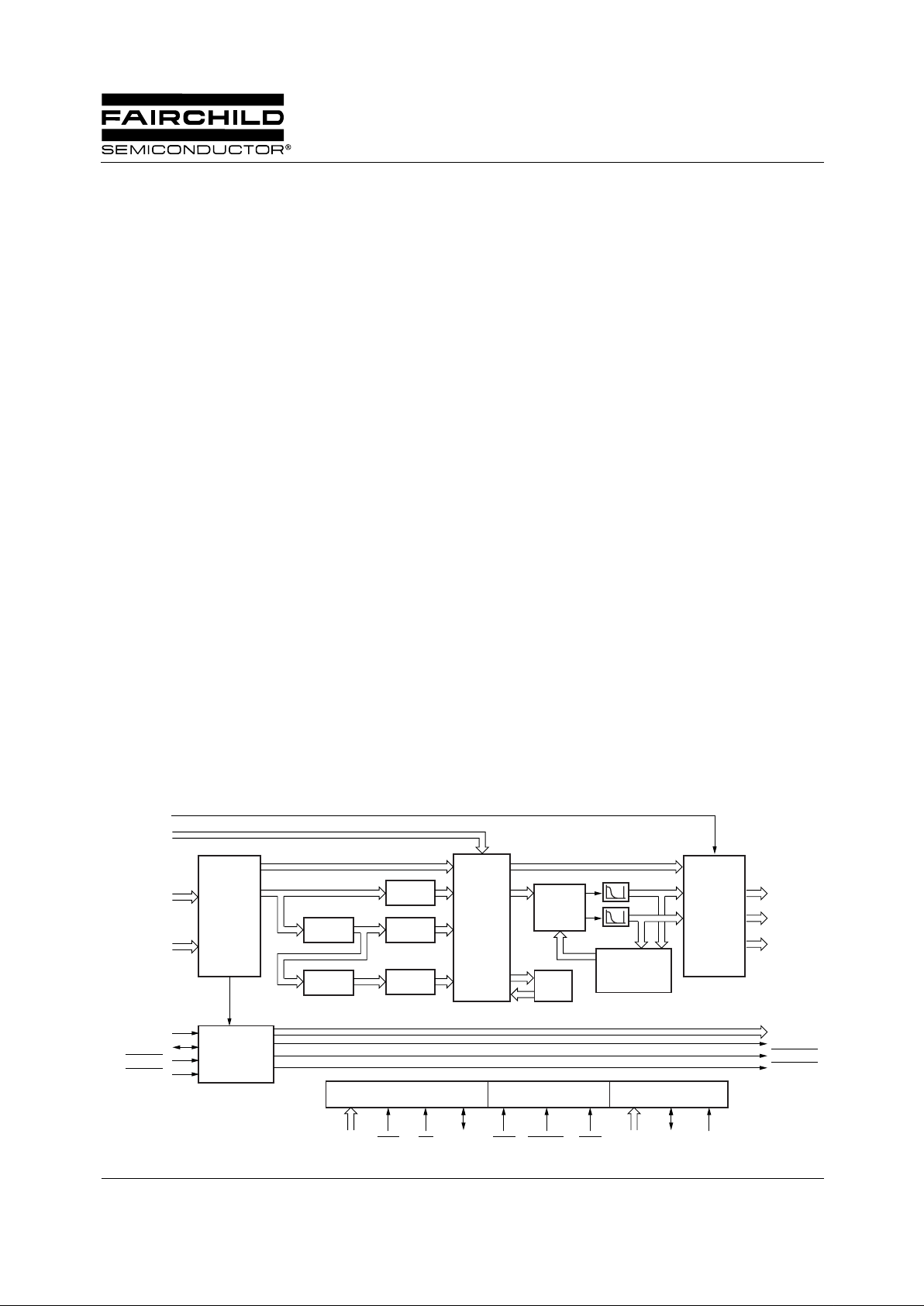
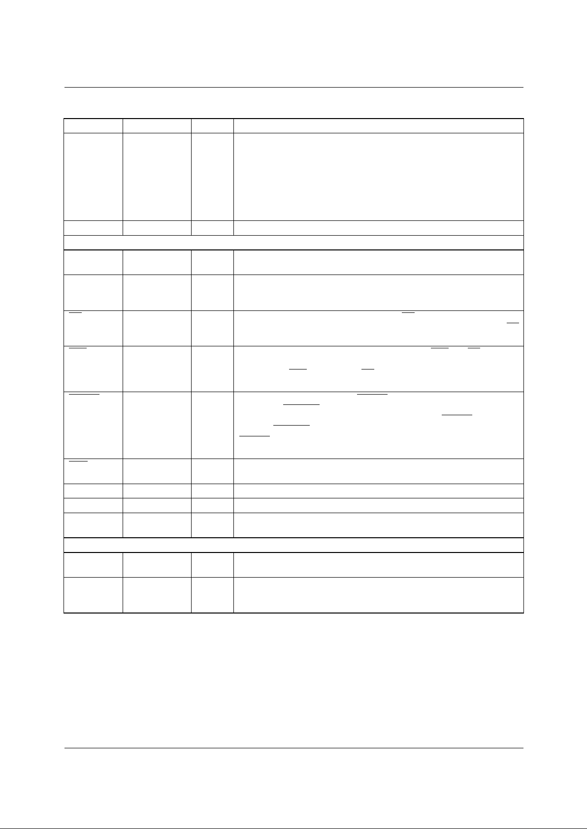
Block Diagram
65-22x5y-01
Input
Processor
Output
Processor
Adaptive
Comb
Filter
VIDEOA
9-0
VIDEOB
9-0
G/Y
9-0
MASTER
1-0
BUFFER
CLOCK
HSYNC
VSYNC
LDV
DHSYNC
DVSYNC
DREF
FID
2-0
B/Cb
9-0
R/Cr
9-0
SER
A
1-0
SA
2-0
RESETSET
R/W SDACS SCL
D
7-0
Parallel Control Serial Control
Global Control
Internal
Sync Pulse
Generator
Y/C Split0
Y/C Split1
Linestore1
Linestore2
Y/C Split2
Chroma
Demod
Comb
Fail
Burst
Locked
Loop
TMC22x5yA
Multistandard Digital Video Decoder
Three-Line Adaptive Comb Decoder Family, 8 & 10 bit
Page 2

TMC22x5yA PRODUCT SPECIFICATION
2 REV. 1.0.0 2/4/03
Table of Contents
Features......................................................................1
Applications ...............................................................1
Description .................................................................1
Block Diagram............................................................1
Contents .....................................................................2
List of Tables and Figures ........................................3
General Description...................................................4
Input Processor...............................................................4
Adaptive Comb Filter.....................................................4
Output Processor............................................................5
Parallel and Serial Microprocessor Interfaces................5
Pin Assignments........................................................5
Pin Descriptions.........................................................6
Control Register Map.................................................8
Control Register Definitions ...................................11
Decoder Introduction...............................................40
YC Separation..............................................................40
Comb Filter Architecture for YC Separation...............41
YC Line-Based Comb Filters.......................................42
D1 Line-Based Comb Filters .......................................42
NTSC Frame and Field Based Decoders ...............42
Composite Frame-Based Comb Filters........................42
Composite Field-Based Comb Filters..........................42
PAL Field Comb Decoders......................................42
Composite PAL Field Comb Filters.............................42
The TMC22x5yA Comb Filter Architecture............43
TMC22x5yA Functional Description.......................44
Input Processor.............................................................44
Bandsplit Filter (BSF)..................................................44
Comb Filter Input.........................................................45
Adaptive Comb Filter...................................................47
Comb Fails................................................................49
Comb Fail Detection....................................................49
Generation of the Comb Fail Signals.....................50
Luma Error Signals......................................................50
Hue and Saturation Error Signals.................................50
Picture Correlation.......................................................50
Adapting the Comb Filter ............................................50
XLUT...........................................................................51
Digital Burst Locked Loop ..........................................53
Color Kill Counter .......................................................53
PAL Color Frame Bit...................................................55
Hue Control..................................................................55
System Monitoring of the Burst Loop Error................55
Clamp Circuit.............................................................. 55
Pedestal Removal ........................................................ 55
Clamp Generator ......................................................... 55
Luma Notch Filter ....................................................... 56
Matrix.......................................................................... 56
Programmable U Scalar............................................... 56
Programmable V Scalar............................................... 56
Programmable Y Scalar............................................... 56
Programmable MS Scalar............................................ 56
Fixed (B-Y) and (R-Y) Scalars ...................................56
Y Offset....................................................................... 57
Matrix Limiters............................................................ 57
Examples of Output Matrix Operation........................ 57
Simple Luma Color Correction................................... 58
C
BCR
MSB Inversion ................................................. 58
Output Rounding......................................................... 58
Output Formats............................................................ 58
Decimating CBCR Data............................................... 58
Multiplexed YCBCR Output (TRS Words Inserted)... 58
YC Outputs.................................................................. 58
The LDV Clock........................................................... 58
Sync Pulse Generator .............................................59
Internal Field and Line Numbering Scheme ............... 59
Timing Parameters ..................................................61
Subcarrier Programming ............................................. 61
Horizontal Timing....................................................... 61
Horizontal and Vertical Timing Parameters................ 61
Vertical Blanking ........................................................62
VINDO Operation....................................................... 65
Video Measurement.................................................65
Pixel Grab.................................................................... 65
Composite Line Grab .................................................. 67
Parallel Microprocessor Interface ...............................67
Serial Control Port (R-Bus)......................................... 68
Equivalent Circuits and Threshold Levels ............71
Absolute Maximum Ratings....................................72
Operating Conditions..............................................73
Electrical Characteristics........................................75
Switching Characteristics.......................................76
System Performance Characteristics....................76
Programming Examples..........................................77
Programming Worksheet........................................81
Related Products .....................................................82
Ordering Information...............................................84
Page 3

PRODUCT SPECIFICATION TMC22x5yA
REV. 1.0.0 2/4/03 3
List of Tables and Figures
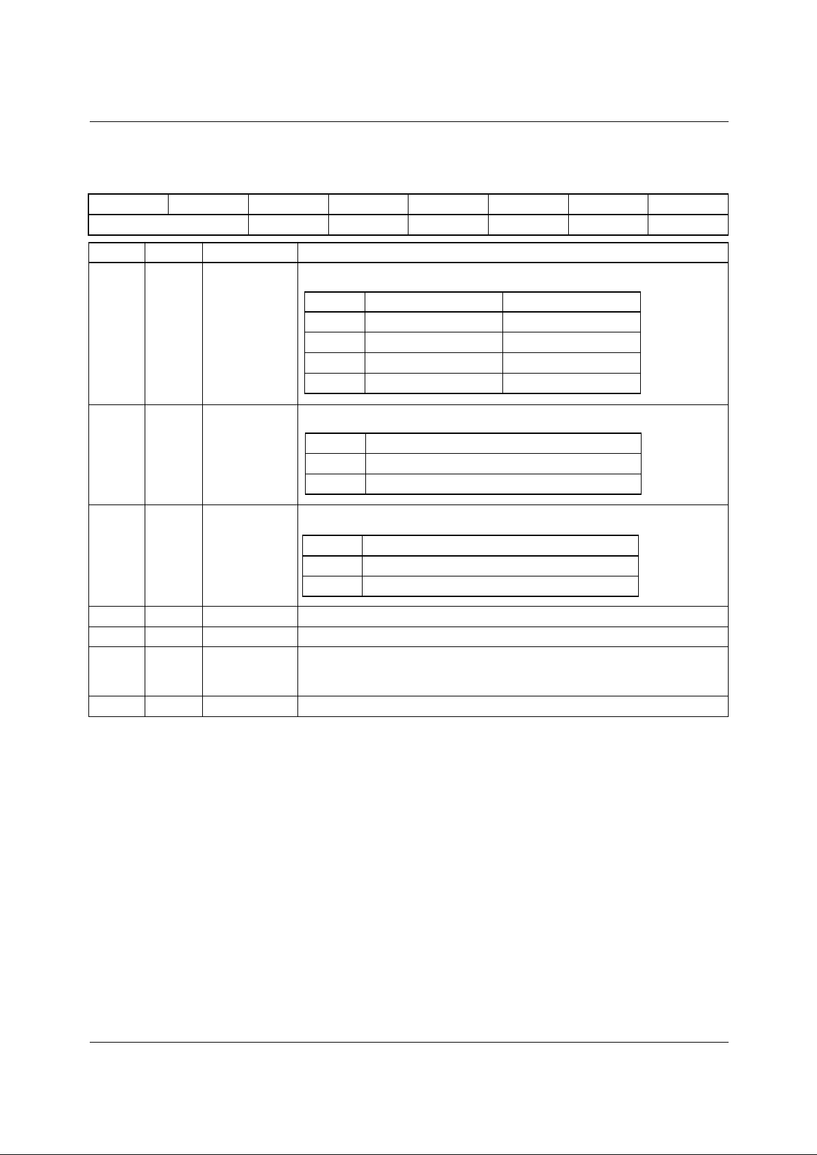
Table 1. TMC22x5yA Decoder Family................. 4
Table 2. Normalized Subcarrier Frequency
as a Function of Pixel Data Rates....... 45
Table 3. Comb Filter Architecture..................... 48
Table 4. Simple Example of an Adaptive
Comb Filter Architecture..................... 48
Table 5. Adaption Modes ...................................51
Table 6. XLUT Input Selection........................... 52
Table 7. XLUT Output Function......................... 52
Table 8. XLUT Special Function Definitions..... 52
Table 9. PAL-B,G,H,I Bruch
Blanking Sequence.............................. 53
Table 10. PAL-M Bruch Blanking Sequence ......54
Table 11. Blanking Level Selection..................... 55
Table 12. Adaptive Notch Threshold Control..... 55
Table 13. Matrix Limiters...................................... 57
Table 14. Output Format ......................................58
Table 15. NTSC Field and Line Numbering ........59
Table 16. PAL B,G,H,I Field and
Line Numbering.................................... 59
Table 17. PAL M Field and Line Numbering....... 59
Table 18. Vertical Blanking Period...................... 60
Table 19. Vertical Burst Blanking Period............ 60
Table 20. Table of Line Idents, LID[4:0].............. 60
Table 21. Timing Offsets...................................... 61
Table 22. PAL VINDO operation ..........................63
Table 23. Pixel Grab Control................................ 66
Table 24. Parallel Port Control............................. 67
Table 25. Serial Port Addresses.......................... 69
Figure 1. Logic Symbol.......................................... 4
Figure 2. Pixel Data Format................................... 4
Figure 3. Fundamental Decoder
Block Diagram...................................... 40
Figure 4. Comparison of the Frequency
Spectrum of NTSC and PAL
Composite Video Signals.................... 40
Figure 5. Examples of Notch and Bandpass
Filters..................................................... 41
Figure 6. ............................................................... 41
Figure 7. Chrominance Vector Rotation in
PAL and NTSC...................................... 42
Figure 8. Chrominance Vector Rotation Over
4 Fields in NTSC................................... 42
Figure 9. Chrominance Vector Rotation Over
4 Fields in PAL...................................... 42
Figure 10. TMC22x5yA Line Based Comb
Filter Architecture ................................43
Figure 11. Input Processor.................................... 44
Figure 12. Complementary Bandsplit Filter......... 44
Figure 13. Bandsplit Filter, Full Frequency
Response.............................................. 45
Figure 14. Bandsplit Filter, Passband
Response.............................................. 45
Figure 15. Block Diagram of Comb Filter Input... 46
Figure 16. Signal Flow Around the Adaptive
Comb Filter ...........................................47
Figure 17. Example of a Comb Fail Using a NTSC
Two Line Comb Filter........................... 49
Figure 18. Generation of Upper and Lower Comb
Fail Signals ...........................................50
Figure 19. Comb Filter Selection ..........................51
Figure 20. XLUT Input Selection ........................... 52
Figure 21. Block Diagram of Digital Burst
Locked Loop......................................... 53
Figure 22. Gaussian Low Pass Filters.................. 54
Figure 23. Gaussian LPF Passband Detail........... 54
Figure 24. Output Processor Block Diagram....... 55
Figure 25. Adaptive Notch Filters ......................... 56
Figure 26. Luminance Notch Filter .......................56
Figure 27. Horizontal Timing................................. 61
Figure 28. External HSYNC and VSYNC Timing
for Field 1(3, 5, or 7)............................. 62
Figure 29. NTSC Vertical Interval.......................... 62
Figure 30. PAL-B,G,H,I,N Vertical Interval............ 62
Figure 31. PAL-M Vertical Interval........................ 63
Figure 32. Pixel Grab Locations............................ 64
Figure 33. Relationship Between Pixel Count
and Pixel Grab Value............................ 65
Figure 34. Microprocessor Parallel Port –
Write Timing.......................................... 66
Figure 35. Microprocessor Parallel Port –
Read Timing.......................................... 68
Figure 36. Serial Port Read/Write Timing............. 69
Figure 37. Serial Interface –
Typical Byte Transfer........................... 70
Figure 38. Equivalent Digital Input Circuit........... 71
Figure 39. Equivalent Digital Output ....................71
Figure 40. Threshold Levels for Three-state........ 71
Figure 41. Input Timing Parameters ..................... 72
Figure 42. Functional Block Diagram of the
TMC22x5yA G/Y, B/U, and R/V Output
Stage...................................................... 73
Figure 43. Output Timing Parameters .................. 74
Page 4
TMC22x5yA PRODUCT SPECIFICATION
4 REV. 1.0.0 2/4/03
General Description
The TMC22x5yA digital decoder can be used as a universal
input to digital video processing systems by decoding digital
composite video and transcoding digital component inputs
into a common data format.
The digital comb filter decoder implements one of sixteen
comb filter architectures to produce luminance and color difference component signals which are virtually free of the
cross-color and cross-luminance artifacts associated with
simple bandsplit filter decoders.
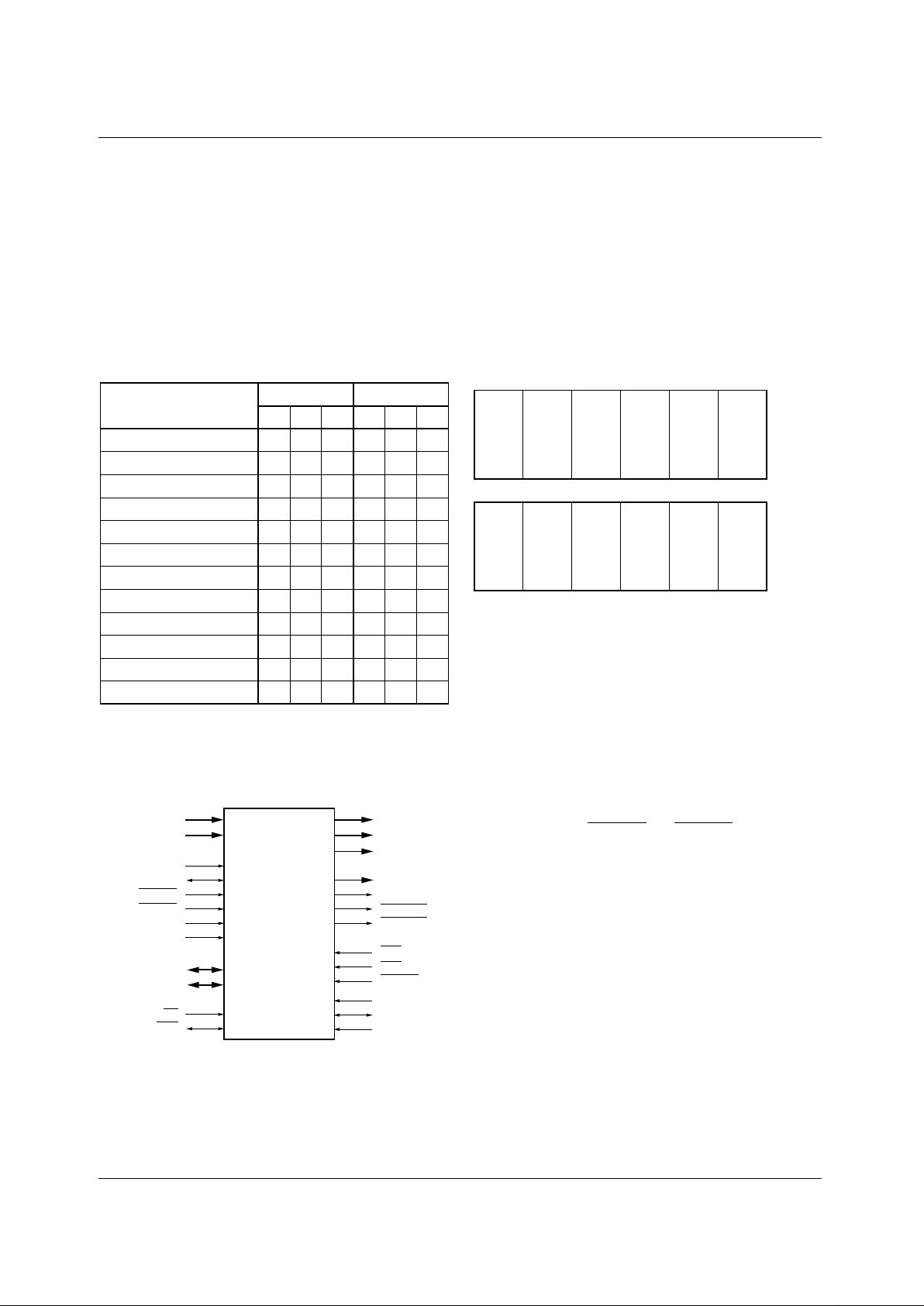
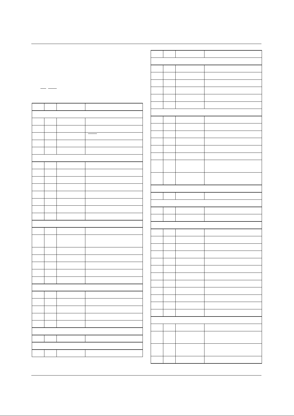
Table 1. TMC22x5yA Decoder Family
Because the cost/performance tradeoff varies among applications, the TMC22x5yA decoder has been developed as a
family of six parts. They are all assembled in the same
package, and fit the same footprint. The register maps are
identical.
Figure 1. Logic Symbol
The devices come in 8- and 10-bit resolution versions (see
Figure 2 for data alignment between 8- and 10-bit versions).
Within each resolution version there are three models, offering three-line adaptive comb filtering, two-line adaptive
comb filtering, and simple decoding. The TMC22153A
10-bit three-line comb filter can be programmed to emulate
any of the other parts. All prototyping can be performed with
this version to evaluate performance tradeoffs, and lowercost versions are easily substituted in production.
Input Processor
The digitized video and clocks provided to the decoder can
be either locked to the line frequency or the subcarrier frequency of the digitized waveform, providing broadcast quality decoding from the NTSC square pixel rate of 12.27 MHz
to the PAL four times subcarrier pixel rate of 17.73 MHz.
Figure 2. Pixel Data Format
Inputs containing embedded GRS (Fairchild Video Input
Processors), TRS words (D1 multiplexed component signals), and TRS-ID words (deserialized D2 signals) can be
used to lock the internal horizontal and vertical state
machines to the embedded information. If this information is
not provided, external horizontal and vertical syncs are
required for all line-locked input formats, and are optional
for NTSC inputs locked to four times the subcarrier (4*Fsc).
A simple sync separator is provided for digitized inputs
locked to the subcarrier frequency: the internal sync separator locks to the mid point of syncs during the vertical field
group, then flywheels during the active portion of the field.
For this reason, the DHSYNC and DVSYNC operations are
not guaranteed in subcarrier mode.
Adaptive Comb Filter
The line based adaptive comb filter in the TMC22x5yA adds
or subtracts the high frequency data from three adjacent field
lines to produce the average of the high frequency luminance
by canceling the chrominance signals, which in flat fields of
color are 180 degrees apart. Unfortunately flat fields of color
are rare and, when vertical transitions in the picture occur,
the output of the comb filter contains a mixture of both high
frequency luminance and chrominance, at which time the
comb fails. To avoid the comb filter artifacts that occur when
this happens, three sets of error signals are sent to a user-programmable lookup table, allowing the output of the comb filter to be mixed with the output of an internal bandsplit
decoder.
To produce these comb fail error signals, the video on each
of the inputs to the comb filter is passed through a simple
bandsplit decoder. The low-frequenc y portion of the signal is
TMC2215yA TMC2205yA
Function 321321
10-bit Data ✔✔✔
8-bit Data ✔✔✔✔✔✔
D1 Interface ✔✔✔✔✔✔
Line-Locked Mode ✔✔✔✔✔✔
fSC-Locked Mode ✔✔✔✔✔✔
Genlock Mode ✔✔✔✔✔✔
NTSC Frame Comb ✔✔
NTSC/PAL Field Comb ✔✔
3-Line Comb ✔✔
2-Line Comb ✔✔ ✔✔
Line Grab ✔✔ ✔✔
Pixel Grab ✔✔✔✔✔✔
65-22x5yA-02
VIDEOA
9-0
BUFFER
LDV
HSYNC
MASTER
TMC22x5yA
Multistandard
Digital
Video
Decoder
CLOCK
CS
VSYNC
R/W
D
7-0
A
1-0
VIDEOB
9-0
G/Y
9-0
B/C
B9-0
R/C
R9-0
FID
2-0
AVOUT
DHSYNC
DVSYNC
SER
SET
RESET
SA
2-0
SDA
SCL
MSB LSB
VA9
VB9
G/Y9
B/CB9
R/C
R9
VA8
VB8
G/Y8
B/C
B 8
R/C
R8
•••
VA2
VB2
G/Y2
B/CB2
R/C
R2
VA1
VB1
G/Y1
B/CB1
R/C
R1
VA0
VB0
G/Y0
B/CB0
R/C
R0
10 bit
VA9
VB9
G/Y9
B/CB9
R/C
R9
VA8
VB8
G/Y8
B/C
B 8
R/C
R8
•••
VA2
VB2
G/Y2
B/CB2
R/C
R2
N/C
N/C
N/C
N/C
N/C
N/C
N/C
N/C
N/C
N/C
8 bit
Page 5
PRODUCT SPECIFICATION TMC22x5yA
REV. 1.0.0 2/4/03 5
assumed to be luminance and the high frequency portion is
processed as chrominance to find the magnitude and phase of
the chrominance vector. These three components are then
compared across the (0H & 1H) and (1H & 2H) taps of the
comb filter to produce the difference in luminance, chrominance magnitude, and chrominance phase. These differences
are then translated in the user-programmable lookup table to
produce the “K” signal which controls the complementary
mix between the output of the comb filter and the simple
bandsplit decoder. That is, the “K” signals controls how
much of the combed high frequency luminance signal is subtracted from the simple bandsplit chrominance for chroma
combs, or added to the low frequency output of the bandsplit
for luma comb filters.
Output Processor
The demodulated chrominance signal and the luminance
signal are passed through a programmable output matrix,
producing RGB, YUV, or YCBCR. When the clock is at
27MHz, a D1 signal can be produced on the R/V output with
the embedded TRS words fixed to the external HSYNC and
VSYNC timing.
Parallel and Serial Microprocessor Interfaces
The parallel microprocessor interface employs 12 pins, the
serial port uses 5. A single pin, SER
, selects between the two
interface modes.
In parallel interface mode, one address line is decoded for
access to the internal control register and its pointer.
Controls are reached by loading a desired address through
the 8-bit D
7-0
port, followed by the desired data (read or
write) for that address. The control register address pointer
auto-increments to address 3Fh and then remains there.
A 2-line serial interface may also be used for initialization
and control. The same set of registers accessed by the parallel port is available to the serial port. The device address in
the serial interface is selected via pins SA
2-0
.
The RESET pin sets all internal state machines to their initialized conditions and places the decoder in a power-down
mode. All register data are maintained while in power-down
mode.
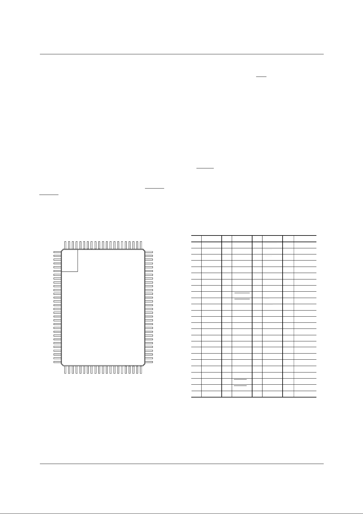
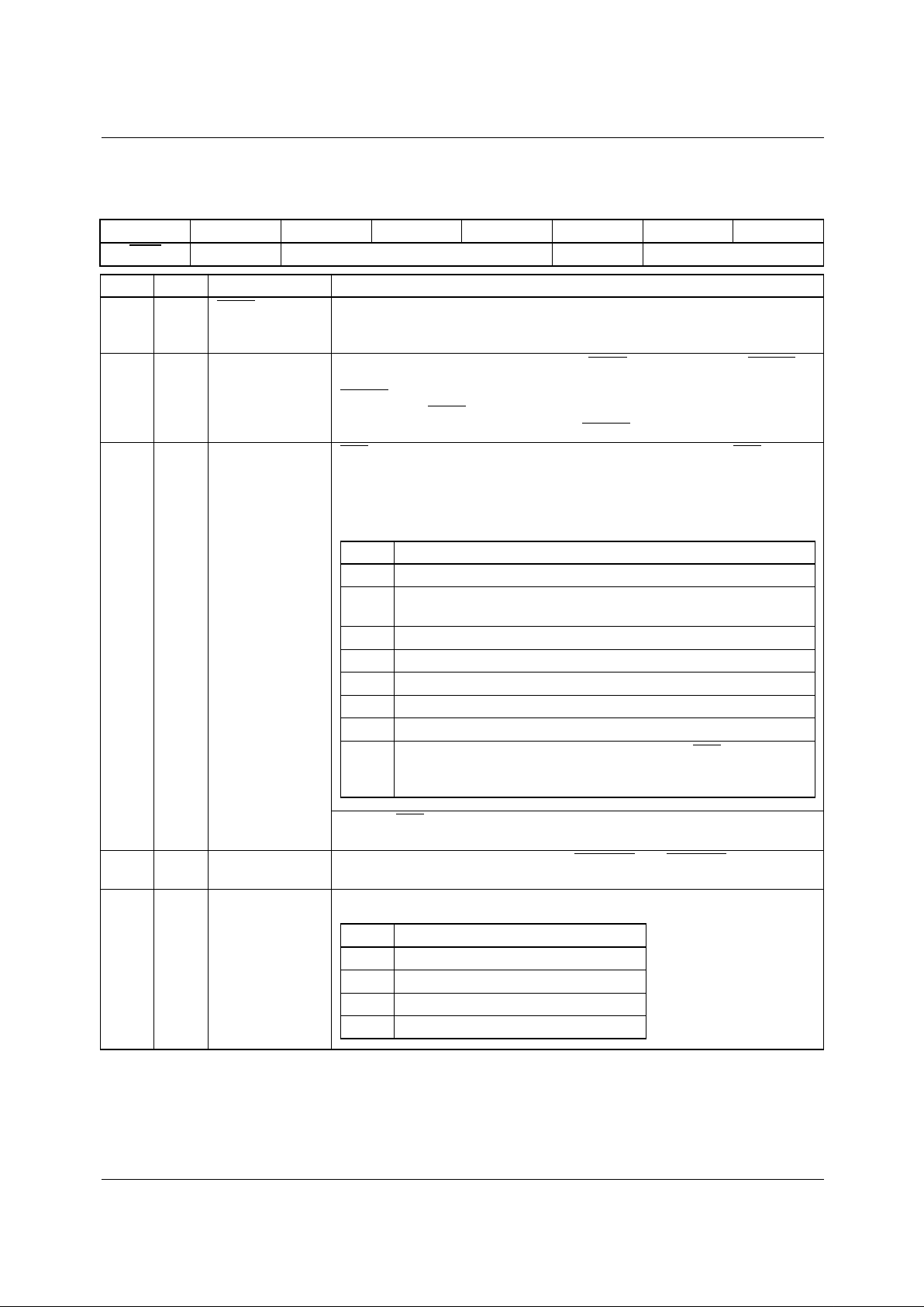
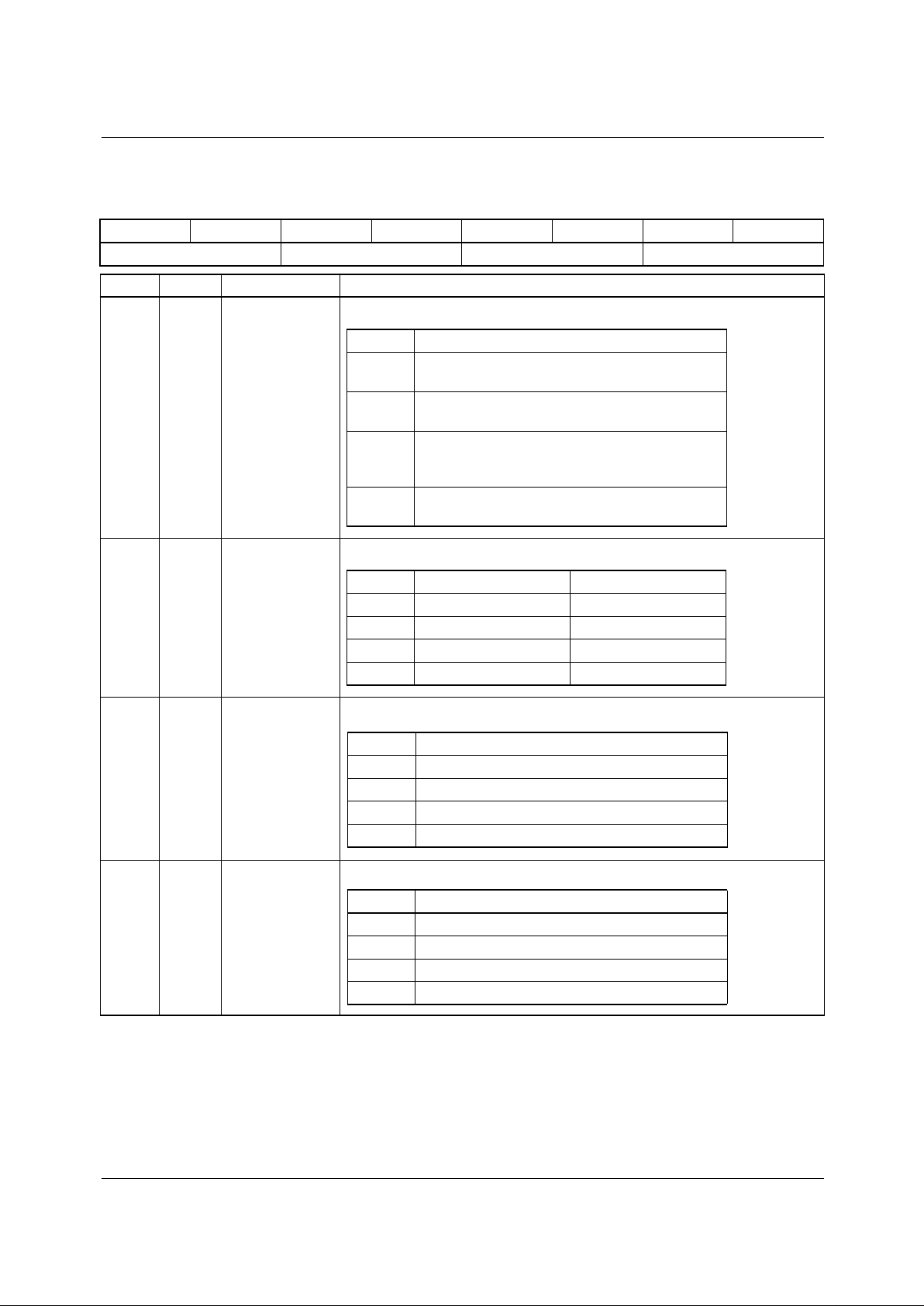
Pin Assignments
G/Y
1
G/Y
0
LDV
GND
V
DD
B/Cb
9
B/Cb
8
B/Cb
7
B/Cb
6
B/Cb
5
B/Cb
4
B/Cb
3
B/Cb
2
B/Cb
1
B/Cb
0
GND
V
DD
R/Cr
9
R/Cr
8
R/Cr
7
R/Cr
6
R/Cr
5
R/Cr
4
R/Cr
3
R/Cr
2
1
2
3
4
5
6
7
8
9
10
11
12
13
14
15
16
17
18
19
20
21
22
23
24
25
R/Cr
1
R/Cr
0
GND
V
DD
DREF
FID
0
FID
1
FID
2
DHSYNC
DVSYNC
D
0
D
1
D
2
GND
V
DD
D
3
D
4
D
5
D
6
D
7
GND
V
DD
HSYNC
VSYNC
BUFFER
26
27
28
29
30
31
32
33
34
35
36
37
38
39
40
41
42
43
44
45
46
47
48
49
50
Pin Name Pin Name
RESET
SET
SER
SA
0
SA
1
SA
2
GND
SDA
SCL
CS
R/W
A
0
A
1
GND
V
DD
VIDEOB
0
VIDEOB
1
VIDEOB
2
VIDEOB
3
VIDEOB
4
VIDEOB
5
VIDEOB
6
VIDEOB
7
VIDEOB
8
VIDEOB
9
51
52
53
54
55
56
57
58
59
60
61
62
63
64
65
66
67
68
69
70
71
72
73
74
75
GND
VIDEOA
0
VIDEOA
1
VIDEOA
2
VIDEOA
3
VIDEOA
4
VIDEOA
5
VIDEOA
6
VIDEOA
7
VIDEOA
8
VIDEOA
9
MASTER
0
MASTER
1
CLOCK
GND
V
DD
GND
G/Y
9
G/Y
8
G/Y
7
G/Y
6
G/Y
5
G/Y
4
G/Y
3
G/Y
2
76
77
78
79
80
81
82
83
84
85
86
87
88
89
90
91
92
93
94
95
96
97
98
99
100
Pin Name Pin Name
1
30
65-22x5y-03
31 50
51
80
81100
Page 6
TMC22x5yA PRODUCT SPECIFICATION
6 REV. 1.0.0 2/4/03
Pin Descriptions
Pin Name Pin Number Value Pin Function Description
Inputs
VIDEOA
9-0
86, 85, 84, 83,
82, 81, 80, 79,
78, 77
TTL Video input A. An 8 or 10 bit data input to the input multiplexer.
For 8-bit versions (TMC2205yA) the data are left-justified (VIDEOA
9-2
).
VIDEOB
9-0
75, 74, 73, 72,
71, 70, 69, 68,
67, 66
TTL Video input B. An 8 or 10 bit data input to the input multiplexer.
For 8-bit versions (TMC2205yA) the data are left-justified (VIDEOB
9-2
).
VSYNC 49 TTL Vertical sync input. A vertical sync signal (active low) occurring at the
start of the first vertical sync pulse in a vertical field group. A falling edge
of VSYNC
which is coincident with a falling edge of HSYNC indicates
field 1. This signal is active only when SPGIP
1-0
= 00.
HSYNC 48 TTL Horizontal sync input. A horizontal sync signal (active low) occurring
at the falling edge of the video sync. This signal is active only when
SPGIP
1-0
= 00.
MASTER
1-0
88, 87 TTL Master decoder control.
00 Adaptive comb decoder
01 Simple bandsplit decoder
10 Reserved
11 Flat notched luma and simple bandsplit chroma
BUFFER 50 TTL Control register select. This signal switches between two sets of
registers which control the gain or hue values in the output matrix.
When BUFFER = 0, registers 17-1F are active. When BUFFER = 1,
registers 27-2F take control.
CLOCK 89 TTL Master processing clock. The clock signal can either be at twice the
pixel data rate in the line locked modes, or at four times the subcarrier
frequency in the subcarrier mode. The interpretation of the CLOCK
signal is set by the CKSEL register bit.
SET 52 TTL Programmable function pin. The function specified by the SET
register is active when SET is low. The decoder returns to its previous
operation when SET goes high.
Outputs
G/Y
9-0
93, 94, 95, 96,
97, 98, 99, 100,
1, 2
TTL Green or Luminance digital output. For 8-bit versions (TMC2205yA)
the data are left-justified (G/Y
9-2
).
B/C
B9-0
6, 7, 8, 9, 10,
11, 12, 13, 14,
15
TTL Blue or CB digital output. For 8-bit versions (TMC2205y) the data are
left-justified (B/C
B 9-2
).
R/C
R9-0
18, 19, 20, 21,
22, 23, 24, 25,
26, 27
TTL Red or CR digital output. For 8-bit versions (TMC2205yA) the data are
left-justified (R/C
R 9-2
).
DVSYNC 35 TTL Vertical sync output. The DVSYNC signal occurs once per field and
lasts for 1 video line.
DHSYNC 34 TTL Horizontal sync output. The DHSYNC signal occurs once per line and
lasts for 64 clock periods.
LDV 3 TTL Data synchronization output. LDV can be an internally or externally
generated clock signal. The internal LDV signal is produced when the
CLOCK input is at twice the pixel data rate (PXCK); and is a pixel data
rate clock phase locked to the falling edge of the HSYNC. The external
LDV can be selected under software control, and must be at the
CLOCK, or a sub multiple of the CLOCK, frequency.
Page 7
PRODUCT SPECIFICATION TMC22x5yA
REV. 1.0.0 2/4/03 7
DREF 30 TTL Decoder reference signal. This is a dual function pin, controlled by
register 24, that can function as an active video output indicator or
output as a clamp pulse. When set to the active video output function,
the DREF pin is HIGH during the video portion of each line and LOW
during the horizontal and vertical blanking levels. When set to output a
clamp pulse, the clamp pulse is controlled by register 24 and 25
allowing a user to program when a 0.5 µSec pulse is output relative to
HSYNC.
FID
2-0
33, 32, 31 TTL Field identification output. A 3 bit field ident from the DRS signal.
µP Interface
D
7-0
45, 44, 43, 42,
41, 38, 37, 36
TTL Parallel control port data I/O. All control parameters are loaded into
and read back over this 8 bit data port.
A
1-0
63, 62 TTL Parallel control port address inputs. These pins govern whether the
microprocessor interface selects a table/register address or reads/
writes table/register contents.
CS 60 TTL Parallel control port chip select. When CS is high the microprocessor
interface port, D
7-0
, is set to HIGH impedance and ignored. When CS
is LOW, the microprocessor can read or write parameters over D
7-0
.
R/W 61 TTL Parallel control port read/write control. When R/W and CS are LOW,
the microprocessor can write to the control registers or XLUT over
D
7-0
. When R/W is HIGH and CS is LOW, it can read the contents of
any selected XLUT address or control register over D
7-0
.
RESET 51 TTL Chip master reset. Bringing RESET LOW sets the software reset
control bit, SRESET, LOW and disables the digital outputs. If HRESET
is LOW the decoder outputs remain disabled after RESET goes HIGH
until the SRESET bit is set high by the host. If HRESET is HIGH when
RESET goes HIGH the decoder the internal state machines are
enabled.
SER 53 TTL Serial/parallel interface select. This pin will select between a parallel
(HIGH) or serial (LOW) interface port.
SDA 58 R-Bus Serial data interface. Bi-directional serial interface to the control port.
SCL 59 R-Bus Serial interface clock.
SA
2-0
56, 55, 54 TTL Serial Address. Three bits providing the lsbs of the serial chip ID used
to identify the decoder.
Power Supply
V
DD
5, 17, 29, 40,
47, 65, 91
+5 V Power Supply. Positive power supply for digital circuits, +5V.
GND 4, 16, 28, 39,
46, 57, 64, 76,
90, 92
0.0 V Ground. Ground for digital circuits, 0V.
Pin Descriptions (cont.)
Pin Name Pin Number Value Pin Function Description
Page 8
TMC22x5yA PRODUCT SPECIFICATION
8 REV. 1.0.0 2/4/03
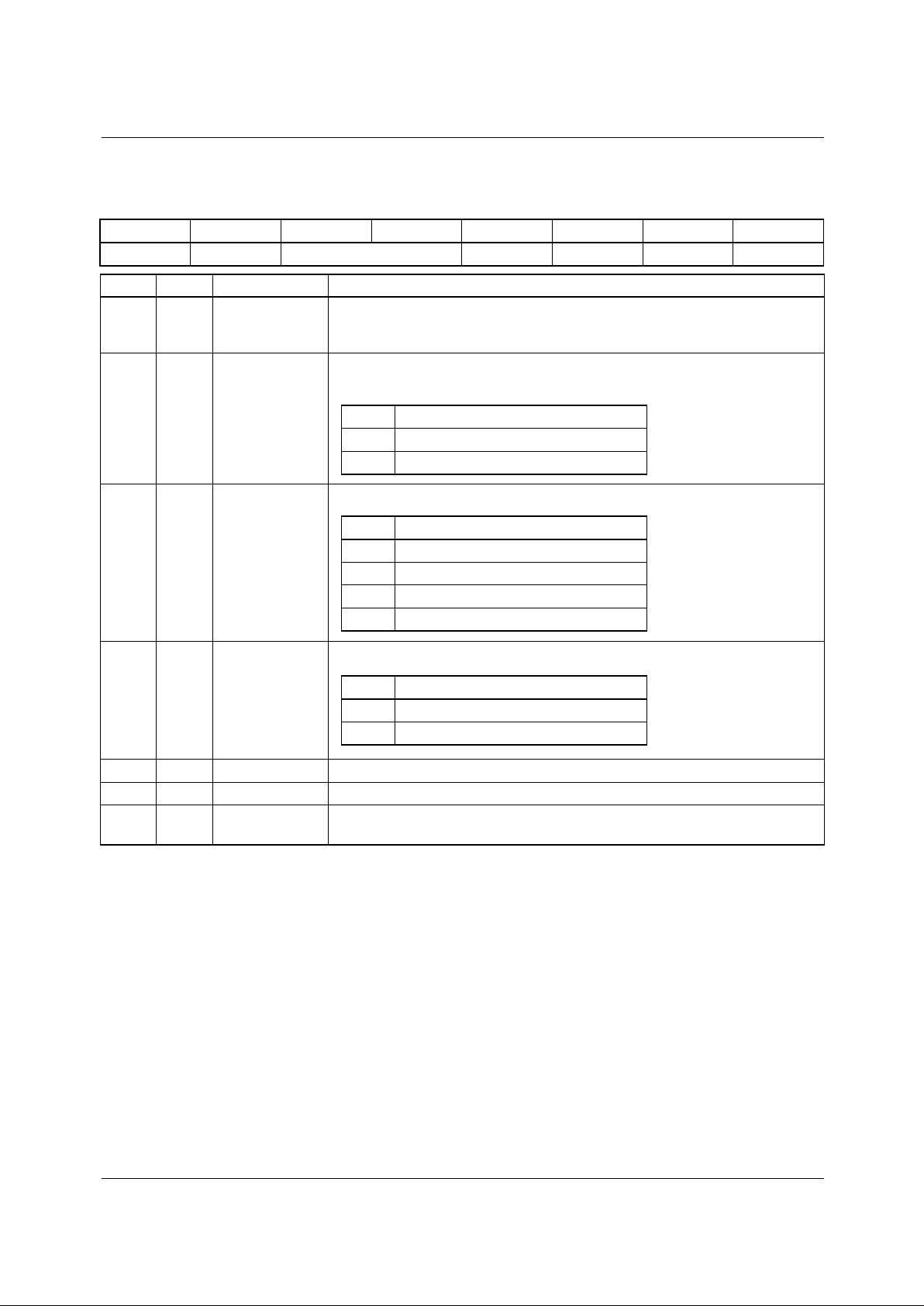
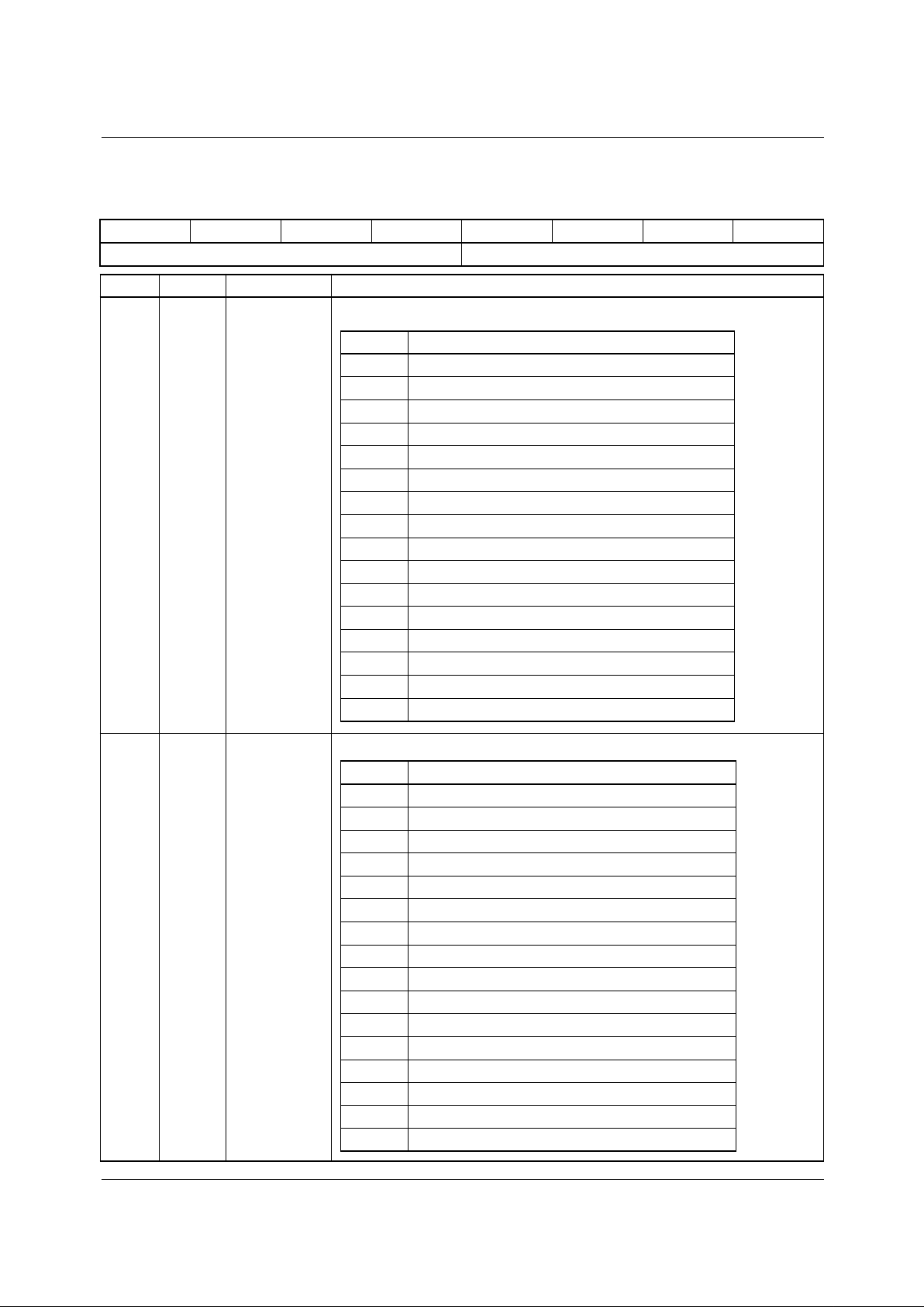
Control Register Map
The TMC22x5yA is initialized and controlled by a set of
registers which determine the operating modes.
An external controller is employed to write and read the
Control Registers through either the 8-bit parallel or 2-line
serial interface port. The parallel port, D
7-0
, is governed by
pins CS
, R/W , and A
1-0
. The serial port is controlled by SDA
and SCL.
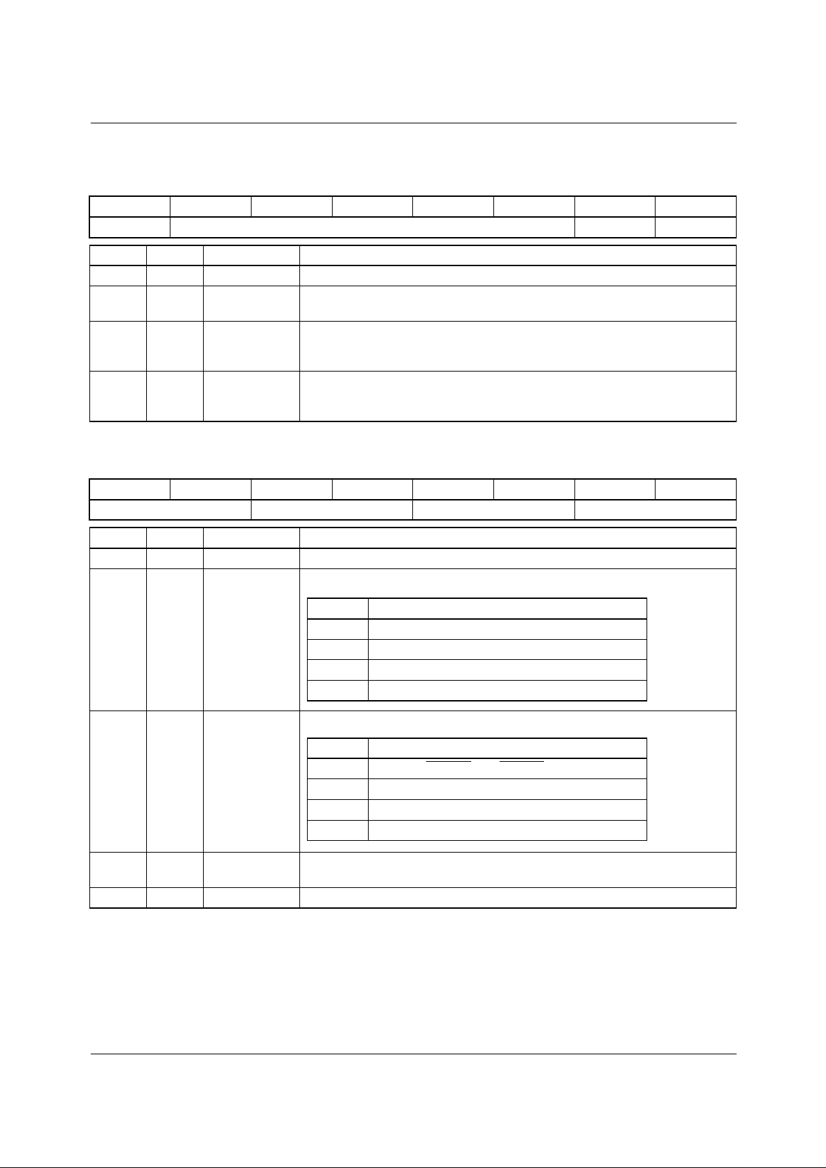
Reg Bit Name Function
Global Control
00 7 SRST Software reset
00 6 HRST Hardware reset
00 5-3 SET SET
pin function
00 2 DHVEN Output H&V sync enable
00 1-0 STD Selects video standard
Input Processor Control
01 7 reserved, set to zero
01 6 IPMUX Input mux control
01 5 IP8B 8 bit input format
01 4 TDEN TRS detect enable
01 3 TBLK TRS blank enable
01 2 IPCMSB Chroma input msb invert
01 1 ABMUX AB mux control
01 0 CKSEL Input clock rate select
Burst Loop Control
02 7 BLLRST BLL auto. reset enable
02 6 VIPEN Video Input Processor
enable
02 5-4 LOCK Global lock mode
02 3 BLM BLL lock mode
02 2 KILD Color kill disable
02 1 DMODBY Demod bypass
02 0 CINT CBCR interpolation enable
Chroma Processor Control
03 7-5 BLFS Burst loop filter select
03 4 CCEN Chroma coring enable
03 3-2 CCOR Chroma coring threshold
03 1 GAUBY Gaussian filter bypass
03 0 GAUSEL Gaussian filter select
Burst Threshold
04 7-0 BTH Burst threshold
Pedestal
05 7-0 PED Pedestal level
Luma Processor Control
06 7-6 reserved, set to zero
06 5 ANEN Adaptive notch enable
06 4 ANR Adaptive notch rounding
06 3-2 ANT Adaptive notch threshold
06 1 ANSEL Adaptive notch select
06 0 NOTCH Notch enable
Comb Processor Control
07 7 LS1BY Line store 1 bypass
07 6 LS1IN Line store 1 input
07 5 LS2DLY Line store 2 delay
07 4 SPLIT Line store 2 data width
07 3 BSFBY Bandsplit filter bypass
07 2 BSFSEL Bandsplit filter select
07 1 BSFMSB Inverts msb of bandsplit
filter
07 0 GRSDLY Delays input to GRS
decode by 1H
Mid-Sync Level
08 7-0 MIDS Mid-sync level
Extended DRS
09 7-4 PCKF Clock rate
09 3-0 VSTD Video standard
Output Control
0A 7 OP8B Output rounded to 8 bits
0A 6-5 OPLMT Output limit select
0A 4-3 MSEN Mixed sync enable
0A 2 OPCMSB Chroma output msb invert
0A 1 YBAL Luma color correction
0A 0 BUREN Output burst enable
0B 7 FMT422 Enables C
BCR
output mux
0B 6 CDEC CBCR decimation enable
0B 5 YUVT Enables D1 output
0B 4-2 reserved, set to zero
0B 1 DRSEN DRS output enable
0B 0 DRSCK DRS data rate
Comb Filter Control
0C 7-6 ADAPT Adaption mode
0C 5 YCES YC input error signal
control
0C 4 YCSEL luma/chroma comb filter
select
0C 3-0 COMB Comb filter architecture
Reg Bit Name Function
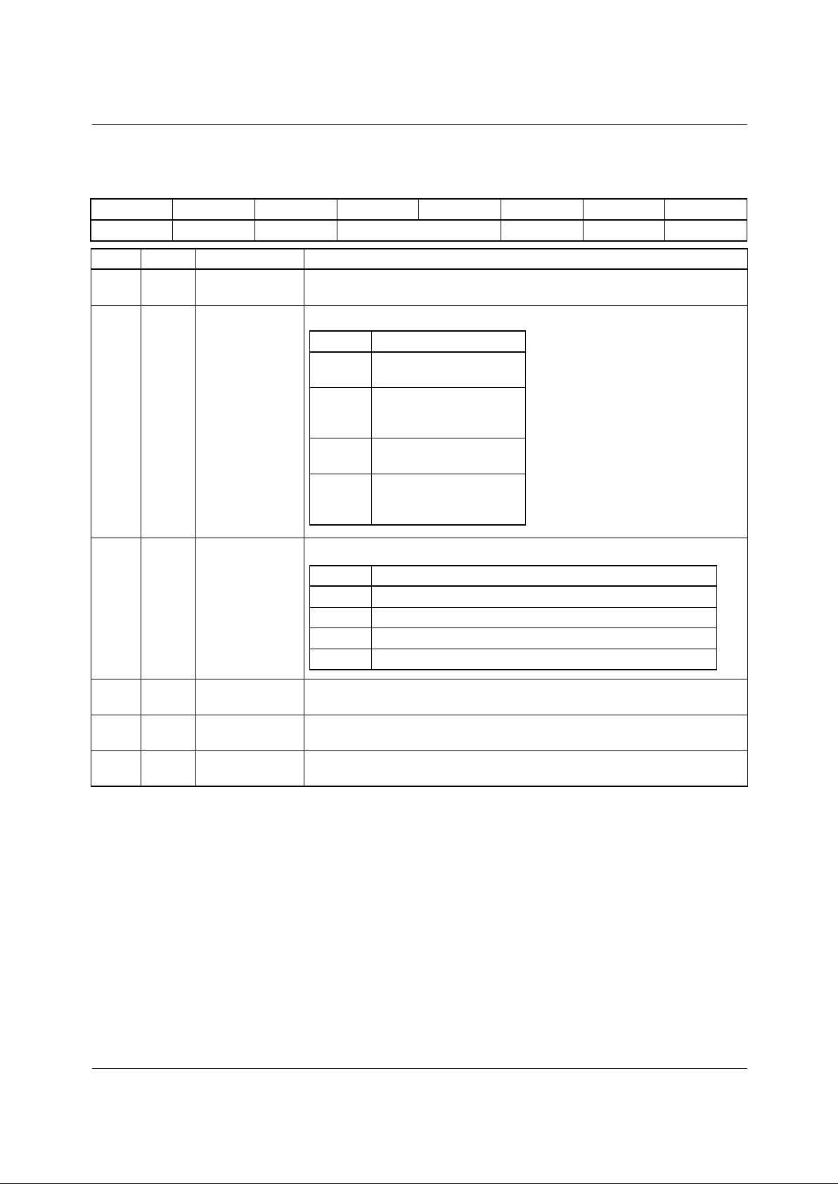
Page 9

PRODUCT SPECIFICATION TMC22x5yA
REV. 1.0.0 2/4/03 9
0D 7-6 CEST Chroma error signal
transform
0D 5 CESG Chroma error signal gain
0D 4 YESG Luma error signal gain
0D 3 CESTBY Chroma error signal
bypass
0D 2 XFEN XLUT filter enable
0D 1 FAST Adaption speed select
0D 0 YWBY Luma weighting bypass
0E 7-6 XIP XLUT input select
0E 5-4 XSF XLUT special function
0E 3-2 YMUX Y output select
0E 1-0 CMUX C output select
0F 7 reserved, set to zero
0F 6-5 CAT Adaption Threshold
0F 4 DCES D1 C
BCR
error signal
0F 3-2 IPCF Comb filter input select
0F 1 YCCOMP YC or Composite input
select
0F 0 SYNC Sync processor select
Sync Pulse Generator
10 7-0 STS
7-0
Sync to sync 8 lsbs
11 7-0 STB Sync to burst
12 7-0 BTV Burst to video
13 7-0 AV
7-0
Active video line 8 lsbs
14 7-6 reserved, set to zero
14 5-4 AV
9-8
Active video line 2 msbs
14 3 reserved, set to zero
14 2-0 STS
10-8
Sync to sync 3 msbs
15 7 reserved, set to zero
15 6-2 VINDO Number of lines in vertical
window
15 1 VDIV Action inside VINDO
15 0 VDOV Action outside VINDO
16 7-6 reserved, set to zero
16 5-4 NFDLY new field detect delay
16 3-2 SPGIP SPG input select
16 1-0 MSIP Mixed sync separator input
select
Buffered register set 0
Active when BUFFER pin set LOW
17 7-0 SG0
7-0
Msync gain, 8 lsbs
18 7-0 YG0
7-0
Y gain, 8 lsbs
19 7-0 UG0
7-0
U gain, 8 lsbs
Reg Bit Name Function
1A 7-0 VG0
7-0
V gain, 8 lsbs
1B 7-6 YG0
9-8
Y gain, 2 msbs
1B 5-3 UG0
10-8
U gain, 3 msbs
1B 2 reserved, set to zero
1B 1-0 VG0
9-8
V gain, 2 msbs
1C 7-0 YOFF0
7-0
Y offset, 8 lsbs
1D 7-3 reserved, set to zero
1D 2 YOFF0
8
Y offset, msb
1D 1-0 SG0
7-0
Msync gain, 2 msbs
1E 7-1 SYSPH0
6-0
7 lsbs of phase
1E 0 VAXISO V axis flip
1F 7-0 SYSPH0
14-7
8 msbs of phase
Normalized Subcarrier Frequency
20 7-4 FSC
3-0
Bottom 4 bits of f
SC
20 3-0 reserved, set to zero
21 7-0 FSC
11-4
Lower 8 bits of f
SC
22 7-0 FSC
19-12
Middle 8 bits of f
SC
23 7-0 FSC
27-20
Top 8 bits of f
SC
Clamp Control
24 7 DRFSEL Clamp pulse enable
24 6 PFLTBY Phase filter enable
24 5-4 CLPSEL
1-0
Int. clamp selection
24 3 VCLPEN Clamp bypass
24 2-0 BAND
2-0
Clamp offset
25 7-0 CPDLY
7-0
Clamp pulse delay
Output Format Control
26 7-6 reserved, set to zero
26 5 LDVIO LDV clock select
26 4 OPCKS Output clock select
26 3 DPCEN DPC enable
26 2-0 DPC Decoder product code
Buffered register set 1
Active when BUFFER pin set HIGH
27 7-0 SG1
7-0
Msync gain, 8 lsbs
28 7-0 YG1
7-0
Y gain, 8 lsbs
29 7-0 UG1
7-0
U gain, 8 lsbs
2A 7-0 VG1
7-0
V gain, 8 lsbs
2B 7-6 YG1
9-8
Y gain, 2 msbs
2B 5-3 UG1
10-8
U gain, 3 msbs
2B 2 reserved, set to zero
2B 1-0 VG1
9-8
V gain, 2 msbs
2C 7-0 YOFF1
7-0
Y offset, 8 lsbs
2D 7-3 reserved, set to zero
Reg Bit Name Function
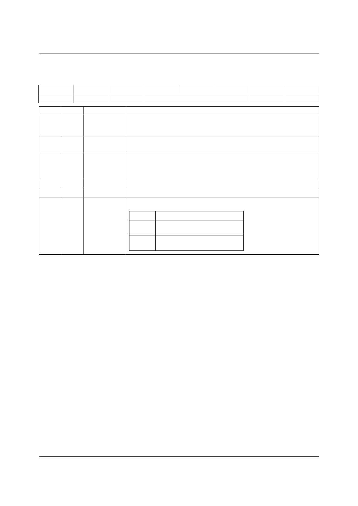
Page 10
TMC22x5yA PRODUCT SPECIFICATION
10 REV. 1.0.0 2/4/03
2D 2 YOFF1
8
Y offset, msb
2D 1-0 SG1
7-0
Msync gain, 2 msbs
2E 7-1 SYSPH1
6-0
7 lsbs of phase
2E 0 VAXIS1 V axis flip
2F 7-0 SYSPH1
14-7
8 msbs of phase
Video Measurement
30 7 set to zero
30 6 LGF Line grab flag
30 5 LGEN Line grab enable
30 4 LGEXT Ext line grab enable
30 3 reserved, set to zero
30 2 PGG Pixel grab gate
30 1 PGEN Pixel grab enable
30 0 PGEXT Ext pixel grab enable
31 7-0 PG
7-0
Pixel grab, 8 lsbs
32 7-0 LG
7-0
Line grab, 8 lsbs
33 7 reserved, set to zero
33 6-4 FG Field grab number
33 3 LG
8
Msb of line grab
33 2-0 PG
10-8
Pixel grab, 3 msbs
34 7-0 GY
9-2
G/Y grab, 8 msbs
35 7-0 BU
9-2
B/U grab, 8 msbs
36 7-0 RV
9-2
R/V grab, 8 msbs
37 7-6 reserved
37 5-4 GY
1-0
G/Y grab, 2 lsbs
37 3-2 BU
1-0
B/U grab, 2 lsbs
37 1-0 RV
1-0
R/V grab, 2 lsbs
38 7-0 Y
9-2
Luma grab, 8 msbs
39 7-0 M
9-2
Msync grab, 8 msbs
3A 7-0 U
9-2
U grab, 8 msbs
3B 7-0 V
9-2
V grab, 8 msbs
3C 7-6 Y
1-0
Luma grab, 2 lsbs
3C 5-4 M
1-0
Msync grab, 2 lsbs
3C 3-2 U
1-0
U grab, 2 lsbs
3C 1-0 V
1-0
V grab, 2 lsbs
Test Control
3D 7-0 TEST Must be set to zero
3E 7-0 TEST Must be set to zero
Vertical Blanking Control
3F 7 VBIT20 V bit control
3F 6 PEDDIS Pedestal control
3F 5-0 CCDEN
5-0
Closed caption control
Auto-increment stops at 3F
Reg Bit Name Function
Notes:
1. Functions are listed in the order of reading and writing.
2. For each register listed above up to register 3F, all bits not
specified are reserved and must be set to zero to ensure
proper operation.
Status - Read Only
40 7-0 DDSPH DDS phase, 8 msbs
41 7 LINEST Pixel count reset
41 6 BGST Start of burst gate
41 5 VACT2 Half line flag
41 4 PALODD PAL Ident
41 3 VFLY Vertical count reset
41 2 FGRAB Field grab
41 1 LGRAB Line grab
41 0 PGRAB Pixel grab
42 7 FLD Field flag (F in D1 output)
42 6 VBLK Vertical blanking (V in D1
output)
42 5 HBLK Horizontal blanking (H in
D1 output)
42 4-0 LID Line identification
43 7 YGO Y/G overflow
43 6 YGU Y/G underflow
43 5 UBO C
B
/B overflow
43 4 UBU CB/B underflow
43 3 VRO CR/R overflow
43 2 VRU CR/R underflow
43 1-0 reserved
44 7 MONO Color kill active
44 6-0 FPERR Frequency/Phase error
45 7-0 DRS DRS signal
46 7-0 PARTID Reads back xx
h
47 7-0 REVID Revision number
48-4A7-0 reserved
4B 7 PKILL Phase kill from comb fail
4B 6-5 CFSTAT Comb filter status
4B 4-0 XOP XLUT output
4C-FF7-0 reserved
Reg Bit Name Function
Page 11
PRODUCT SPECIFICATION TMC22x5yA
REV. 1.0.0 2/4/03 11
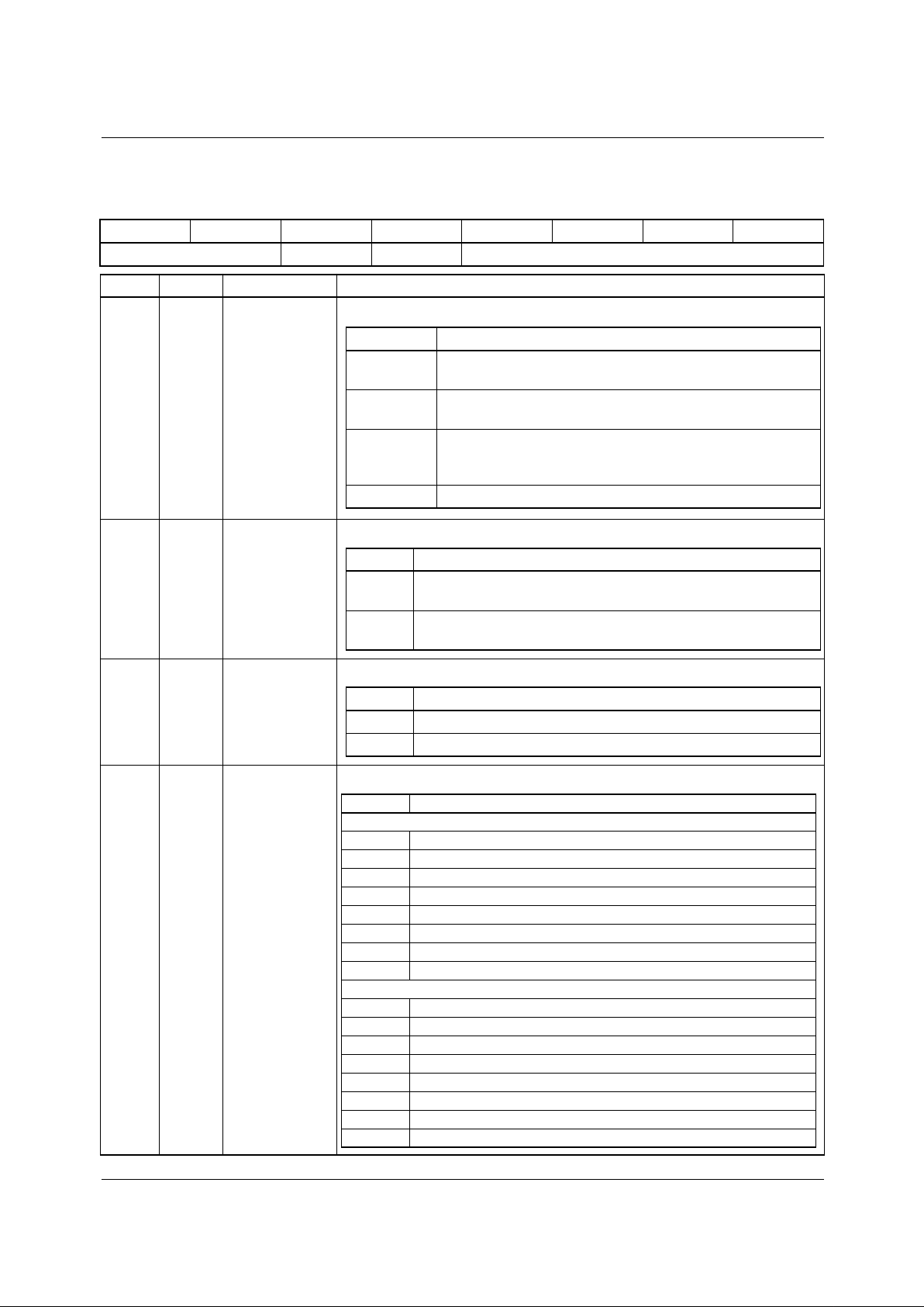
Control Register Definitions
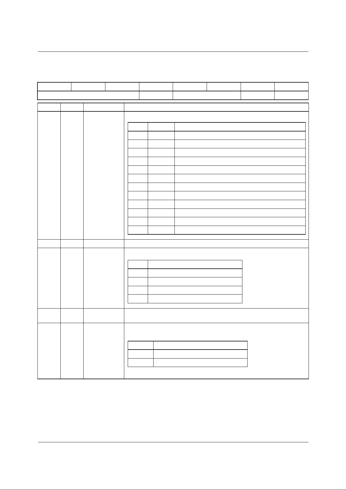
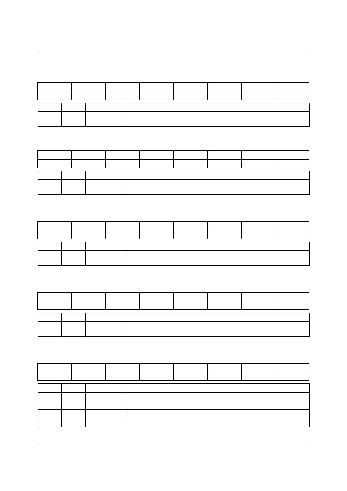
Global Control Register (00)
76543210
SRST
HRST SET DHVEN STD
Reg Bit Name Description
00 7 SRST Software reset. When LOW, resets and holds internal state machines and
disables outputs. When HIGH (normal), starts and runs state machines and
enables outputs. This bit is ignored while HRST is high.
00 6 HRST Hardware reset. When HRST is HIGH, SRST
is forced low when RESET pin
is taken LOW. State machines are reset and held. When HRST is low the
RESET
pin can be taken HIGH at any time. The state machines remain
disabled until SRST is programmed HIGH. When HRST is high the state
machines are enabled as soon as the RESET pin goes HIGH.
00 5-3 SET SET pin function. These bits control the set function when the SET pin goes
low.
A = all outputs high-impedance
B = internal state machines
C = burst locked loop
The first SET pulse after a software or hardware reset, with SET = 111,
causes a toggle to SET = 010.
00 2 DHVEN Output H&V sync enable. Disables DHSYNC and DVSYNC signals when
HIGH.
00 1-0 STD Selects video standard. Selects video standard.
SET Function
000 Reset and hold A, B, & C.
001 Set output to BLUE and flywheel B & C. (RGB outputs)
Set output to "color" and flywheel B & C (YCBCR outputs)
010 Hold A, lock B & C to external input
011 Reset C only
100 Reset B & C
101 Set output to BLUE and lock B & C to input video (RGB output)
110 Line and pixel grab depending on VMCR
6-0
(reg 30)
111 Toggle reset function of SET = 010. For each SET = 0 pulse the
chip operation will change from normal to that of SET = 010 or
visa versa.
SET Function
00 NTSC
01 reserved
10 PAL/M
11 All PAL standards except PAL/M
Page 12

TMC22x5yA PRODUCT SPECIFICATION
12 REV. 1.0.0 2/4/03
Control Register Definitions (continued)
Input Processor Control (01)
76543210
Reserved IPMUX IP8B TDEN TBLK IPCMSB ABMUX CKSEL
Reg Bit Name Description
01 7 Reserved Reserved, set to zero.
01 6 IPMUX Input mux control. Used to select the Video Input Processor, D1, or D2 data
as the VA input to the input processor.
VIDEOA is selected for VA and VIDEOB is selected for VB when IPMUX is
set LOW. VIDEOB is selected for VA and VIDEOA for VB when IPMUX is set
HIGH. For YC inputs, the luma data must be passed through the VA input and
chroma through the VB input.
IPMUX should be set LOW for line locked composite inputs.
01 5 IP8B 8 bit input format. Bottom two bits of inputs VIDEOA
9-0
and VIDEOB
9-0
are
set to zero when HIGH.
01 4 TDEN TRS detect enable. When HIGH, the TRS words embedded in incoming
video are used to reset the horizontal and vertical state machines. When LOW
the externally provided or internally generated HSYNC and VSYNC are used
to reset the horizontal and vertical state machines.
01 3 TBLK TRS blank enable. Blanks the TRS and AUX data words when HIGH. For line
locked and D1 data, the TRS and AUX data words are set to the luma and
chroma blanking levels as appropriate. For D2 (4*fSC) data, the TRS and
AUX data words are set to the sync tip level.
01 2 IPCMSB Chroma input msb invert. The msb of the chroma or CBCR data are inverted
when HIGH.
01 1 ABMUX AB mux control. Selects the primary and secondary inputs to the decoder
from the DA and DB outputs of the input processor. When ABMUX is LOW,
DA is selected as the primary and DB as the secondary decoder input.
01 0 CKSEL Input clock rate select. Set HIGH for line locked clocks and LOW for
subcarrier locked clocks. Line locked clocks should be at twice the pixel data
rate, and the subcarrier clock should be at four times the subcarrier
frequency.
Page 13
PRODUCT SPECIFICATION TMC22x5yA
REV. 1.0.0 2/4/03 13
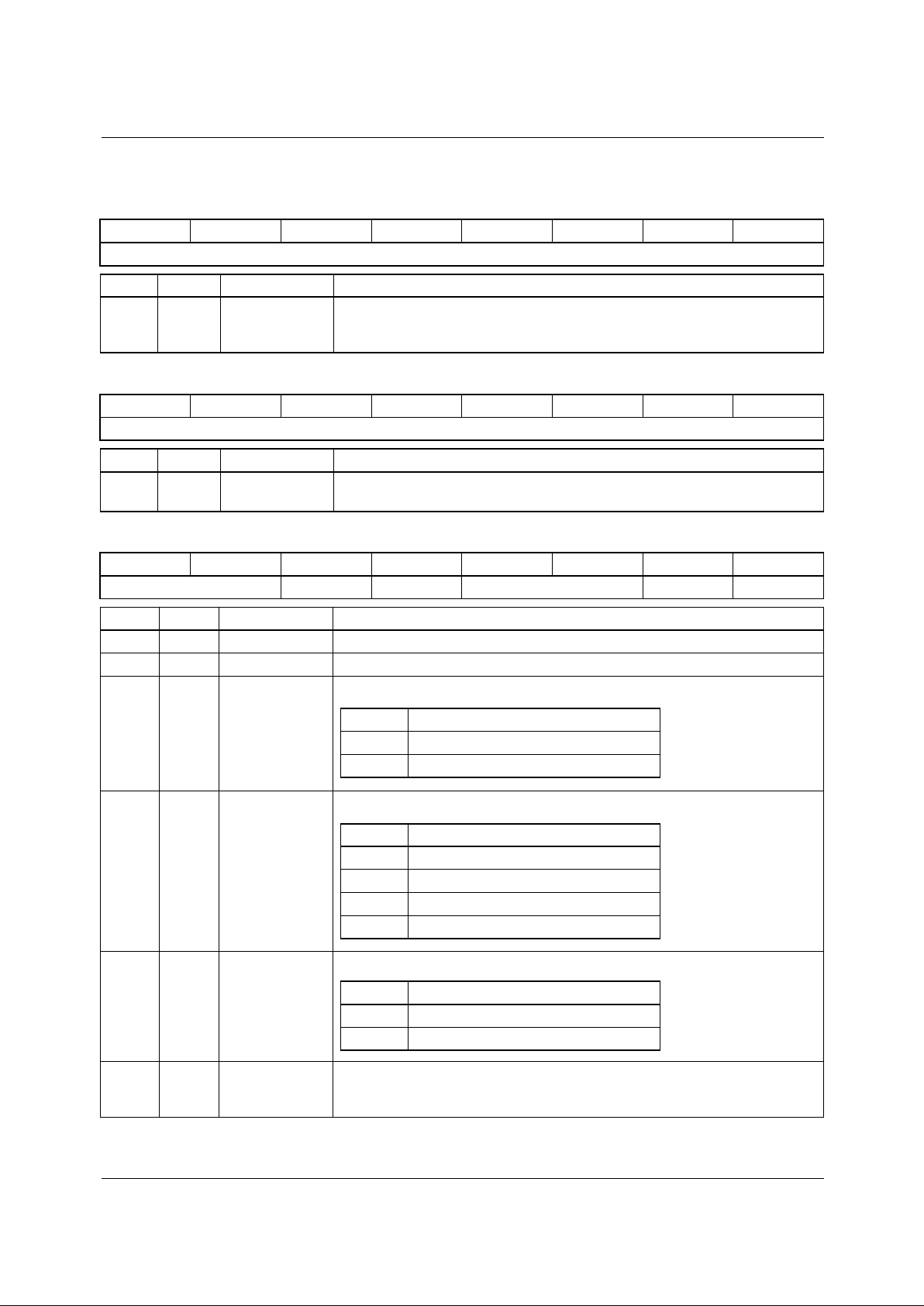
Control Register Definitions (continued)
Burst Loop Control (02)
76543210
BLLRST VIPEN LOCK BLM KILD DMODBY CINT
Reg Bit Name Description
02 7 BLLRST BLL reset enable. When LOW, the automatic BLL reset is disabled. When
HIGH, the BLL will be reset if the BLL loses lock and fails to reacquire lock
within 8 fields.
02 6 VIPEN Video Input Processor enable. Selects interface protocol for Fairchild video
input devices. Active only when LOCK
1-0
= 10.
02 5-4 LOCK Global Lock mode. Sets the decoder locking mode.
02 3 BLM BLL lock mode. Sets the decoder burst locking mode.
02 2 KILD Color kill disable. Color killer is disabled when HIGH.
02 1 DMODBY Demod bypass. Chroma data bypasses the demodulator when HIGH.
02 0 CINT CBCR interpolation enable. Interpolation of CBCR input data from 0:2:2 to
0:4:4 is enabled when HIGH.
VIPEN Function
0 Video Input Processor Interface
1 TMC22071 Interface
LOCK Function
00 Line Locked Mode
01 Subcarrier Locked Mode
10 Video Input Processor Mode
11 D1 Mode
BLM Function
0 Frequency Lock
1 Phase Lock
Page 14
TMC22x5yA PRODUCT SPECIFICATION
14 REV. 1.0.0 2/4/03
Control Register Definitions (continued)
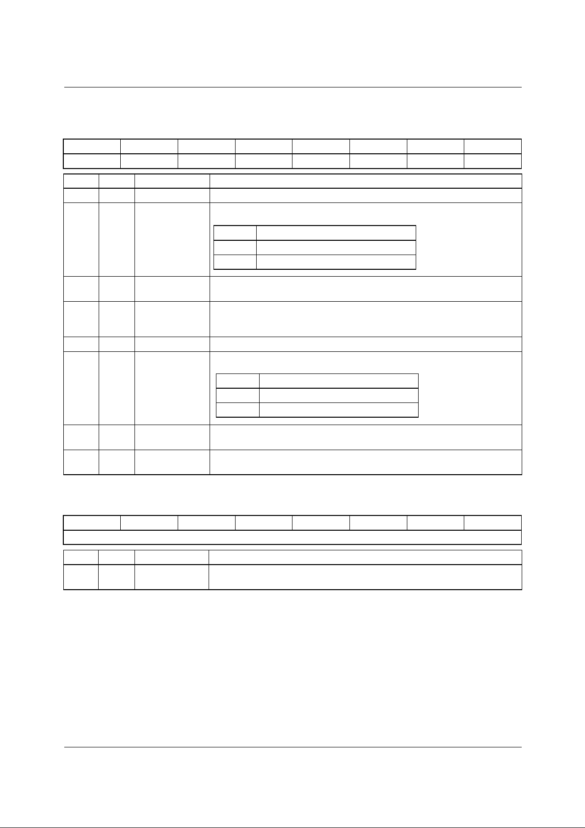
Chroma Processor Control (03)
76543210
BLFS CCEN CCOR GAUBY GAUSEL
Reg Bit Name Description
03 7-5 BLFS Burst loop filter select.
03 4 CCEN Chroma coring enable. Enables Chroma Coring when HIGH.
03 3-2 CCOR Chroma coring threshold. Sets the Chroma Coring threshold.
03 1 GAUBY Gaussian filter bypass. The chroma data bypasses the Gaussian LPF when
HIGH.
03 0 GAUSEL Gaussian LPF select. Selects the Gaussian filter response to be used on the
demodulated chrominance.
See Figure 22 for filter responses.
BLFS fS (Mpps) Recommended Criteria
000 13.5 PAL, Line-Locked YC
000 15 PAL, Line-Locked YC
001 12.27 NTSC, Line-Locked YC
001 13.5 PAL, Line-Locked Composite
010 13.5 NTSC, Line-Locked YC
010 15 PAL, Line-Locked Composite
011 14.32 NTSC, Subcarrier-Locked YC
011 17.73 PAL, Subcarrier-Locked Composite
100 17.73 PAL, Subcarrier-Locked YC
101 13.5 NTSC, Line-Locked Composite
110 12.27 NTSC, Line-Locked Composite
111 14.32 NTSC, Subcarrier-Locked Composite
CCOR Function
00 1 lsb
01 2 lsb
10 3 lsb
11 4 lsb
GAUSEL Function
0 Select Gaussian LPF resp. 2
1 Select Gaussian LPF resp. 1
Page 15
PRODUCT SPECIFICATION TMC22x5yA
REV. 1.0.0 2/4/03 15
Control Register Definitions (continued)
Burst Threshold (04)
76543210
BTH
Reg Bit Name Description
04 7-0 BTH Burst threshold. The 8 bit value to be compared against the demodulated
U and V component data. If over 127 lines occur in a field in which the burst
is below this threshold, then the color is set to chroma black for the next field.
Pedestal (05)
76543210
PED
Reg Bit Name Description
05 7-0 PED Pedestal level. An 8 bit magnitude subtracted from the luma data to remove
the setup before processing by the output matrix.
Luma Processor Control (06)
76543210
Reserved ANEN ANR ANT YSEL NOTCH
Reg Bit Name Description
06 7-6 Reserved Reserved, set to zero.
06 5 ANEN Adaptive notch enable. Enables adaptive notch when HIGH.
06 4 ANR Adaptive notch rounding. Sets adaptive notch rounding point.
06 3-2 ANT Adaptive notch threshold level. Sets the adaptive notch threshold.
06 1 YSEL Adaptive notch select. Selects adaptive notch filter response.
06 0 NOTCH Notch enable. Adaptive notch filter ANF3 selected when HIGH and ANEN is
HIGH, non-adaptive notch filter selected when HIGH and ANEN is LOW.
Function may be overridden by XSF (Reg 0E, bits 5-4).
ANR Function
0 Round to 10 bits
1 Round to 8 bits
ANT Function
00 Magnitude difference less than 32
01 Magnitude difference less than 24
10 Magnitude difference less than 16
11 Magnitude difference less than 8
YSEL Function
0 Adaptive notch response ANF1
1 Adaptive notch response ANF2
Page 16
TMC22x5yA PRODUCT SPECIFICATION
16 REV. 1.0.0 2/4/03
Control Register Definitions (continued)
Comb Processor Control (07)
76543210
LS1BY LS1IN LS2DLY SPLIT BSFBY BSFSEL BSFMSB GRSDLY
Reg Bit Name Description
07 7 LS1BY Line store 1 bypass. Bypasses linestore 1 when HIGH.
07 6 LS1IN Line store 1 input. Selects the input of linestore 1:
07 5 LS2DLY Line store 2 delay. LSTORE2 uses STS to store 1H when LOW and uses
VL to store SAV to EAV (or max count) when HIGH.
07 4 SPLIT Line store 2 delay. Splits data through LSTORE2, 9 bits chroma and 7 bits
luma when HIGH (chroma combs) and 8 bits chroma and 8 bits luma when
LOW (luma comb).
07 3 BSFBY Bandsplit filter bypass. Bandsplit filter is bypassed when HIGH.
07 2 BSFSEL Bandsplit filter select. Selects the bandsplit filter to be used:
07 1 BSFMSB Inverts msb of bandsplit filter. When HIGH, inverts the msb of the input to
the bandsplit filter.
07 0 GRSDLY Delays input to GRS decode. When HIGH, delays the input to the GRS
extraction circuit by 1H. Genlock only.
Mid-Sync Level (08)
76543210
MIDS
Reg Bit Name Description
08 7-0 MIDS Mid sync level. Sets the mid point of syncs for the mixed sync separator, in
the subcarrier locked mode.
LS1IN Function
0 Primary Input
1 Secondary Input
BSFSEL Function
0 Select bandsplit filter response 1
1 Select bandsplit filter response 2
Page 17
PRODUCT SPECIFICATION TMC22x5yA
REV. 1.0.0 2/4/03 17
Control Register Definitions (continued)
Extended DRS (09)
76543210
PCKF VSTD
Reg Bit Name Description
09 7-4 PCKF Clock rate.
09 3-0 VSTD Video Standard. Selects the video standard.
PCKF Function
0000 13.50 MHz
0001 reserved
0010 reserved
0011 reserved
0100 14.32 MHz
0101 17.73 MHz
0110 reserved
0111 reserved
1000 12.27 MHz
1001 14.75 MHz
1010 15.00 MHz
1011 reserved
1100 reserved
1101 reserved
1110 reserved
1111 reserved
VSTD Function
0000 NTSC-M
0001 NTSC-EIAJ
0010 reserved
0011 reserved
0100 reserved
0101 reserved
0110 reserved
0111 reserved
1000 PAL-B, G, H, I
1001 PAL-M
1010 PAL-N (Argentina, Paraguay, Uruguay)
1011 PAL-N (Jamaica)
1100 reserved
1101 reserved
1110 reserved
1111 reserved
Page 18
TMC22x5yA PRODUCT SPECIFICATION
18 REV. 1.0.0 2/4/03
Control Register Definitions (continued)
Notes:
1. To enable “super blacks” and disable syncs of the output simply set MSEN[1] HIGH and the sync gain to zero.
Output Control (0A)
76543210
OP8B OPLMT OPLMT MSEN OPCMSB YBAL BUREN
Reg Bit Name Description
0A 7 OP8B Output rounded to 8 bits. Rounds the outputs to 8 bits when HIGH. The two
lsbs are set to zero.
0A 6-5 OPLMT Output limit select. Sets the output format and limiters:
0A 4-3 MSEN Mixed sync enable. Sets composite sync output format:
0A 2 OPCMSB Chroma output msb invert. Inverts the msb of the C
BCR
or Chroma output
when HIGH.
0A 1 YBAL Luma color correction. Setting this bit HIGH forces the chroma to zero
whenever the luma equals or exceeds the luma limit.
0A 0 BUREN Output burst enable. When HIGH, passes the burst through on the chroma
channel. Sets the burst region to zero when LOW.
OPLMT Function
00 RGB output format
limited to 4 to 1016
01 YCBCR output format
Y limited to 4 to 1016
CBCR limited to ±504
10 RGB output format
limited to 4 to 1016
11 YCBCR output format
Y limited to 64 to 940
CBCR limited to ±448
MSEN Function
00 No sync, & “super blacks” disabled
01 No sync, & “super blacks” disabled
10 Sync on G/Y output only, & “super blacks” enabled
11 Sync on RGB outputs, & “super blacks” enabled
Page 19
PRODUCT SPECIFICATION TMC22x5yA
REV. 1.0.0 2/4/03 19
Control Register Definitions (continued)
Output Control (0B)
76543210
FMT422 CDEC YUVT Reserved DRSEN DRSCK
Reg Bit Name Description
0B 7 FMT422 Enables C
BCR
output mux. When HIGH, multiplexes the CB and CR data
onto the same data bus. The chroma or multiplexed C
BCR
output appears on
the B/C
B
output. The R/CR output is forced low.
0B 6 CDEC C
BCR
decimation enable. When HIGH, the CBCR data are decimated to
0:2:2 in the output processor.
0B 5 YUVT Enables D1 output. When HIGH, enables 4:2:2 multiplexed YC
BCR
onto the
R/CR data output with TRS words inserted into the output data stream. The Y
data are still available on the G/Y output and multiplexed CBCR is available on
the B/U output.
0B 4-2 Reserved Reserved, set to zero.
0B 1 DRSEN DRS output enable. When HIGH, enables the DRS onto the G/Y output.
0B 0 DRSCK DRS data rate. Sets the DRS output data rate.
DRSCK Function
0 Embeds data bytes (8 bits) at PCK
clock rate
1 Embeds data nibbles (4 bits) at
PXCK clock rate
Page 20
TMC22x5yA PRODUCT SPECIFICATION
20 REV. 1.0.0 2/4/03
Control Register Definitions (continued)
Comb Filter Control (0C)
76543210
ADAPT YCES YCSEL COMB
Reg Bit Name Description
0C 7-6 ADAPT Adaption mode. Sets the 3-line comb filter adaption mode in NTSC.
0C 5 YCES YC input error signal control. Error signal control for YC input, luma comb.
0C 4 YCSEL Luma/chroma comb filter select. Selects luma or chroma comb filter.
0C 3-0 COMB Comb filter architecture.
ADAPT[1:0] Function
00 Adapts to best of 3 types of line based comb filters in NTSC
only.
01 Adapts to the best of two field or frame based comb filters
in NTSC only.
10 3 line (tap) comb only. Never adapts to a 2 line (tap) filter.
The higher set of comb filter error signals are sent to the
XLUT. NTSC or PAL comb filter.
11 Adapts to best of two 3 line chroma comb filters in PAL only.
YCES Function
0 LPF and HPF error signal, between (0H & 1H) or (1H & 2H) in
NTSC or between (0H & 2H) in PAL,are sent to XLUT
1 LPF error signal, between (0H & 1H) and (1H & 2H) in NTSC or
between (0H & 2H) in PAL, are sent to XLUT
YCSEL Function
0 Chroma comb filter
1 Luma comb filter
COMB Function
YC or composite comb filter architectures
0000 PAL or NTSC 3 line comb
0001 NTSC 3 line comb (0H & 1H)
0010 NTSC 3 line comb (1H & 2H)
0011 NTSC 2 line comb (0H & 1H)
0100 NTSC (2 line) field comb
0101 NTSC or PAL field comb
0110 NTSC (2 line) frame comb
0111 NTSC frame comb
D1 comb filter architectures
1000 3 line comb
1001 3 line comb (0H & 1H)
1010 3 line comb (1H & 2H)
1011 3 line comb (0H & 2H)
1100 (2 line) field comb
1101 field or 2 line (0H & 1H) comb
1110 (2 line) frame comb
1111 frame comb
Page 21
PRODUCT SPECIFICATION TMC22x5yA
REV. 1.0.0 2/4/03 21
Control Register Definitions (continued)
Comb Filter Control (0D)
76543210
CEST CESG YESG CESTBY XFEN FAST YWBY
Reg Bit Name Description
0D 7-6 CEST Chroma error signal transform.
0D 5 CESG Chroma error signal gain.
0D 4 YESG Luma error signal gain.
0D 3 CESTBY Chroma error signal bypass. When HIGH, bypasses chroma error signal.
0D 2 XFEN XLUT filter enable. When HIGH, enables the LPF on the XLUT output.
0D 1 FAST Adaption speed select. When HIGH, the 3 line comb filter selects between
comb filter architectures on a pixel by pixel basis. When LOW, the selection
is filtered.
0D 0 YWBY Luma weighting bypass. When HIGH bypasses the luma fail weighting.
CEST Video Standard Clock Rate (MHz)
00 PAL/NTSC 4*Fsc & 13.5MHz
01 NTSC 12.27MHz
10 PAL 14.75MHz
11 PAL 15MHz
CESG Function
0 Normal chroma fail signal levels
1 Double the chroma error signal levels
YESG Function
0 Normal luma fail signal levels
1 Double the luma error signal levels
Page 22
TMC22x5yA PRODUCT SPECIFICATION
22 REV. 1.0.0 2/4/03
Control Register Definitions (continued)
Comb Filter Control (0E)
76543210
XIP XSF YMUX CMUX
Reg Bit Name Description
0E 7-6 XIP XLUT input select. Selects the comb fail signals presented to the XLUT:
0E 5-4 XSF XLUT special function.
0E 3-2 YMUX Y output select. Output selection of luma 4:1 mux
0E 1-0 CMUX C output select. Output selection of chroma 4:1 mux
XIP[1:0] Input to XLUT
00 2 bits of phase error (X[7:6]), 3 bits of chroma
(X[5:3]) and luma magnitude error (X[3:0]).
01 4 bits of chroma (X[7:4]) and luma magnitude
error (X[3:0]).
10 3 bits of phase error (X[7:5]), 3 bits of chroma
magnitude error (X[4:2]), and 2 bits of luma
magnitude error (X[1:0]).
11 4 bits of phase error (X[7:4]) and chroma
magnitude error (X[3:0]).
XSF Luma Chroma
00 Comb Simple
01 Simple Comb
10 Flat with notch Simple
11 Flat with notch Comb
YMUX Output
00 Comb
01 Flat - Comb
10 Flat
11 Simple
CMUX Output
00 Comb
01 Flat - Comb
10 Flat
11 Simple
Page 23
PRODUCT SPECIFICATION TMC22x5yA
REV. 1.0.0 2/4/03 23
Control Register Definitions (continued)
Comb Filter Control (0F)
76543210
Reserved CAT DCES IPCF YCCOMP SYNC
Reg Bit Name Description
0F 7 Reserved Reserved, set to zero.
0F 6-5 CAT Adaption threshold. Fixes threshold at which different comb filters are selected.
0F 4 DCES D1 C
BCR
error signal. When set LOW for D1 chroma comb filters:
a) In 3 line comb filter architectures, the magnitude error between the component
data for that pixel selects the 3 line comb or adapts to a
2 line comb. On a “CB pixel” the error signal selected on pixel (x+4) is sent to
the XLUT with the magnitude difference between “CR pixels” on the same pair
of lines, but from pixel (x+3). Likewise on a “CR pixel” the error signal selected
on pixel (x+5) is sent to the XLUT with the magnitude difference between “CB
pixels” on the same lines but from pixel (x+4).
b) In 2 line comb filters the magnitude differences between the same pair of lines
is always sent to the XLUT, On a “CB pixel” the error from the preceding “CR
pixel” is used and on a “CR pixel” the preceding “CB pixel” would be used.
When set HIGH for D1 chroma filters:
This is used for 3 line comb filter architecture that are inhibited from adapting to 2
line comb filter architectures. The input to the XLUT is the magnitude error in C
R
between (0H & 1H) and (1H & 2H) on “CR pixels” and the magnitude error
between (0H & 1H) and (1H & 2H) on “CB pixels”.
0F 3-2 IPCF Comb filter input select. Selects primary inputs to the comb filter.
0F 1 YCCOMP YC or Composite input select. Selects YC inputs when HIGH and composite
inputs when LOW.
0F 0 SYNC Sync processor select. The syncs are obtained by a LPF when HIGH and by the
comb filter when LOW.
Sync Pulse Generator (10)
76543210
STS
7
STS
6
STS
5
STS
4
STS
3
STS
2
STS
1
STS
0
Reg Bit Name Description
10 7-0 STS
7-0
Sync to sync 8 lsbs. Bottom 8 bits of the number of pixels between sync
pulses.
0
0
1
1
0
1
0
1
5% of max error
15% of max error
25% of max error
50% of max error
IPCF Function
0 0
0 1
1 0
1 1
Flat video
LPF output
HPF output
Reserved
Page 24
TMC22x5yA PRODUCT SPECIFICATION
24 REV. 1.0.0 2/4/03
Control Register Definitions (continued)
Sync Pulse Generator (11)
76543210
STB
Reg Bit Name Description
11 7-0 STB Sync to burst. Controls the number of pixels from sync to burst. This signal
starts the burst sample and hold. In SC mode, subtract 25 from the desired
delay to generate this value.
Sync Pulse Generator (12)
76543210
BTV
Reg Bit Name Description
12 7-0 BTV Burst to video. Controls the number of pixels from STB to the start of active
video.
Sync Pulse Generator (13)
76543210
AV
7
AV
6
AV
5
AV
4
AV
3
AV
2
AV
1
AV
0
Reg Bit Name Description
13 7-0 AV
7-0
Active video line 8 lsbs. Bottom 8 bits of the number of pixels during the
active video line.
Sync Pulse Generator (14)
76543210
Reserved AV
9
AV
8
Reserved STS
10
STS
9
STS
8
Reg Bit Name Description
14 7-6 Reserved Reserved, set to zero.
14 5-4 AV
9-8
Active video line 2 msbs. Two most significant bits of AV.
14 3 Reserved Reserved, set to zero.
14 2-0 STS
10-8
Sync to sync 3 msbs. Three most significant bits of STS.
Page 25
PRODUCT SPECIFICATION TMC22x5yA
REV. 1.0.0 2/4/03 25
Control Register Definitions (continued)
Sync Pulse Generator (15)
76543210
Reserved VINDO VDIV VDOV
Reg Bit Name Description
15 7 Reserved Reserved, set to zero.
15 6-2 VINDO Number of lines in vertical window. The number of lines (0 to 31) after the
last EQ pulse that the decoder passes through the Vertical INterval winDOw.
15 1 VDIV Action inside VINDO. The vertical data inside the `VINDO' is passed
through a simple decoder when LOW, or is passed unprocessed on the luma
channel with the chroma channel set to zero when HIGH.
15 0 VDOV Action outside VINDO. The vertical data after the `VINDO' and before the
end of vertical blanking is blanked (YUV = 0) when LOW, or passed through
the simple decoder when HIGH.
Sync Pulse Generator (16)
76543210
Reserved NFDLY SPGIP MSIP
Reg Bit Name Description
16 7-6 Reserved Reserved, set to zero.
16 5-4 NFDLY new field detect delay. NTSC frame detect delay:
16 3-2 SPGIP SPG input select. Selects the input to the Sync Pulse Generator:
16 1 MSIP Mixed sync separator input. Set HIGH for external VIDEOB reference or
LOW for output of Low Pass Filter.
16 0 SMO State Machine Offset. Set HIGH for a 1H offset and LOW for a 0H offset.
NFDLY Function
00 pixel count = 0
01 pixel count = 1
10 pixel count = 2
11 pixel count = 3
SPGIP Input
00 External HSYNC and VSYNC
01 Digitized sync (subcarrier mode)
10 TRS words embedded in the D1 data stream
11 TRS words embedded in the D2 data stream
Page 26
TMC22x5yA PRODUCT SPECIFICATION
26 REV. 1.0.0 2/4/03
Control Register Definitions (continued)
Buffered register set 0 (17) Active when BUFFER pin set LOW.
76543210
SG0
7
SG0
6
SG0
5
SG0
4
SG0
3
SG0
2
SG0
1
SG0
0
Reg Bit Name Description
17 7-0 SG0
7-0
Msync gain, 8 lsbs. Bottom 8 bits of mixed sync scalar
lsb = 1/256
Buffered register set 0 (18) Active when BUFFER pin set LOW.
76543210
YG0
7
YG0
6
YG0
5
YG0
4
YG0
3
YG0
2
YG0
1
YG0
0
Reg Bit Name Description
18 7-0 YG0
7-0
Y gain, 8 lsbs. Bottom 8 bits of the luma gain
lsb = 1/256
Buffered register set 0 (19) Active when BUFFER pin set LOW.
76543210
UG0
7
UG0
6
UG0
5
UG0
4
UG0
3
UG0
2
UG0
1
UG0
0
Reg Bit Name Description
19 7-0 UG0
7-0
U gain, 8 lsbs. Bottom 8 bits of the U gain
lsb = 1/256
Buffered register set 0 (1A) Active when BUFFER pin set LOW.
76543210
VG0
7
VG0
6
VG0
5
VG0
4
VG0
3
VG0
2
VG0
1
VG0
0
Reg Bit Name Description
1A 7-0 VG0
7-0
V gain, 8 lsbs. Bottom 8 bits of the V gain
lsb = 1/256
Buffered register set 0 (1B) Active when BUFFER pin set LOW.
76543210
YG0
9
YG0
8
UG0
10
UG0
9
UG0
8
Reserved VG0
9
VG0
8
Reg Bit Name Description
1B 7-6 YG0
9-8
Y gain, 2 msb. Top 2 bits of the Y gain. msb = 2
1B 5-3 UG0
10-8
U gain, 3 msbs. Top 3 bits of the U gain. msb = 4
1B 2 Reserved Reserved, set to zero.
1B 1-0 VG0
9-8
V gain, 2 msbs. Top 2 bits of the V gain. msb = 2
Page 27

PRODUCT SPECIFICATION TMC22x5yA
REV. 1.0.0 2/4/03 27
Control Register Definitions (continued)
Buffered register set 0 (1C) Active when BUFFER pin set LOW.
76543210
YOFF0
7
YOFF0
6
YOFF0
5
YOFF0
4
YOFF0
3
YOFF0
2
YOFF0
1
YOFF0
0
Reg Bit Name Description
1C 7-0 YOFF0
7-0
Y offset, 8 lsbs. Bottom 8 bits of luma or RGB offset
Buffered register set 0 (1D) Active when BUFFER pin set LOW.
76543210
Reserved YOFF0
8
SG0
9
SG0
8
Reg Bit Name Description
1D 7-3 Reserved Reserved, set to zero.
1D 2 YOFF0
8
Y offset, msb. msb of YOFF
1D 1-0 SG0
9-8
Msync gain, 2 msbs. Top 2 bits of mixed sync scalar.
msb = 2
Buffered register set 0 (1E) Active when BUFFER pin set LOW.
76543210
SYSPH0
6
SYSPH0
5
SYSPH0
4
SYSPH0
3
SYSPH0
2
SYSPH0
1
SYSPH0
0
VAXIS0
Reg Bit Name Description
1E 7-1 SYSPH0
6-0
7 lsbs of phase offset. Bottom 7 bits of the 15 bit system phase offset
1E 0 VAXIS0 V axis flip. Flips the sign of the V axis when HIGH.
Buffered register set 0 (1F) Active when BUFFER pin set LOW.
76543210
SYSPH0
14
SYSPH0
13
SYSPH0
12
SYSPH0
11
SYSPH0
10
SYSPH0
9
SYSPH0
8
SYSPH0
7
Reg Bit Name Description
1F 7-0 SYSPH0
14-7
8 msbs of phase offset. Top 8 bits of 15 bit system phase offset.
Normalized Subcarrier Frequency (20)
76543210
FSC
3
FSC
2
FSC
1
FSC
0
Reserved
Reg Bit Name Description
20 7-4 FSC
3-0
Bottom 4 bits of fsc. Bottom 4 bits of the 28 bit subcarrier SEED
20 3-0 Reserved Reserved, set to zero.
Page 28

TMC22x5yA PRODUCT SPECIFICATION
28 REV. 1.0.0 2/4/03
Control Register Definitions (continued)
Normalized Subcarrier Frequency (21)
76543210
FSC
11
FSC
10
FSC
9
FSC
8
FSC
7
FSC
6
FSC
5
FSC
4
Reg Bit Name Description
21 7-0 FSC
11-4
Lower 8 bits of fsc. Lower 8 bits of the 28 bit subcarrier SEED
Normalized Subcarrier Frequency (22)
76543210
FSC
19
FSC
18
FSC
17
FSC
16
FSC
15
FSC
14
FSC
13
FSC
12
Reg Bit Name Description
22 7-0 FSC
19-12
Middle 8 bits of fsc. Middle 8 bits of the 28 bit subcarrier SEED
Normalized Subcarrier Frequency (23)
76543210
FSC
27
FSC
26
FSC
25
FSC
24
FSC
23
FSC
22
FSC
21
FSC
20
Reg Bit Name Description
23 7-0 FSC
27-20
Top 8 bits of fsc. Top 8 bits of the 28 bit subcarrier SEED
Page 29

PRODUCT SPECIFICATION TMC22x5yA
REV. 1.0.0 2/4/03 29
Control Register Definitions (continued)
Normalized Subcarrier Frequency (24)
76543210
CLMPEN PFLTEN CLPSEL
1-0
CLPBY CLPOF
2-0
Reg Bit Name Description
24 7 DREFSEL Decoder Reference Signal Select. When HIGH, enables a negative going
clamp pulse on the DREF pin. The position of the clamp pulse is controlled
by register 24. When LOW the DREF pin is HIGH during the active video
portion of each line and LOW during the horizontal and vertical blanking
intervals.
24 6 PFLTBY Phase error filter bypass. When HIGH, no filtering is done on the phase
error signals for the comb filter adapter. When LOW, the filter is enabled.
24 5-4 CLPSEL
1-0
Internal black level clamp selection.
24 3 VCLPEN Vertical clamp filter enable. When LOW, vertical clamp filter is disabled.
When HIGH, vertical clamp filter is enabled.
24 2-0 BAND
2-0
Clamp guard band. When an error value between two consecutive lines
black level is less than the guard band, it does not effect the filtered black
level.
Normalized Subcarrier Frequency (25)
76543210
CPDLY
7-0
Reg Bit Name Description
25 7-0 CPDLY
7-0
Clamp pulse delay. Controls the number of clock cycles from hsync before
the 0.5 µSec clamp pulse is output to the AVOUT pin. This option is only
enabled when register 24 bit 7 is set HIGH.
CLMP[1:0] Function
00 Clamp disabled, black level set to 240
01 Clamp disabled, black level set to 256
10 Clamp enabled, use Delayed VIDEOB input as
reference
11 Clamp enabled, use LPF as reference
BANDS[2:0] Function
000 No guard band
001 error value < 2
010 error value < 4
011 error value < 6
100 error value < 8
101 error value < 10
110 error value < 12
111 error value < 15
Page 30

TMC22x5yA PRODUCT SPECIFICATION
30 REV. 1.0.0 2/4/03
Control Register Definitions (continued)
Output Format Control (26)
76543210
Reserved LDVIO OPCKS DPCEN DPC
Reg Bit Name Description
26 7-6 Reserved Reserved, set to zero.
26 5 LDVIO LDV clock select. LDV is an output when LOW and an input when HIGH
26 4 OPCKS Output clock select. The output data are clocked by the CLOCK pin when
LOW and by the LDV pin when HIGH.
26 3 DPCEN DPC enable. When HIGH on the TMC22153A, the Decoder Product Code is
enabled: a value written into DPC determines the decoder product emulated
by the TMC22153A. In all other versions of the decoder, DPC is read-only,
and returns the code of the particular encoder version installed.
26 2-0 DPC Decoder product code
Read/Write in the TMC22153A only. Read-only in all other devices.
Buffered register set 1 (27) Active when BUFFER pin set HIGH.
76543210
SG1
7
SG1
6
SG1
5
SG1
4
SG1
3
SG1
2
SG1
1
SG1
0
Reg Bit Name Description
27 7-0 SG1
7-0
Msync gain, 8 lsbs. Bottom 8 bits of the mixed sync scalar
lsb = 1/256
Buffered register set 1 (28) Active when BUFFER pin set HIGH.
76543210
YG1
7
YG1
6
YG1
5
YG1
4
YG1
3
YG1
2
YG1
1
YG1
0
Reg Bit Name Description
28 7-0 YG1
7-0
Y gain, 8 lsbs. Bottom 8 bits of the luma gain
lsb = 1/256
DPC Function
000 Reserved
001 TMC22051A
010 TMC22052A
011 TMC22053A
100 Reserved
101 TMC22151A
110 TMC22152A
111 TMC22153A
Page 31

PRODUCT SPECIFICATION TMC22x5yA
REV. 1.0.0 2/4/03 31
Control Register Definitions (continued)
Buffered register set 1 (29) Active when BUFFER pin set HIGH.
76543210
UG1
7
UG1
6
UG1
5
UG1
4
UG1
3
UG1
2
UG1
1
UG1
0
Reg Bit Name Description
29 7-0 UG1
7-0
U gain, 8 lsbs. Bottom 8 bits of the U gain
lsb = 1/256
Buffered register set 1 (2A) Active when BUFFER pin set HIGH.
76543210
VG1
7
VG1
6
VG1
5
VG1
4
VG1
3
VG1
2
VG1
1
VG1
0
Reg Bit Name Description
2A 7-0 VG1
7-0
V gain, 8 lsbs. Bottom 8 bits of the V gain
lsb = 1/256
Buffered register set 1 (2B) Active when BUFFER pin set HIGH.
76543210
YG1
9
YG1
8
UG1
10
UG1
9
UG1
8
Reserved VG1
9
VG1
8
Reg Bit Name Description
2B 7-6 YG1
9-8
Y gain, 2 msbs. Top 2 bits of the Y gain
msb = 2
2B 5-3 UG1
10-8
U gain, 3 msbs. Top 3 bits of the U gain.
msb = 4
2B 2 Reserved reserved, set to zero
2B 1-0 VG1
9-8
V gain, 2 msbs. Top 2 bits of the V gain
msb = 2
Buffered register set 1 (2C) Active when BUFFER pin set HIGH.
76543210
YOFF1
7
YOFF1
6
YOFF1
5
YOFF1
4
YOFF1
3
YOFF1
2
YOFF1
1
YOFF1
0
Reg Bit Name Description
2C 7-0 YOFF1
7-0
Y offset, 8 lsbs. Bottom 8 bits of luma or RGB offset
Page 32

TMC22x5yA PRODUCT SPECIFICATION
32 REV. 1.0.0 2/4/03
Control Register Definitions (continued)
Buffered register set 1 (2D) Active when BUFFER pin set HIGH.
76543210
Reserved YOFF1
8
SG1
9
SG1
8
Reg Bit Name Description
2D 7-3 Reserved Reserved, set to zero.
2D 2 YOFF1
8
Y offset, msb. msb of YOFF
2D 1-0 SG1
9,8
Msync gain, 2 msbs. Top 2 bits of mixed sync scalar
msb = 2
Buffered register set 1 (2E) Active when BUFFER pin set HIGH.
76543210
SYSPH1
6
SYSPH1
5
SYSPH1
4
SYSPH1
3
SYSPH1
2
SYSPH1
1
SYSPH1
0
VAXISO
Reg Bit Name Description
2E 7-1 SYSPH1
6-0
7 lsbs of phase offset. Bottom 7 bits of the 15 bit system phase offset
2E 0 VAXIS1 V axis flip. Flips the sign of the V axis when HIGH.
Buffered register set 1 (2F) Active when BUFFER pin set HIGH.
76543210
SYSPH1
14
SYSPH1
13
SYSPH1
12
SYSPH1
11
SYSPH1
10
SYSPH1
9
SYSPH1
8
SYSPH1
7
Reg Bit Name Description
2F 7-0 SYSPH1
14-7
8 msbs of phase offset. Top 8 bits of 15 bit system phase offset.
Page 33

PRODUCT SPECIFICATION TMC22x5yA
REV. 1.0.0 2/4/03 33
Control Register Definitions (continued)
Video Measurement (30)
76543210
Reserved LGF LGEN LGEXT RESERVED PGG PGEN PGEXT
Reg Bit Name Description
30 7 Reserved Reserved, set to zero.
30 6 LGF Line grab flag. Set HIGH when the decoder has grabbed a line, and must be
reset LOW before another line can be grabbed.
30 5 LGEN Line grab enable. When HIGH, the line grabber is used to freeze the
contents of the line store, at the programmed line and field count. The phase
and frequency of the frozen line are also stored from the DRS, and are
continually used to reset the DDS, once per line, until LGF is set LOW. When
LGEN is LOW, the line freeze is disabled, the internal loops operate normally,
and the line grab signal is used only to gate the pixel grab.
30 4 LGEXT Ext line grab enable. The SET pin is used to produce the line grabber pulse
when HIGH and the internal line decode is used when LGEXT is LOW.
30 3 Reserved Reserved, set to zero.
30 2 PGG Pixel grab gate. When HIGH the pixel grab is gated by the field and line grab
signals to enable one pixel per four fields in NTSC and 8 field in PAL to be
grabbed. This function is disabled if PGEN is set LOW.
30 1 PGEN Pixel grab enable. When HIGH the 10 bit G/Y, B/U, and R/V data, and the
mixed sync and luma data after the comb filter, and the demodulated (B-Y)
and (R-Y) color difference signals are grabbed once every line at the
programmed pixel grab number. When LOW the contents of the pixel grab
registers are held and the pixel grab pulse is ignored.
30 0 PGEXT Ext pixel grab enable. The SET pin is used to produce the pixel grab pulse
when HIGH and the internal pixel decode is used when PGEXT is LOW.
Video Measurement (31)
76543210
PG
7
PG
6
PG
5
PG
4
PG
3
PG
2
PG
1
PG
0
Reg Bit Name Description
31 7-0 PG
7-0
Pixel grab, 8 lsbs. Bottom 8 bits of the pixel grab.
Video Measurement (32)
76543210
LG
7
LG
6
LG
5
LG
4
LG
3
LG
2
LG
1
LG
0
Reg Bit Name Description
32 7-0 LG
7-0
Line grab, 8 lsbs. Bottom 8 bits of the line grab.
Page 34

TMC22x5yA PRODUCT SPECIFICATION
34 REV. 1.0.0 2/4/03
Control Register Definitions (continued)
Registers 34-3C are Read-Only
Video Measurement (33)
76543210
Reserved FG LG
8
PG
10
PG
9
PG
8
Reg Bit Name Description
33 7 Reserved Reserved.
33 6-4 FG Field grab number. Field grab number
33 3 LG
8
Msb of line grab. msb of line grab
33 2-0 PG
10-8
Pixel grab, 3 msbs. 3 msbs of pixel grab
Register (34)
76543210
GY
9
GY
8
GY
7
GY
6
GY
5
GY
4
GY
3
GY
2
Reg Bit Name Description
34 7-0 GY
9-2
G/Y grab, 8 msbs. Top 8 bits of the "grabbed" G/Y data
Register (35)
76543210
BU
9
BU
8
BU
7
BU
6
BU
5
BU
4
BU
3
BU
2
Reg Bit Name Description
35 7-0 BU
9-2
B/U grab, 8 msbs. Top 8 bits of the "grabbed" B/U data
Register (36)
76543210
RV
9
RV
8
RV
7
RV
6
RV
5
RV
4
RV
3
RV
2
Reg Bit Name Description
36 7-0 RV
9-2
R/V grab, 8 msbs. Top 8 bits of the "grabbed" R/V data
Register (37)
76543210
Reserved GY
1
GY
0
BU
1
BU
0
RV
1
RV
0
Reg Bit Name Description
37 7-6 Reserved Reserved.
37 5-4 GY
1-0
G/Y grab, 2 lsbs. Bottom two bits of G/Y data
37 3-2 BU
1-0
B/U grab, 2 lsbs. Bottom two bits of B/U data
37 1-0 RV
1-0
R/V grab, 2 lsbs. Bottom two bits of R/V data
Page 35

PRODUCT SPECIFICATION TMC22x5yA
REV. 1.0.0 2/4/03 35
Control Register Definitions (continued)
Register
(38)
76543210
Y
9
Y
8
Y
7
Y
6
Y
5
Y
4
Y
3
Y
2
Reg Bit Name Description
38 7-0 Y
9-2
Luma grab, 8 msbs. Top 8 bits of the "grabbed" luma data after YPROC
Register (39)
76543210
M
9
M
8
M
7
M
6
M
5
M
4
M
3
M
2
Reg Bit Name Description
39 7-0 M
9-2
Msync grab, 8 msbs. Top 8 bits of the "grabbed" mixed sync data after
YPROC
Register (3A)
76543210
U
9
U
8
U
7
U
6
U
5
U
4
U
3
U
2
Reg Bit Name Description
3A 7-0 U
9-2
U grab, 8 msbs. Top 8 bits of the "grabbed" U data
Register (3B)
76543210
V
9
V
8
V
7
V
6
V
5
V
4
V
3
V
2
Reg Bit Name Description
3B 7-0 V
9-2
V grab, 8 msbs. Top 8 bits of the "grabbed" V data
Register (3C)
76543210
Y
1
Y
0
M
1
M
0
U
1
U
0
V
1
V
0
Reg Bit Name Description
3C 7-6 Y
1-0
Luma grab, 2 lsbs. Bottom 2 bits of luma data
3C 5-4 M
1-0
Msync grab, 2 lsbs. Bottom 2 bits of mixed sync data
3C 3-2 U
1-0
U grab, 2 lsbs. Bottom 2 bits of U data
3C 1-0 V
1-0
V grab, 2 lsbs. Bottom 2 bits of V data
Page 36

TMC22x5yA PRODUCT SPECIFICATION
36 REV. 1.0.0 2/4/03
Control Register Definitions (continued)
Test Control (3D-3E)
76543210
TEST
Reg Bit Name Description
3D-3E 7-0 TEST Must be set to zero. Auto increment stops at 3F
Test Control (3F)
76543210
VBIT20 PEDDIS CCDEN
5
CCDEN
4
CCDEN
3
CCDEN
2
CCDEN
1
CCDEN
0
Reg Bit Name Description
3F 7 VBIT20 VBIT20 enable. When HIGH the V bit within embedded TRS words is
extended through line 20 for NTSC. When LOW, this V bit is HIGH up to line
16 for NTSC. The PAL operation is unaffected by this register bit.
3F 6 PEDDIS Pedestal disable. When HIGH, pedestal is not removed from lines with
LID = 00 to 06, lines 0 through 16
3F 5 CCDEN
5
Closed caption data enable 5. When HIGH, enables NTSC line 21 field 0
or PAL line 22 field 0 to be passed ‘FLAT’, through the decoder, on the
luminance channel and the pedestal removal will be disabled.
3F 4 CCDEN
4
Closed caption data enable 4. When HIGH, enables NTSC line 22 field 0
or PAL line 23 field 0 to be passed ‘FLAT’, through the decoder, on the
luminance channel and the pedestal removal will be disabled.
3F 3 CCDEN
3
Closed caption data enable 3. When HIGH, enables NTSC line 23 field 0
or PAL line 24 field 0 to be passed ‘FLAT’, through the decoder, on the
luminance channel and the pedestal removal will be disabled.
3F 2 CCDEN
2
Closed caption data enable 2. When HIGH, enables NTSC line 283 field 1
or PAL line 334 field 1 to be passed ‘FLAT’, through the decoder, on the
luminance channel and the pedestal removal will be disabled.
3F 1 CCDEN
1
Closed caption data enable 1. When HIGH, enables NTSC line 284 field 1
or PAL line 335 field 1 to be passed ‘FLAT’, through the decoder, on the
luminance channel and the pedestal removal will be disabled.
3F 0 CCDEN
0
Closed caption data enable 0. When HIGH, enables NTSC line 285 field 1
or PAL line 336 field 1 to be passed ‘FLAT’, through the decoder, on the
luminance channel and the pedestal removal will be disabled.
Status - Read Only (40)
76543210
DDSPH
Reg Bit Name Description
40 7-0 DDSPH DDS phase, 8 msbs. The top 8 bits of the sine data generated in the internal
DDS.
Page 37

PRODUCT SPECIFICATION TMC22x5yA
REV. 1.0.0 2/4/03 37
Control Register Definitions (continued)
Status - Read Only (41)
76543210
LINEST BGST VACT2 PALODD VFLY FGRAB LGRAB PGRAB
Reg Bit Name Description
41 7 LINEST Pixel count reset. Pixel count reset
41 6 BGST Start of burst gate. Start of burst gate
41 5 VACT2 Half line flag. Half line flag
41 4 PALODD PAL Ident. PAL Ident (low on NTSC lines)
41 3 VFLY Vertical count reset. Vertical count reset
41 2 FGRAB Field grab. Field grab
41 1 LGRAB Line grab. Line grab
41 0 PGRAB Pixel grab. Pixel grab
Status - Read Only (42)
76543210
FLD VBLK HBLK LID
Reg Bit Name Description
42 7 FLD Field flag (F in D1 output). Field flag (F in D1 output)
42 6 VBLK Vertical blanking (V in D1 output). Vertical blanking (V in D1 output)
42 5 HBLK Horizontal blanking (H in D1 output). Horizontal blanking (H in D1 output)
42 4-0 LID Line identification. Line identification
Status - Read Only (43)
76543210
YGO YGU UBO UBU VRO VRU Reserved
Reg Bit Name Description
43 7 YGO Y/G overflow. Y/G overflow
43 6 YGU Y/G underflow. Y/G underflow
43 5 UBO CB/B overflow. CB/B overflow
43 4 UBU CB/B underflow. CB/B underflow
43 3 VRO CR/R overflow. CR/R overflow
43 2 VRU CR/R underflow. CR/R underflow
43 1-0 Reserved Reserved.
Page 38

TMC22x5yA PRODUCT SPECIFICATION
38 REV. 1.0.0 2/4/03
Control Register Definitions (continued)
Status - Read Only (44)
76543210
MONO FPERR
Reg Bit Name Description
44 7 MONO Color kill flag. High when burst detected and LOW when monochrome
signal is detected.
44 6-0 FPERR Frequency/Phase error. Top 7 bits of the modulo two pi frequency or phase
error. Reported once per line.
Status - Read Only (45)
76543210
DRS
Reg Bit Name Description
45 7-0 DRS DRS signal. The 8-bit Decoder Reference Signal.
Status - Read Only (46)
76543210
PARTID
Reg Bit Name Description
46 7-0 PARTID Part family ID. Reads back the 8-bit part ID number. Read-only. Returns
CDh.
Status - Read Only (47)
76543210
REVID
Reg Bit Name Description
47 7-0 REVID Recoder revision number.
REVID TMC22x5y Revision TMC22x5yA Revision
05 F
06 G
10 A
11 B
Page 39

PRODUCT SPECIFICATION TMC22x5yA
REV. 1.0.0 2/4/03 39
Control Register Definitions (continued)
Status - Read Only (48-4A)
76543210
Reserved
Status - Read Only (4B)
76543210
PKILL CFSTAT XOP
Reg Bit Name Description
4B 7 PKILL
Phase kill from comb fail. Phase kill from comb fail.
4B 6-5 CFSTAT Comb filter status. Comb filter status.
4B 4-0 XOP XLUT output. XLUT output.
Status - Read Only (4C-FF)
76543210
Reserved
Reg Bit Name Description
4C-FF 7-0 Reserved Reserved.
CFSTAT STATUS
00 3 tap comb
01 3 tap [lower] comb
10 3-tap [upper] comb
11 2 tap comb
Page 40

TMC22x5yA PRODUCT SPECIFICATION
40 REV. 1.0.0 2/4/03
Decoder Introduction
All composite video decoders perform fundamentally the
same operation. The first stage is to separate the luminance
and chrominance. The second stage is to lock the internally
generated sine and cosine waveforms to the burst on the
decoded chrominance signal, demodulate, and then filter the
chrominance signal to produce the color difference signals.
The last stage either scales the luminance and color difference signals, or converts them into red, green, and blue
component video signals. These three stages are shown in
Figure 3.
The complete separation of composite video signals into
pure luminance (luma) and chrominance (chroma) signals is
practically impossible, especially when the input source
contains intraframe motion. Therefore, the luminance (luma)
signal will generally contain some high frequency chrominance, termed cross luma, and the chroma signal will
contains some of the high frequency luma signal, centered
around the subcarrier frequency, termed cross color.
The degree of cross luma and cross color is directly proportional to the filter used for the YC separation, the picture content, and the complexity of any post processing of the
decoded signals.
Figure 3. Fundamental Decoder Block Diagram
65-22x5y-44
YC Filter
Y
Y
U
VB
R
G
C
Composite
Chrominance
sin(wt)
cos(wt+φ)
Luminance
–
–
–
–
–
–
–
–
Matrix
Demodulation
Green
Red
Blue
Burst Locked
Loop
YC Separation
The relationship between the chrominance and luminance
bandwidths is shown for both PAL and NTSC in Figure 4,
wherein the shaded area denotes the part of the composite
video frequency spectrum shared by both the chrominance
and high frequency luminance signals.
The Luma Notch and Chroma Bandpass Technique for
YC Separation
The simplest method of separating these chrominance and
luminance signals, is to assume the chroma bandwidth is
limited to a few hundred kilohertz around the subcarrier
frequency. In this case a notch filter designed to remove just
these frequencies from the composite video frequency
spectrum provides the luma signal, while a bandpass filter
Figure 4. Comparison of the Frequency Spectrum of NTSC and PAL Composite Video Signals
Chrominance
Subcarrier
PAL NTSC
Chrominance
(& High Frequency
Luminance)
Chrominance
(& High Frequency
Luminance)
Sound Carrier
Center Frequency
Chrominance
Subcarrier
Sound Carrier
Center Frequency
Frequency (MHz) Frequency (MHz)
Amplitude
(dB)
Amplitude
(dB)
Luminance
112 23 34 4 4.556
-20
-3
0
-20
-3
0
Luminance
Page 41

PRODUCT SPECIFICATION TMC22x5yA
REV. 1.0.0 2/4/03 41
centered at the subcarrier frequency produces the chroma
signal. This simple technique works well in pictures containing large flat areas of color, however this is rarely the case.
If, as is generally true, the picture contains high frequency
luma and chroma transitions, for example herring bone suit
jackets, branches of trees, text, etc., cross color and cross
luma artifacts are evident.
The presence of cross color or cross luma is generally
acceptable when viewing the decoded picture on a monitor
from several feet, as would be the case in most homes on
commercial television sets. However, these artifacts become
increasingly difficult to process, or ignore, when the image is
to be compressed or manipulated. In these cases more
sophisticated methods of separating the luma and chroma
signals, such as frame, field, or line based comb filter decoders, are required.
Another important disadvantage of the “luma notch filter and
bandpass chroma” technique is that once a notch filter has
been used on the luminance channel this portion of the luminance frequency spectrum is lost. This effect becomes
increasingly objectionable if the decoder component outputs
are subsequently re-encoded into a composite video signal.
Comb Filter Architectures for YC Separation
A comb filter uses the relationship between the number of
subcarrier cycles per line period, to cancel the chrominance
signal over multiple line periods. This is sho wn for an NTSC
two line comb filter in Figure 6. In NTSC there a 227.5 subcarrier cycles per line period, therefore the subcarrier can be
canceled by simply adding two consecutive field scan lines.
In PAL(B/I/ etc.) there are 283.7516 subcarrier cycles per
line period, ignoring the 0.0016 cycle advance caused by the
25Hz offset, the PAL subcarrier can be canceled by adding
the first and third line of three consecutive field scan lines.
Due to the 270 degree advance, it is not possible to use information from consecutive field lines without adding a PAL
modifier. A PAL modifier produces a 90 degree phase shift in
the chrominance signal by multiplying the chrominance
signal by a signal at two times the subcarrier frequency that
is phased locked to the subcarrier burst reference in the composite video waveform. In addition the PAL modifier inverts
the V component of the chrominance signal. This document
refers to line based comb decoders when discussing decoders
that use inputs from sequential scan lines, i.e. lines from the
same field, field based comb decoders when describing
decoders that use inputs from sequential fields, and finally
frame based comb decoders when examining decoders that
use inputs from sequential frames.
Figure 6.
Composite Line-Based Comb Decoders
The phase relationship of the quadrature modulated chrominance signal can also be represented as in Figure 7. The three
line comb based decoder is clearly biased towards 1H which
illustrates the inherent one line delay through a 3 line comb,
while a two line comb based decoder is biased towards 0H.
In the following discussions a flat color represents video of
constant luma and chroma magnitude and phase.
In NTSC, adding two adjacent lines of flat color will cancel
the chroma and leave the luma whereas subtracting two lines
of flat color will cancel the luma and leave the chroma. In a 3
line comb filter the flat color on 0H and 2H is added to provide the flat color average before adding or subtracting from
1H.
In P AL, adding the flat color from 0H and 2H will cancel the
chroma and leave the luma while subtracting the flat color
from 0H and 2H will cancel the luma and leave the chroma.
However, chroma generated in this manner has no simple
Delay = 1/T
+
1/2
1/2T 1T 3/2T 2T 5/2T 3T 7/2T 4T 9/2T 5T 11/2T 6T
Frequency
Amplitude
1.0
Figure 5. Examples of Notch and Bandpass Filters
Chrominance
Subcarrier
Notch Filter Bandpass Filter
Chrominance
Subcarrier
FrequencyF
SC
F
SC
Frequency
Amplitude
(dB)
Amplitude
(dB)
Luminance
-20
-3
0
-20
-3
0
Chrominance
(& High Frequency
Luminance)
Chrominance
(& High Frequency
Luminance)
Page 42

TMC22x5yA PRODUCT SPECIFICATION
42 REV. 1.0.0 2/4/03
phase relationship to the chroma on 1H. Therefore normally
0H and 2H are added together to produce the average luma
across 3 lines and this is then subtracted from 1H to produce
the combed chroma.
Figure 7. Chrominance Vector Rotation in PAL and NTSC
YC Line-Based Comb Filters
The luminance and chrominance signals, are by definition,
already separated for YC inputs. However, if the original
source was composite, there is a distinct possibility that there
is some residual luminance (cross color) in the chrominance
signal and some residual chrominance (cross luma) in the
luminance signal. It is therefore legitimate to treat these
signals as if they were simply the output from bandsplit
filters and process the luma and chroma signals accordingly.
D1 Line-Based Comb Filters
A D1 data stream consists of multiplexed Y, CB and CR
component data. If the original source was composite there
maybe luminance (cross color) in CBCR and chrominance
(cross luma) in Y. In the first case any luminance that was
passed through a demodulator along with the chroma to
produce the baseband CBCR color difference signals would
have the same characteristics as chroma. That is to say, the
cross color would advance by 180° every line in NTSC and
every 2 lines in PAL. It is therefore possible to remove this
cross color in a comb filter. In the latter case any chrominance that is still in the Y data can ob viously be removed in a
comb filter as well.
The original source for the D1 signal could also have been
computer graphics. In this case, the comb filter can be used
to remove the picture flicker and convert the output to RGB.
NTSC Frame and Field Based
Decoders
Composite Frame-Based Comb Filters
In NTSC the chrominance vectors advance by 180 degrees
every line, therefore after 525 lines the 2 adjacent frame lines
0H and FR0H and the two consecutive field lines FR0H and
FR1H are 180 degrees apart. The flat color on FR0H and
FR1H can be added or subtracted to provide the luminance
or chrominance to subtract from 0H.
Figure 8. Chrominance Vector Rotation Over 4
Fields in NTSC
Composite Field-Based Comb Filters
In NTSC field based comb decoders, there is an external
delay of 263 lines, therefore the 2 adjacent picture lines 0H
and F0H and the two consecutive field lines F0H and F1H
are 180 degrees apart. The flat color on F0H and F1H can be
added or subtracted to provide the luminance or chrominance to subtract from 0H.
PAL Field Decoders
Composite, PAL Field Comb Filters
In P AL field based comb decoders, there is an external delay
of 312 lines, therefore the 2 adjacent picture lines 0H and F0H
are 180 degrees apart. In fields 5, 6, 7, and 8 the U and V
vectors are 180 degrees advanced from fields 1, 2, 3, and 4.
Figure 9. Chrominance Vector Rotation
Over 4 Fields in PAL
PAL NTSCLINE no
V
U
V
U
Q
Q
Q
Q
I
I
I
V
U
V
U
V
U
N+1
N
N+2
N+3
N+4
M
M+1
M+2
M+3
2H
1H
0H
65-22x5y-48
FIELD
0
0
0
0
0
1
1
1
1
LINE no
Q
Q
Q
Q
Q
Q
Q
Q
Q
Q
Q
Q
Q
Q
Q
Q
I
I
I
I
I
I
I
I
I
I
I
I
I
I
I
I
22
21
23
24
283
284
285
286
FIELD 1
FIELD 2
FIELD 3 FIELD 4
(1H)
(0H)
(F1H)
(F0H)
(FR1H)
(FR0H)
65-22x5y-49
V
V
V
U
V
V
U
U
U
V
V
V
V
U
U
V
V
U
U
U
U
V
V
V
U
U
U
U
24
23
25
26
336
337
338
65-22x5y-50
LINE no
FIELD 1
FIELD 2
FIELD 3 FIELD 4
(0H)
(F0H)
(FR0h)
(FR0H)
Page 43

PRODUCT SPECIFICATION TMC22x5yA
REV. 1.0.0 2/4/03 43
The TMC22x5yA Comb Filter
Architecture
The TMC22x5yA, when implementing a line based comb
filter, has a core architecture as shown in Figure 10. The concept of the complementary bandsplit filter is also observed in
the complementary comb filter architecture. It is therefore
possible to adapt between the complementary comb filter
and bandsplit filter without throwing away any of the
original composite video frequency spectrum.
The first step in the complementary comb filter is to separate
the high frequency luminance from the chrominance signal.
This combed high frequency luma signal is shown as
YCOMB in Figure 10. The second step is to produce an array
of comb filter error signals that indicate the degree of confidence that the YCOMB signal is just the high frequency luma
and not a combination of high frequency luma and chroma
smeared over the number of lines used in the comb filter . The
signal representing this degree of confidence is termed “K”
in Figure 10. The last step is to provide a complementary
cross fade between the YCOMB signal and the output of the
complementary bandsplit filter, shown as SIMPLE in Figure
10. The FLAT signal is simply a delayed version of the input
to the comb filter, therefore the sum of Output1 and Output2
will always be equal to the FLAT video input.
The TMC22x53A comb filter architecture has three taps.
These taps are three consecutive field lines in a line based
comb, three consecutive picture lines in a field based comb,
or lines that are one frame and one field line apart in the
frame based comb. In addition to these different inputs to the
comb filter, NTSC and PAL video signals comb over different taps in different architectures, as described in the comb
filter introduction.
The total internal pipeline latency is 1H + 40 pixels for 3 line
comb filters, for all other comb filter and simple decoder
architectures the pipeline latency is 40 pixels.
Figure 10. TMC22x5yA Line Based Comb Filter Architecture
Input
Output1
Output2
1H
1H
Bandsplit
Filters
COMB
Filter
XLUT
XLUT
SIMPLE
YCOMB
Simple +/- {k * Ycomb}
K
X
+
–
Page 44

TMC22x5yA PRODUCT SPECIFICATION
44 REV. 1.0.0 2/4/03
TMC22x5yA Functional Description
Input Processor
The input processor selects between the two external video
sources on VIDEO A and VIDEO B. If the TRS stripper or
GRS stacker is active, then the user must select the input
with either the GRS (in genlock mode) or with the embedded
TRS words as output VA. If the input data are separate luma
and chroma or Y and CBCR data the input processor must be
programmed to put the chrominance or C
BCR
onto output
VB and the luminance or Y onto VA.
T o ensure that the chrominance data or the C
BCR
data are in
two’s complement arithmetic format, the register bit MSBI
inverts the msb of the DB input. For composite inputs, the
IPCMSB register bit should be set LOW, as the ABMUX
register bit is used to select the input(s) to the comb filter.
Bandsplit Filter (BSF)
In its simple mode of operation, the TMC22x5yA uses a
complementary bandsplit filter, instead of a notch filter for
the luma and a bandpass for the chroma. The notch and
bandpass filter technique, removes frequency bands from the
composite video spectrum which can never be retrieved.
The complementary bandsplit filter technique, shown in
Figure 12, allows the decoded component video signals to be
re-encoded into a composite video signal with the minimum
of losses to the composite video spectrum.
Figure 12. Complementary Bandsplit Filter
The complementary bandsplit filter separates the base band
composite video into two bands by passing it through a low
pass filter and subtracting the low pass (luma) data from the
composite video to produce the high pass (chroma) data. As
the base bandwidths and subcarrier frequencies of the different NTSC and PAL video formats are so different, and the
decoder has to be capable of working over a large frequenc y
range, it is necessary to provide two low pass filters. These
filters are selectable by the BSFSEL register bit and are independent of the video standard. A comparison of the dif ferent
data rates to normalized subcarrier frequencies is provided in
Table 2.
The complementary bandsplit low pass frequency response
is shown in Figure 13 and Figure 14.
LPF
Input
65-22x5y-53
LPF Output
HPF Output
–
Figure 11. Input Processor
ICPMSB ABMUX CKSELTBLKTDENIP8BIPMUXx
TRS Stripper (D1/D2/D3)
and
GRS Stacker (TMC22071)
MSB
2:2 MUX
2:2 MUX
Invert
VA
VB
DA
DB
VideoA
VideoB
Primary Data
to Comb Filter
Secondary Data
to Comb Filter
Input Processor Control Registermsb lsb
65-22x5y-52
Page 45

PRODUCT SPECIFICATION TMC22x5yA
REV. 1.0.0 2/4/03 45
Comb Filter Input
The inputs to the comb filter are selected from either the high
frequency outputs of the bandsplit filters, if using a chroma
comb filter, or the full composite waveforms when implementing a luma comb. The two sets of high and low frequency signals from the bandsplit filters are used for both the
luma and chroma SIMPLE signals, and in the generation of
the comb fail signals. These signals are denoted xHL, xHH,
and xHF where L denotes the low frequency portion of the
signal, H the high frequency portion of the signal and F the
full frequency spectrum of the input signal from line x; and
are shown in Figure 15.
Table 2. Normalized Subcarrier Frequency as a Function of Pixel Data Rates
Pixel Rate (MHz)
F
SC
(MHz) Normalized F
SC
Comments
12.27 3.57954545 0.2917 NTSC square pixel rate
13.50 3.57954545 0.2652 NTSC D1 pixel rate
13.50 4.43361875 0.3284 PAL-I D1 pixel rate
14.32 3.57954545 0.2500 NTSC four times subcarrier (D2/D3)
14.75 4.43361875 0.3006 PAL-I square pixel rate
15.00 4.43361875 0.2956 PAL-I square pixel rate
17.73 4.43361875 0.2500 PAL-I four times subcarrier (D2/D3)
13.5 3.57561149 0.2649 PAL-M D1 pixel rate
13.5 3.58205625 0.2653 PAL-N D1 pixel rate
14.30 3.57561149 0.2500 PAL-M four times subcarrier (D2/D3)
Figure 13. Bandsplit Filter, Full Frequency Response
Figure 14. Bandsplit Filter, Passband Response
-70
-60
-50
-40
-30
-20
-10
0
0.00
0.10
0.20
0.30
0.40
0.50
Normalized Frequency
Attenuation (dB)
65-22x5y-54
Bandsplit Filter 1
Bandsplit Filter 2
-6
-5
-4
-3
-2
-1
0
1
0.00
0.05
0.10
0.15
Normalized Frequency
Attenuation (dB)
65-22x5y-55
Bandsplit Filter 1
Bandsplit Filter 2
Page 46

TMC22x5yA PRODUCT SPECIFICATION
46 REV. 1.0.0 2/4/03
Figure 15. Block Diagram of Comb Filter Input
The primary and secondary inputs are selected within the
input processor. The primary input is normally the undelayed
composite video signal in line, field, and frame based comb
filters or either the luma or chroma channel when processing
YC or D1 signals. The secondary provides the field or frame
delayed composite input for field and frame based comb
filters and the chroma or luma channel when processing YC
or D1 signals.
When implementing a line based comb filter the outputs of
1H bandsplit filter, ie 1HH, 1HL, are delayed through the
second line store, LSTORE2. The number of bits delayed is
dependent upon the type of comb filter being implemented.
For chroma comb filters all the bits of the 1HH signal are
delayed, as this information supplies the outer tap of the
chroma comb filter, while only the upper bits of 1HL are
delayed as this data is used only in the generation of the
luma error signals. In the case of luma combs an equal
number of bits of the 1HH and 1HL signals are delayed and
summed together to produce the 2HF signal for the outer tap
of the luma comb filter. The configuration of LSTORE2 is
determined by the SPLIT register bit.
It is important to note that when implementing a field or
frame based comb filter the secondary input must be selected
by setting the LSIN register bit HIGH, and the first line store,
LSTORE1, must be bypassed by setting the LS1BY register
bit HIGH.
For YC and D1 processing the secondary input bypasses the
comb filter completely and provides the VIDEOB signal
input the 3:1 multiplexer used to select the FLAT signal,
see Figure 16.
LPF
LPF
DELAY
2:1
MUX
2:1
MUX
2:1
MUX
2:1
MUX
LSTORE1
[9:0]
LSTORE2
2HH
LSTORE2
2HX
LSTORE2
2HL
0HF
0HL
0HH
1HF
1HL
1HH
2HH
2HF
2HL
65-22x5y-56
VIDEOB
–
–
+
Primary
Input
Secondary
Input
BSFSEL
BSFSEL
LS1IN
LS1BY
1HH
1HH (lsbs)
1HL
Split
1HL (lsbs)
Page 47

PRODUCT SPECIFICATION TMC22x5yA
REV. 1.0.0 2/4/03 47
Adaptive Comb Filter
The IPCF[1:0] register bits select the inputs to the adaptive
comb filter, this would normally be xHH for chroma combs,
xHF for luma combs, and xHL if the luminance signal was to
be sampled dropped on the output of the TMC22x5yA. The
Gaussian filters in the sample drop mode already limit the
chrominance bandwidth to 1.3MHz allowing a [2:1:1] data
format on the output, with the luminance signal having been
vertically filtered by a fixed 3 line comb filter.
The SIMP selection bit is an internally generated signal
based upon the comb filter selected. If a 3 line chroma, luma,
or D1 comb filter is selected, due to the internal 1H delay
inherent with this type of comb filter, the 1HL and 1HH
signals are selected for the respective luma and chroma
SIMPLE data signals. When any other type of comb filter is
selected 0HL and 0HH are selected.
The DLYF selection bit is also internally generated from the
type of comb filter selected and whether or not the input is in
either the YC or Y & CbCr (ie D1 input) data formats. The
VIDEOB data is always selected when the YCCOMP re gister
bit is HIGH, ie for YC inputs. The selection of 1HF or 0HF
depends upon the SIMP selection bit only when the
YCCOMP register bit is LOW. Therefore, when YCCOMP is
LOW and 0Hx is selected by SIMP then 0HF is selected for
the FLAT signal, and when 1Hx is selected by SIMP then
1HF is selected for the FLAT signal. This ensures that the
FLAT and SIMPLE data selected for any comb filter is
delayed by the same amount as the data processed through
the comb filter to produce the COMB output.
The final selection is the output required for the combed
luminance and chrominance data. The output selection can
be SIMPLE, COMB, FLAT-COMB, or FLAT. Generally
COMB is selected based upon whether a luma or chroma
comb was selected and the complementary output selects
FLAT-COMB. In the YC and Y & CbCr data modes the FLAT
signal selects the secondary data and SIMPLE or COMB can
be used to select the primary signal. In these modes the
bandsplit filter can be bypassed or used to remove low frequency noise from the chrominance signal if chroma was
selected as the primary signal.
Figure 16. Signal Flow Around the Adaptive Comb Filter.
SIMP
IPCF[1:0]
OHF
OHH
OHL
1HF
1HH
1HL
2HF
2HH
2HL
VideoB
IPCF[1:0]
YMUX[1:0]
Y Data
C Data
65-22x5y-57
CMUX[1:0]
Adaptive
Comb
Filter
IPCF[1:0]
SIMP
A
B
C
D
A
A: Comb
B: Simple
C: Flat - Comb
D: Flat
B
C
D
DLYF
2:1
MUX
2:1
MUX
3:1
MUX
3:1
MUX
–
3:1
MUX
3:1
MUX
4:1
MUX
4:1
MUX
Page 48

TMC22x5yA PRODUCT SPECIFICATION
48 REV. 1.0.0 2/4/03
The comb filter architecture performs chrominance or luminance comb filtering on PAL or NTSC video signals, by
implementing one of sixteen independent chroma and luma
comb filter algorithms. The highest level of the adaptive
comb filter configuration is determined by the STA[3:0]
register bits as shown in Table 3.
Table 3. Comb Filter Architecture
The COMB signal can be produced in two ways. The first
method uses the comb fail detection circuits to select one of
several comb filter architectures. These comb filter architectures weight the three lines by varying degrees depending
upon the degree of picture correlation between the inputs to
the comb filter. The simple example in Table 4 shows how
this process works, in which upper denotes error comparisons between the two lines stores and lower denotes error
comparisons between the input and the first line store. The
0H, 1H, and 2H terms used in the mathematical description
of the comb filter selection refer to the position with respect
to the internal line stores. The 0H term is the undelayed
input, 1H is the output of line store 1, and 2H is the output of
line store 2.
In this example a 3 line comb is implemented when in the
flat areas of blue or yellow. However, when a difference
between the inputs is detected the 3 line comb filter adapts to
the 2 line comb filter whose inputs have the smallest difference. This illustrated on line n+4, at which time the comb
filter adapts to inputs from 1H (blue) and 2H (blue) and
ignores the 0H (yellow) inputs. In cases where there is a
difference between all inputs to the comb filter, a 3 line comb
filter is selected and the highest set of comb fail signals are
sent to the XLUT input logic.
This technique would work well if pictures only contained
vertical transitions, which is obviously not the case. Therefore the weighting of these comb filter taps, (0H, 1H, and
2H), are rarely just the simple ratios shown in Table 4. It is
worth noting that comb filters that use an even number of
lines in the comb filter architecture produce chrominance
and luminance signals that are vertically offset by one picture line, i.e. in the middle of the even number of lines used
in the comb filter input. While comb filters that use an odd
number of lines, in the comb filter architecture, the chrominance and luminance produced is referenced to the center,
i.e. the middle line, of the comb filter. This approach can
consequentially cause aliasing in decoding composite video
signals containing high frequency diagonal transitions. The
FAST register bit, when set LOW, filters the comb filter
selection to decrease the sensitivity of the adaption algorithm. The second method completely disables the adaption
between different comb filters, by setting the ADAPT[1:0]
register bits accordingly, see Table 5.
STA[3:0] Comb Filter Description
0 YC or Composite, PAL or NTSC, 3 line
comb
1 YC or Composite, NTSC, 3 line comb (0H
& 1H)
2 YC or Composite, NTSC, 3 line comb (1H
& 2H)
3 YC or Composite, NTSC, 2 line comb (0H
& 1H)
4 YC or Composite, NTSC, (2 line) field
comb
5 YC or Composite, NTSC or PAL, field
comb
6 YC or Composite, NTSC, (2 line) frame
comb
7 YC or Composite, NTSC, frame comb
8 D1, Y or C
BCR
, 3 line comb
9 D1, Y or CBCR, 3 line comb (0H & 1H)
10 D1, Y or CBCR, 3 line comb (1H & 2H)
11 D1, Y or CBCR, 3 line comb (0H & 2H)
12 D1, Y or CBCR, (2 line) field comb
13 D1, Y or CBCR, field or 2 line comb
(0H & 1H)
14 D1, Y or CBCR, (2 line) frame comb
15 D1, Y or CBCR, Frame
Table 4. Simple Example of an Adaptive Comb Filter Architecture
Line
no.
Input col-
or
Error signals
Comb filter selection
upper
luma
upper
sat.
upper
hue
lower
luma
lower
sat.
lower
hue
n+6 blue xxxxxxunknown without line n+7
n+5 blue 000000[0H/4] + [1H/2] + [2H/4]
n+4 blue 0 0 0 >0 0 180 [0] + [1H/2] + [2H/2]
n+3 yellow >0 0 180 0 0 0 [0H/2] + [1H/2] + [0]
n+2 yellow 000000[0H/4] + [1H/2] + [2H/4]
n+1 yellow 0 0 0 >0 >0 >0 [0] + [1H/2] + [2H/2]
n black xxxxxxunknown without line n-1
Page 49

PRODUCT SPECIFICATION TMC22x5yA
REV. 1.0.0 2/4/03 49
In either of these methods, the “K” signal can be used to cross
fade between the YCOMB and the SIMPLE bandsplit signals.
The resulting comb filter equation can be expressed as:
Combed Luma = Simple
+ (K * Combed High
Frequency Luma)
Combed Chroma = Simple
- (K * Combed High
Frequency Luma)
In the case of the chroma comb, the weighted combed high
frequency luma is subtracted from the SIMPLE high pass filter output to produce the combed chroma signal, and for
luma comb filters the weighted combed high frequency luma
is added to the SIMPLE low pass filter output to provide the
combed luminance signal.
Comb Fails
The inputs to the comb filter are monitored to detect discontinuities that would cause the comb filter operation to fail.
Whenever a significant failure is predicted, the comb filter
architecture is modified and an error signal proportional to
the discontinuity is produced. For flat areas of color, it is a
relatively simple to produce an error signal that switches
between the outputs of the comb filter and the simple band
split filter without visibly softening the picture horizontally
or vertically. However, as horizontal frequencies increase
during vertical transitions, so the decision for switching
between the comb and simple bandsplit decoder becomes
more complex.
A line based comb filter can separate the luma and chroma
signals from line repetitive composite video signals, with no
loss of luma or chroma bandwidth. However, if there is a vertical transition, i.e. a change from one scan line to the next,
as shown for a NTSC two line comb in Figure 17, a comb
fail occurs. The comb fail shown in Figure 17, clearly illustrates the resulting vertical smearing of the luma and chroma
signals.
In addition to the smearing, the resulting phase of the
chrominance signal with respect to the burst can cause hue
errors in the demodulated picture. In this example, the
chrominance signal would be demodulated with a 180
degree phase error. Unlike the “simple” decoder technique
any errors in the comb filter decoding produce components
that if re-encoded will never reproduce the original composite video waveform. It is therefore imperative that the number and magnitude of comb fails be kept to its absolute
minimum. This is not possible with non-adaptive comb filter
architectures, and all vertical and diagonal transitions in the
picture will cause irreversible picture degradation. For this
reason, all the TMC22x5yA comb filter decoders implement
an adaptive comb filter architecture.
T o aid in this decision making process, comprehensi ve comb
fail signals are generated and fed to a user-programmable
lookup table (XLUT). The output of the lookup table provides the control for the cross fade between the comb and
simple bandsplit decoder.
Comb Fail Detection
The traditional approach of using the low frequency data to
look for vertical luma transitions, and rectifying the high
frequency data to estimate vertical transitions in the chroma
provides adequate comb fail detection. However, chroma
signals that are equal in magnitude but 180 degrees apart in
phase, which can also have a small difference in luma level,
for example green and magenta, can produce undetected
comb fails in the comb filter output.
To overcome problems with simpler comb fail measurement
techniques, the TMC22x5yA generates an array of patented
comb fail and comb filter control signals. To produce these
signals each input to the comb filter is passed through a simple bandsplit decoder. This provides a luma signal from the
low frequency portion of the comb filter input, and the hue
(phase) and saturation (magnitude) from the high frequency
portion of the comb filter input. These signals are compared
and the differences in luma, hue, and saturation are used to
determine the type of comb filter used to generate the
YCOMB signal and to provide the cross fade control signal
“K”. The “K” signal can be weighted within the XLUT
lookup table, allowing the user to tailor the comb
filter response to their system requirements.
Figure 17. Example of a Comb Fail Using a NSTC Two Line Comb Filter
65-22x5y-58
Page 50

TMC22x5yA PRODUCT SPECIFICATION
50 REV. 1.0.0 2/4/03
Generation of the Comb Fail Signals
Luma Error Signals
The signals from the 3 low pass filters, 0HL, 1HL, and 2HL
are subtracted from one another to produce an error signal
proportional to the luma comb fail. The resulting signals
(0HL - 1HL), produces LYE, and either (1HL - 2HL) in
NTSC or (0HL - 2HL) in PAL produces UYE. The LYE and
UYE luma error signals are rectified if negative. In cases
where the luminance component is constant, the error will be
zero. Where the luminance goes from black to white over 2
lines, the error signal will go to its maximum value.
The luma error signals can be doubled to facilitate inputs
with low picture levels by setting the YESG register bit
HIGH. The resulting signal is clipped to ensure no overflow
occurs
Hue and Saturation Error Signals
In the past, comb decoders have relied upon comparing the
difference in chroma magnitude between two lines to determine a comb fail. In fact, this chroma signal is normally the
output of the high-pass or band-pass filter, and therefore contains all the high frequency luminance information as well.
As this signal was never demodulated, the sign bit was
immaterial and was used only to rectify the chroma signal.
This allowed chroma signals which where equal in magnitude but opposite in phase, and high frequency luminance
signals, to fool the comb fail circuit.
The TMC22x5yA uses a new, innovative approach to overcome this problem. To detect comb failures in the highfrequency portion of the video signal the outputs from the
three high-pass filters, 0HH, 1HH, and 2HH, are passed
through simple demodulators. The outputs from which
provide the phase and magnitude of the in-phase and quadrature components of the high frequency data. These components are compared to determine the difference in phase and
magnitude between 0H & 1H in all configurations, LME and
LPE, and between 1H & 2H in NTSC or 0H & 2H in PAL,
UME and UPE. The magnitude error signals can be doubled
to facilitate inputs with low picture levels by setting the
CESG register bit HIGH. The doubled magnitude error
signals are limited to ensure no overflow occurs.
The algorithm used to separate the quadrature components
depends upon the relationship between the normalized subcarrier frequency and the number of pixels per line. This
algorithm is preset for either a NTSC/M or PAL/I subcarrier
frequency and a pixel data rate of 13.5MHz. It is therefore
necessary to compensate for other pixel data rates by selecting the appropriate default using the CEST[1:0] register bits.
Picture Correlation
The degree of picture correlation depends upon the differences between the UYE, UME, and UPE upper error signals
and the LYE, LME, and LPE lower error signals, and is measured as a percentage of full scale error. In flat fields of color
you would have 0% error in picture correlation, however in
sharp vertical transitions say between yellow and blue you
would have large % errors between UYE and LYE and
between UPE and LPE, while there would be 0% error
between UME and LME.
Adapting the Comb Filter
In NTSC it is possible to switch from a 3 line comb to a 2
line comb, and then to a simple decoder output. The 3 line
comb to 2 line comb switch can be disabled, forcing the 3
line comb to switch directly to simple. The switching
between these two comb architectures is independent of the
Figure 18. Generation of Upper and Lower Comb Fail Signals
Luma
Comparison
UYE
LYE
UPE
LPE
UME
LME
YESG YWBY
CESG CSETBY
CEST[1:0]
OHH
OHL
65-22x57-59
1HL
2HL
1HH
2HH
Hue
Comparison
Saturation
Comparison
Chroma
Demodulation
&
Rectangular
to Polar
Conversion
Page 51

PRODUCT SPECIFICATION TMC22x5yA
REV. 1.0.0 2/4/03 51
mix signal, K. For 3-line Y/C comb filters, an external 1H
delay is required in the uncombed channel to compensate for
the comb filter delay.
This principle is equally true for NTSC frame and field based
comb decoders. The feature is not available for any of the
PAL comb filter architectures.
The Comb filter Adaption Threshold register bits CAT[1:0]
determine if 5%, 15%, 25%, or 50% errors in picture correlation is required to adapt the NTSC comb filter. In NTSC, due
to the 180 degree advance in subcarrier phase per line, it is
possible to switch between the 3 line comb and the choice of
either the upper two line comb or the lower two line comb . If
this switching occurs on a pixel by pixel basis the picture
will contain vertical alias components. This artifact can be
reduced by either setting the FAST register bit LOW, which
filters the comb filter selection, and/ or setting the CAT[1:0]
register bits to a higher percentage threshold.
The comb filter adaption is further controlled by the
ADAPT[1:0] register bit selection, when the COMB[3:0]
register bits select a 3 line comb. These bits control if the
comb filter adapts from a 3 line comb to the best of the upper
or lower 2 line combs, from a 3 line comb to just the lower 2
line comb, performs a fixed 3 line comb, or implements a
best of two 3 line combs in PAL. If the COMB[3:0] register
bits select one of the 2 line comb filters, the ADAPT[1:0]
register bits are ignored, and no adaption is implemented.
The CFSEL[1:0] signal, shown in Figure 19, controls which
comb filter is selected on a pixel by pixel basis, and can be
externally monitored by reading CFSTAT[1:0] in register
4Bh.
Table 5. Adaption Modes
XLUT
The comb fail signals control both the comb filter adaption
and the cross fade between the adaptive comb filter output
YCOMB and the SIMPLE bandsplit signal. Which of the fail
signals is fed to the XLUT is determined by which comb
filter is selected in NTSC. When a 3 line comb filter is
selected, the larger set of error signals are sent to the XLUT,
when a upper 2 line comb is selected UYE, UME, and UPE
error signals are selected, and when a lower two line comb
filter is selected the LYE, LME, and LPE error signals are
selected.
ADAPT[1:0] Function
00 Adapts to the best of 3 types of line
based comb filters in NTSC only.
01 3 line (tap) comb always adapts to
lower 2 line (tap) comb, when the 3 line
(tap) comb fails. Normally used with
NTSC field and frame based comb
filters.
10 3 line (tap) comb only. Never adapts to
a 2 line(tap) filter. The higher set of
comb filter error signals are sent to the
XLUT. NTSC or PAL comb filter.
11 Adapts to best of two 3 line comb filters
in PAL only.
Figure 19. Comb Filter Selection
ADAPT[1:0]
Comb
Fail
Logic
Filter
2:1
MUX
YCSEL
65-22x5y-60
CFSEL[3:0]
YERR
PERR
MERR
FAST
STA[3:0] CAT[1:0]
UYE
LYE
UPE
LPE
UME
LME
Page 52

TMC22x5yA PRODUCT SPECIFICATION
52 REV. 1.0.0 2/4/03
For PAL comb filters the LYE, LME, and LPE errors signals
are always selected by default. In this way the error signals
into the XLUT always represent the comb filter being implemented. The resolution of the error signals selected is controlled by the XIP[1:0] register bits as shown in Table 6:
XLUT Input Selection. The position of these error signals on
the XLUT input address X[7:0] is also shown.
The selected comb fail signals are translated by the userprogrammed configuration within the 256*5 XLUT into the
mix signal (K) which controls the 30 levels of cross-fade
between the weighted comb filter and the band split filters.
The 1 to 31 mix signal is modified on the input to the crossfade to produce a 0 to 32 control signal, as shown in Table 7.
The special function assigned to K = 0 is programmed into
the XSF[1:0] register bits, as shown in Table 8.
Table 8. XLUT Special Function Definitions
The “Flat with notch” selection passes the FLAT input
through onto the luminance channel and selects the notch
filter, centered at 0.25 of the normalized clock frequency.
This mode is therefore only useful with inputs at 4*Fsc or in
cases when a notch at 0.25 of the normalized clock
frequency is adequate for application.
The XLUT output, is fed through a bypassable low-pass
filter KLPF to avoid switching between comb and simple
decoders on a pixel by pixel basis. When the special function
is selected (K = 0) the input to the KLPF is held and the filter
is automatically bypassed. The output of the XLUT can be
externally monitored by reading XOP[4:0] in register 4Bh.
Table 6. XLUT Input Selection
XIP[1:0] Function
00 2 bits of phase error (X[7:6]), 3 bits of
chroma (X[5:3]) and luma magnitude error
(X[3:0]).
01 4 bits of chroma (X[7:4]) and luma
magnitude error (X[3:0]).
10 3 bits of phase error (X[7:5]), 3 bits of
chroma magnitude error (X[4:2]), and 2
bits of luma magnitude error (X[1:0]).
11 4 bits of phase error (X[7:4]) and chroma
magnitude error (X[3:0]).
Table 7. XLUT Output Function.
XLUT
OUTPUT K
0 Special function (e.g. luma comb and HPF
on chroma)
1 0 - 100% Bandsplit
22
33
::
16 16 - 50% Bandsplit, 50% Comb
::
29 29
30 30
31 32 - 100% Comb
KIP
1-0
XLUT special function selection
YC
00 comb simple
01 simple comb
10 flat with notch simple
11 flat with notch comb
Table 7. XLUT Output Function. (cont.)
XLUT
OUTPUT K
Figure 20. XLUT Input Selection
XLUT
XLUT
Input
Select
Filter
2:1
MUX
65-22x5y-61
K[4:0]
XFEN
XIP[1:0]
X[7:0]
YERR
PERR
MERR
Page 53

PRODUCT SPECIFICATION TMC22x5yA
REV. 1.0.0 2/4/03 53
Digital Burst Locked Loop
The digital burst locked loop provides sine and cosine signals
which are phase locked to the incoming burst signal. These
sine and cosine signals are used to demodulate the chrominance data, producing the U and V color-difference signals.
The U data are phase-referenced to sin(wt) and the V data to
cos(wt). The demodulated signal is passed through a low pass
filter to remove signals at twice the subcarrier frequency.
The magnitude of the U and V data within the demodulated
burst signal provides the error signal which, after filtering, is
used to adjust the frequency and/or phase of the subcarrier
DDS. The output of the subcarrier DDS is translated into sine
and cosine signals in ROM-based lookup tables.
The PALODD signal is low on lines without the 180 degree
phase advance in the modulated V signal, termed NTSC
lines, and high for lines with the 180 degree phase advance,
termed P AL lines. This signal is used in the b urst locked loop
to advance the phase of the cosine table on PAL lines. PALODD is always low for NTSC.
Color Kill Counter
The demodulated U and V components are compared to a
programmable burst level threshold. If both the U and V data
fall below this threshold, a color kill flag is set high. The
color kill counter is incremented once per line if the color
kill flag is high. If the count reaches 127 within one field, the
color kill circuit becomes active during the next field group.
When this occurs, the input video will be passed unaltered
on the luminance channel and the color difference signals
will be set to chroma black.
The color kill signal remains active until a field with less
than 127 lines without burst is encountered, at which time,
during the next vertical blanking period, the decoder is reset.
The operation of the color kill logic can be monitored externally by reading the MONO register bit in register 44h. The
MONO bit is HIGH for composite and YC video signals and
LOW for monochrome signals.
Field Flag, FLD
The FLD signal is the lsb of the field count FID
2-0
and is
LOW for fields where the first vertical sync occurs in the first
half of the line and is HIGH for fields when it occurs in the
second half of the line. This signal is synchronized with the
frame and color frame flags in the FID generator.
Frame Bit
NTSC
The middle bit (frame bit) of the field count is determined,
by the phase of the subcarrier on a given pixel and on a gi ven
line. The signal used to determine this is NFDET (New Field
DETect), and occurs when the line count is zero and the pix el
count is one of four programmable pixel positions, zero, one,
two, or three.
PAL
The frame bit in P AL is detected through the Bruch blanking
sequence. The error signal control circuit generates a color
kill flag whenever a line is detected without a burst. It is
therefore possible to compare this signal with specific line
idents to determine the field sequence in both PAL-I and
PAL-M. A set of specific patterns determine the correct
phase of FID
1
; if any of these patterns is detected then FID1
is forced to a known state and then flywheels until the next
fixed pattern is detected.
Table 9. PAL-B,G,H,I Bruch Blanking Sequence
The frame bit is low for frames 0 and 2 and high for frames 1
and 3.
Internal
line #
Burst
present
Internal
frame # Internal field #
5 No 0 or 2 0 or 4
309 No 0 or 2 0 or 4
6 Yes 0 or 2 1 or 5
309 No 0 or 2 1 or 5
5 Yes 1 or 3 2 or 6
309 Yes 1 or 3 2 or 6
6 No 1 or 3 3 or 7
309 Yes 1 or 3 3 or 7
.
Figure 21. Block Diagram of Digital Burst Locked Loop
Chrominance
Burst
Locked Loop
Gaussian
LPF
U Data
V Data
Gaussian
LPF
–
sin(wt)
65-22x5y-62
cos(wt+φ)
Page 54

TMC22x5yA PRODUCT SPECIFICATION
54 REV. 1.0.0 2/4/03
Table 10. PAL-M Bruch Blanking Sequence
The frame bit is low for frames 0 and 2 and high for frames 1
and 3.
PAL Color Frame Bit
The PAL color frame bit is the msb of the field count, FID2.
In NTSC this is always low, as NTSC has only a 4 field sequence. For both PAL-I and PAL-M inputs, the PAL color
frame bit is determined in the same way the frame bit is determined in NTSC, by using the phase of the subcarrier on a
given pixel and on a given line.
Hue Control
One of two programmable 16 bit system phase offsets can be
added to the subcarrier oscillator between SAV and EAV.
The selection is made by the BUFFER pin. This feature
allows the user to change the picture hue on known frames
without affecting the burst locked loop.
System Monitoring of the Burst Loop Error
The burst loop error signal is stored once per line in an 8 bit
register that can be accessed over the microprocessor port.
This allows the user to check for non-mathematical PAL inputs and to the change the decoder architecture from framebased to line-based or simple decoder depending on this information.
Demodulation Low Pass Filter
There are two different demodulation low pass filters that
can be selected under software. For PAL inputs with normalized subcarrier frequencies greater than 0.3 of the sampling
frequency , it is recommended you use “demodulator filter 2”
to stop aliasing of the second harmonic of the demodulation
chrominance signal and the baseband color difference signals. Gaussian filters are used for both demodulation filters
as they have no negative coefficients and therefore have no
undershoots or overshoots which could cause in-band
ringing.
Figure 22. Gaussian Low Pass Filters
Figure 23. Gaussian LPF Passband Detail
Bypassing the Chrominance Demodulator
The demodulation of the chrominance signal needs to be
bypassed when the decoder is processing CBCR component
data or when a YC output is required. The bypass operation
is controlled by the DMODBY register bit.
Bypassing the Demodulation Low Pass Filter
The demodulation low pass filter needs to be bypassed when
processing CBCR component data or when a YC output is
required. The CBCR data can also be passed through the
Gaussian filter if the bandwidth needs to be reduced. The
bypass operation is controlled by the GAUBY register bit.
Chrominance Coring
Chrominance coring, when active, sets the lsbs of the
chroma channel (below a programmable threshold) to zero.
VMCR5 Operation
When VMCR5 is HIGH, the decoder will grab one line of
video in LSTORE1. This effectively removes the comb filter
from the decoding process, and the comb filter output is
forced to simple mode.
Internal
line #
Burst
present
Internal
frame # Internal field #
7 No 0 or 2 0 or 4
258 Yes 0 or 2 0 or 4
7 No 0 or 2 1 or 5
259 No 0 or 2 1 or 5
7 Yes 1 or 3 2 or 6
258 No 1 or 3 2 or 6
7 Yes 1 or 3 3 or 7
259 Yes 1 or 3 3 or 7
-70
-60
-50
-40
-30
-20
-10
0
0.00
0.10
0.20
0.30
0.40
0.50
Normalized Frequency
Attenuation (dB)
65-22x5y-63
Demodulator Filter 1
Demodulator Filter 2
-10
-8
-6
-4
-2
0
0.00
0.02
0.04
0.06
0.08
0.10
0.12
0.14
0.16
Normalized Frequency
Attenuation (dB)
65-22x5y-64
Demodulator Filter 1
Demodulator Filter 2
Page 55

PRODUCT SPECIFICATION TMC22x5yA
REV. 1.0.0 2/4/03 55
Output Processor
Figure 24. Output Processor Block Diagram
Clamp Circuit
A clamp pulse generated by the Burst Gate signal is used to
grab either a sample of the low-pass-filtered luma during the
video back porch, the signal on VIDEOB, or one of two
internally generated levels. The selection is made by the
CLMP[1:0] register bits.
Table 11. Blanking Level Selection
The blanking level is subtracted from the decoded luma.
If the sign is negative, the result is assumed to be mix ed sync
and is passed through a delay and into the sync gain stage
within the output matrix. If the sign is positive, the result is
assumed to be pure luma (blanking to peak white) and is fed
to the pedestal removal circuit.
Pedestal Removal
The 8 bit programmable pedestal is subtracted from the pure
luma signal. The negative super black signals are clipped to
zero when register 0Ah bit 4 is set LOW, or the super black
signals are passed through the luma scalar when register 0Ah
bit 4 is HIGH.
Clamp Generator
The TMC22x5yA has the unique option to output a negative
going clamp pulse that is 0.5 µsec wide. This pulse can be
output on the AVOUT pin by placing a HIGH on register 24
bit 7. The pulse’s position relative to HSYNC can be varied
by register 25. This value is the number of PCK clock c ycles
after an HSYNC that the pulse will be output to the pin. The
clamp pulse can be used to control where an analog clamp
circuit grabs the analog reference to establish the correct
voltage level into the A/D. Usually the clamp pulse is generated on the back porch or duing the sync tip of a video line.
Adaptive Notch Filter
The PAL line-locked comb decoder can never provide
perfect subcarrier cancellation due to the 25Hz offset in the
subcarrier frequency. This 25Hz offset causes residual and
phase modified subcarrier to be left on the luminance signal
which can produce a visible dot crawl on flat areas of color.
However, for all comb filter structures, the quality of the
comb depends on the quality of the sampling clock, as line to
line clock jitter will also cause small phase changes between
the inputs to the comb filter. It is therefore possible that
NTSC comb decoders may also require some coring of the
luma output. To meet the wide range of sample frequencies
that the decoder must deal with two separate coring filters
are selectable.
The luma signal from the pedestal stripper is compared
against the preceding pixel to detect the magnitude change
between pixels. This magnitude difference will be almost
zero for flat areas of picture, and large for high frequency
changes in the picture. The magnitude difference is compared to one of four programmable thresholds. The programmable threshold is selected by the ANT
1-0
register bits as
shown in Table 12.
Table 12. Adaptive Notch Threshold Control
Mixed Sync
65-22x5y-65
SGx[9:0]
X
X
X
X
X
X
YGx[9:0]
YOFF[8:0]
Adaptive Luma
Notch Filter
ANT[1:0]
CLMP[1:0]
Clamp
Circuit
––
+
+
VCLPEN
PED[7:0]
Y Data
VIDEOB
LPF
U Data
V Data
256
240
YSEL ANEN
Fixed (B-Y)
Gain Stage
Fixed (R-Y)
Gain Stage
UGx[10:0]
VGx[10:0]
G/Y Data
B/Cb Data
R/Cr Data
Output
Formatter
CLMP[1:0] Blanking Selection
00 Internal 240 level
01 Internal 256 level
10 External VIDEOB Input
11 Internal LPF Output
ANT
1-0
Magnitude difference
00 less than 16
01 less than 12
10 less than 8
11 less than 4
Page 56

TMC22x5yA PRODUCT SPECIFICATION
56 REV. 1.0.0 2/4/03
If either of the error signals indicates that the magnitude
difference is above the programmed threshold, or if ANEN is
LOW, the adaptive notch filter is bypassed. The output of the
adaptive notch filter is rounded to 8 or 10 bits, or the luma
data that bypasses the coring filter is truncated to 8 or 10 bits
depending upon the CORO register bit.
Figure 25. Adaptive Notch Filters
Luma Notch Filter
The simple luma notch filter is centered at 0.25 of normalized frequency, it therefore intended for use only in the subcarrier mode (4 * fSC) and for limited use with 13.5MHz
NTSC as the subcarrier sits at 0.265 of normalized frequency. The notch filter is enabled by setting the NOTCH
register bit HIGH.
Figure 26. Luminance Notch Filter
Matrix
The magnitude of the decoded luminance and color difference signals will vary, not only with the standard, but also
with the input mode. For this reason the output matrix
contains programmable multipliers, and not just fixed
scaling factors. The following sub sections explain the different scalar in the output matrix. The gain term in the Y , mix ed
sync, U and V scalar is the same - only the weighting makes
them different. The scalar are capable of independently
providing 6dB of gain if required.
Programmable U Scalar
The U scalar (UGx) provides the weighting required to
produce (B-Y) or C
B
from the demodulated U signal.
hence
(B-Y) = UGx * U
where UGx = gain / 0.493, and
C
B
= UGx * U
where UGx = (gain * 448) / Umax
UGx has a scaling range of 0 to (2047/256).
Programmable V Scalar
The V scalar (VGx) provides the weighting required to
produce (R-Y) or CR from the demodulated V signal.
hence
(R-Y) = VGx * V
where VGx = gain / 0.877, and
CR = VGx * V
where VGx = (gain * 448) / Vmax
VGx has a scaling range of 0 to (1023/256).
Programmable Y Scalar
The Y scalar (YGx) provides the scaling for the luminance
signal if the output is YCBCR, or controls the magnitude of
the RGB output along with the U scalar and V scalar . It is not
possible to control the magnitude of the RGB signals independently.
YGx has a scaling range of 0 to (1023/256).
Programmable MS Scalar
The sync scalar (SGx) provides the scaling for the sync
signal if the output requires sync on RGB. The programmed
sync scaling factor is used during the horizontal and vertical
burst blanking periods. During the active lines, the luma
scaling factor is used to allow scaling of “super blacks” etc.,
which will be passed down the mixed sync path because they
fall below the clamp level.
SGx has a scaling range of 0 to (1023/256).
Fixed (B-Y) and (R-Y) Scalars
These two scalars are zero when the output is YCBCR and
provide the (B-Y) and (R-Y) weighting when the output is
RGB. These are fixed scaling factors and are derived from
the following equations.
(G-Y) = - [(0.299/0.587) * (R-Y)]
- [(0.114/0.587) * (B-Y)]
or
(G-Y) = - [(1043/2048) * (R-Y)]
- [(398/2048) * (B-Y)]
-70
-60
-50
-40
-30
-20
-10
0
0.00
0.10
0.20
0.30
0.40
0.50
Normalized Frequency
Attenuation (dB)
65-22x5y-09
Adaptive Notch
Filter 1
Adaptive Notch
Filter 2
Adaptive Notch
Filter 3
2
-70
-60
-50
-40
-30
-20
-10
0
0.00
0.10
0.20
0.30
0.40
0.50
Normalized Frequency
Attenuation (dB)
65-22x5y-67
Page 57

PRODUCT SPECIFICATION TMC22x5yA
REV. 1.0.0 2/4/03 57
Y Offset
The 8 bit Y offset adds any offset required in the Y or RGB
data outputs. For example 64 (16) for the 64 (16) to 940
(235) 10 bit (8 bit) 601 outputs. When the output is YCBCR
this offset is applied to the luminance data only . The Y offset
also provides the blanking level for RGB
outputs with syncs.
Matrix Limiters
The different limiters are listed below, 10 bit data is
assumed.
Table 13. Matrix Limiters
Examples of Output Matrix Operation
From the SMPTE-170M specification:
YCBCR data ranges are:
Y data range is 64 to 940 (876)
CBCR data ranges are 64 to 960 (+/- 448)
Matrix programming:
YGx = (876 / 540) = 1 + (159/256)
UGx = (448 / 236) = 1 + (230/256)
VGx = (448 / 332) = 1 + (89/256)
YOFF = 64
PED = 44
PAL digital composite input and RGB (0-1023) outputs:
The nominal scaling factors are simply:
YGx = 1023/572 = 1 + (202/256)
UGx = (1023/572)*(1/0.492) = 3 + (163/256)
VGx = (1023/572)*(1/0.877) = 2 + (10/256)
YOFF= 0
PED = 0
It is also possible with the architecture supplied to use the
limiters on the output of the matrix to clip the output video
deliberately by using a slightly larger gain than is required.
The Y_Offset can achieve the same by setting its value to be
one lsb less than the minimum clip level.
Buffer Registers
The BUFFER pin allows the user to externally switch
between two sets of internal registers that have the same
function. This register buffering allows the matrix gain,
picture hue, and luma offset to be changed at a known time
relative to the input data.
Registers 17 to 1D are selected when the BUFFER pin is
LOW and registers 27 to 2D are selected when the BUFFER
pin is HIGH. If the msb of the decoder product code DPC2 is
LOW, an 8 bit decoder has been selected and the bottom 2
bits of registers 17 to 1A and 27 to 2A are forced to zero.
LMT
1-0
Comments
00 RGB output format, limited from 0 to 1023
01 YCBCR output format, Y limited from 0 to
1023 and CBCR limited to +/- 511.
10 RGB output format, limited from 64 to 940
11 YCBCR output format, Y limited from 64 to
940 and CBCR limited to +/- 448
Color Y U V
White 584 0 0
Yellow 523 -236 54
Cyan 423 79 -332
Green 361 -156 -278
Magenta 267 156 278
Red 205 -79 332
Blue 105 236 -54
Black 44 0 0
Decoder Output CCIR 601 Spec
Color Y C
B
C
R
YCBC
R
White 939 0 0 940 0 0
Yellow 841 -448 73 840 -448 72
Cyan 678 150 -447 678 151 -448
Green 578 -296 -376 578 -296 -375
Magenta 426 296 376 426 296 375
Red 325 -150 447 326 -151 448
Blue 163 448 -73 164 448 -72
Black 64 0 0 64 0 0
Color Y U V
White 572 0 0
Yellow 507 -250 57
Cyan 401 84 -352
Green 336 -165 -295
Magenta 236 165 295
Red 171 -84 352
Blue 65 250 -57
Black 0 0 0
Color G R B
White 1023 1023 1023
Yellow 1023 1023 0
Cyan 1023 0 1023
Green 1023 0 1
Magenta 0 1023 1022
Red 0 1023 1
Blue 0 0 1023
Black 0 0 0
Decoder Output CCIR 601 Spec
Color Y C
B
C
R
YCBC
R
Page 58

TMC22x5yA PRODUCT SPECIFICATION
58 REV. 1.0.0 2/4/03
Simple Luma Color Correction
If the YBAL register bit is set HIGH, and the luma data
reaches or exceeds the luma limits, there should be no C
BCR
or UV data at that time; therefore the color data are set to
ZERO. If YBAL is set LOW then the C
BCR
/UV data are
unaffected by the luma data.
CBCR MSB Inversion
The msb of the CBCR data can be inverted by setting the
MSBO register bit HIGH. As this would affect the chroma
blanking level, this circuit appears at the output of the
MATRIX circuit.
Output Rounding
For compatibility with 8 bit systems, the output of the matrix
can be rounded to 8 bits by setting the RND8 register bit
HIGH.
Output Formats
RGB Outputs
The RGB data are simply passed through to the decoder output. When the DRSEN register bit is HIGH the DRS data are
inserted into the green data path only.
YUV Outputs
The YUV data are simply passed through to the decoder output. When the DRSEN register bit is HIGH the DRS data are
inserted into the luminance data path only.
YCBCR Outputs
The YCBCR data can be output in 3 ways, depending upon
the CDEC, F422, and YUVT register bits. These output
modes are summarized in .
When CDEC is HIGH and F422 is HIGH, the G/Y output is
set to 64 and the B/U output is set to 512 between the EAV
TRS data word and the first preamble word of the SAV TRS,
i.e. during the digital horizontal blanking period. When
YUVT is HIGH, R/V is set to 512, 64, 512, 64, etc., starting
after the EAV TRS data word and finishing before the SAV
preamble.
Decimating CBCR Data
Whenever the CDEC register bit is set HIGH the B/U and
R/V data are simply sample dropped, with respect to
CBSEL, to produce the multiplexed C
BCR
data stream at the
PCK clock rate. If the input was initially D1 then the
dropped samples will be the interpolated samples produced
by the chroma interpolation filter. If however the C
BCR
data
are simply weighted UV data then the sample dropped
demodulated color difference signals (UV) will alias around
0.25 of the normalized sample frequency.
Multiplexed YCBCR Output (TRS Words
Inserted)
When both the CDEC and YUVT register bits are HIGH the
Y, CB, and CR component data are multiplexed into a single
27MHz (PXCK) data stream with embedded TRS words.
The TRS words are generated based on the HSYNC or
VSYNC pulses provided to the decoder, and the internally
derived horizontal blanking (HBLK), vertical blanking
(VBLK), and the field flag (FLD). This mode of operation is
only available if a line locked PXCK clock, at 27MHz, is
provided. The TRS words will be generated with respect to
the HSYNC\ signal as per the ANSI/SMPTE 125M-1992
and CCIR 656 specifications.
YC Outputs
The YC data are passed through to the decoder output. When
the DRSEN register bit is HIGH the DRS data are inserted
into the luminance data path only. The luminance appears on
G/Y, chrominance is on B/U and the R/V output is set to
zero, by setting the V_scalar to zero.
The LDV Clock
The decoder can accept clocks at either the pixel clock rate
(PCK) or at twice the pixel clock rate (PXCK). In the cases
where the clock provided is PXCK, for example the genlock
mode, the output data still needs to be at the PCK clock rate.
To aid in the design of external circuitry a LDV clock is provided if the LDVIO register bit is LOW, if LDVIO is HIGH
then the LDV pin becomes an input for an external clock.
If an external LDV clock is employed the user must ensure
that the rising edge of the external LDV meets the specified
setup and hold times relative to the input CLOCK pin. The
selection of which clock to use on the decoder output is set
by the OPSEL register bit. When OPSEL is set LOW the
output is clocked at the same rate as the clock on the
CLOCK pin, and when OPSEL is set HIGH the output is
clocked by the internal or external clock on the LDV pin.
Table 14. Output Format
CDEC YUVT F422 G/Y B/U R/V Comments
0 x x G or Y B or C
B
R or C
R
[4:4:4] data
100Y CBC
R
[4:2:2] data
101YC
BCR
0 [4:2:2] data
11xYC
BCR
D1 data [4:2:2] data & D1 output
Page 59

PRODUCT SPECIFICATION TMC22x5yA
REV. 1.0.0 2/4/03 59
Sync Pulse Generator
The vertical and horizontal references to the decoder can be
from external VSYNC and HSYNC pulses, decoded from
TRS and TRS-ID words, or from the internal sync separator
which extracts the sync information from the digitized input
video.
The sync pulse generator (SPG) provides all the clock and
enable pulses required to synchronize the decoder operation
to the incoming video signal. These pulses are described
below, along with the microprocessor data required to
control them.
Internal Field and Line Numbering Scheme
The internal line numbering of the digital decoder differs
from the standard video line numbering as shown in the
following tables. The internal line numbers for a 3 line comb
advance the numbering by 1 line with respect to the input,
but are identical with respect to the internally one line
delayed decoded video.
Table 15. NTSC Field and Line Numbering
Table 16. PAL B,G,H,I Field and Line Numbering
Table 17. PAL M Field and Line Numbering
HSTBG (Burst gate)*
The burst gate starts the 16 clock period average of the
demodulated burst env elope. The position of the b urst gate is
programmed into a register as the number of clock periods
from the falling edge of sync to the burst envelope.
HBLK (Horizontal Blanking Period)
*
The horizontal blanking period is LOW between the start of
SAV and the end of EAV. This signal is used in several
places:
a) To clear the SYSPH offset when LOW, this is required
for correct operation of the subcarrier phase locked loop,
b) To aid in the comb filter management,
c) To remove the burst envelope on the demodulated UV
data,
d) To remove the syncs on the BLUE and RED outputs.
BBLK (Vertical Burst Blanking Period)
The vertical burst blanking blanks the lines with no burst
from the burst phase locked loop. This signal is decoded from
the line ident, LID
4-0
, and is modified by the video standard
and the field count.
MBLK (Mixed Blanking)
This signal is used in the matrix to switch between the
sync scalar and the luma scalar. The MBLK signal is active
whenever HBLK is active or becomes active when VBLK
becomes active. MBLK is also active in PAL on line 310
when both VACT1 and FLD are HIGH and in NTSC and
PAL M on line 259 when VACT2 is HIGH and FLD is LOW.
FLD
*
The FLD is LOW for field 1 and HIGH for field 2.
LID
4-0
*
The line ID signals are used in the vertical comb filter
management to control the comb filter on the leading and
trailing lines of active video around the vertical blanking
period, to start and stop the VINDO operation, and in generating the vertical blanking and burst blanking periods.
VACT2
*
VACT2 is HIGH during the second half of all active lines.
GRABF
*
The GRABF signal goes HIGH when the internal field count
is equal to the programmed field number for the GRAB
operation. f a pixel grab is being, this signal is held HIGH to
not inhibit the GRABS signal on each line.
GRABL
*
The GRABL signal goes HIGH when the internal line count
is equal to the programmed line number for the GRAB
operation. If a pixel grab is being performed, this signal is
held HIGH to not inhibit the GRABS signal on each line.
GRABP
*
The GRABP signal goes HIGH when the internal pixel count
is equal to the programmed pixel number for the GRAB
operation.
DVSYNC and DHSYNC (Output Pins)
The DVSYNC and DHSYNC signals are active when GCR2
is LOW. When GCR
2
is HIGH these signals are three stated.
Three line comb based decoders have an inherent line delay,
therefore the input VSYNC
and HSYNC signals can not be
just delayed by a few registers and output as DVSYNC and
DHSYNC: they need to be delayed by one complete line. In
all other comb filter configurations the DVSYNC and
Standard
Field #
Standard
Line #
Internal
Field #
Internal Line
#
1 & 3 1 - 3 1 & 3 260 - 262
1 & 3 4 - 263 0 & 2 0 - 259
2 & 4 264 - 265 0 & 2 260 - 261
2 & 4 266 - 525 1 & 3 0 - 259
Standard
Field #
Standard
Line #
Internal
Field #
Internal Line
#
1 & 5 1 - 312 0 & 4 0 - 311
2 & 6 313 - 625 1 & 5 0 - 312
3 & 7 626 - 937 2 & 6 0 - 311
4 & 8 938 - 1250 3 & 7 0 - 312
Standard
Field #
Standard
Line #
Internal
Field #
Internal Line
#
1 & 5 1 - 262 0 & 2 0 - 261
2 & 6 263 - 525 1 & 3 0 - 262
3 & 7 1 - 262 0 & 2 0 - 261
4 & 8 263 - 525 1 & 3 0 - 262
*
Signal is available over the microprocessor data bus.
Page 60

TMC22x5yA PRODUCT SPECIFICATION
60 REV. 1.0.0 2/4/03
DHSYNC are referenced to the input data (0HFLA T) and not
the output of the LSTORE1, i.e. 1HFLAT.
The duration of the DVSYNC signal is fixed to one line and
the duration of the DHSYNC
signal is 64 clock periods.
Both these signals are generated by the internal horizontal
and vertical state machines.
The falling edge of these signals relative to the data matches
the requirements of the TMC22x91 family of digital encoders.
AVOUT Active Video (Output Pin)
The decoder produces an active video signal starting 4 PCK
before the programmed start of active video and ending 4
PCK after the programmed end of active video. This signal is
used in both the video mixer (TMC22x8x) family and the
digital encoder (TMC22x9x) family. The end points of this
signal are flagged by the internally generated SAV and EAV
signals.
VBLK (Vertical Blanking Period)
**
The vertical blanking period conforms to the CCIR 656
specification for D1 component data streams. This signal is
decoded from the line ident, LID
4-0
, and is active low.
Table 18. Vertical Blanking Period
BBLK (Vertical Burst Blanking Period)
The vertical burst blanking blanks the lines with no burst
from the burst phase locked loop. This signal is controlled by
the video standard and the field count. The burst blanking
signal is active low.
Table 19. Vertical Burst Blanking Period
LID
4-0
List of Line Idents
The line numbers required to produce all the decoder control
signals are summarized in
**
Signal is available over the microprocessor data bus.
Internal field no Internal line no
NTSC 0,2 0 - 5
260 & 261
1,3 0 - 6
260 - 262
PAL 0, 2, 4, & 6 0 - 21
310 & 311
1, 3, 5, & 7 0 - 22
311 & 312
PAL-M 0, 2, 4, & 6 0 - 5
260 & 261
1, 3, 5, & 7 0 - 6
260 & 262
Internal field no Internal line no
NTSC 0,2 0 - 5
259 - 261
1,3 0 - 6
260 - 262
PAL 0 & 4 0 - 5
309 - 311
1 & 5 0 - 5
309 - 312
2 & 6 0 - 4
310 & 311
3 & 7 0 - 6
310 - 312
PAL-M 0 & 4 0 - 7
259 - 261
1 & 5 0 - 7
259 - 262
2 & 6 0 - 6
258 & 261
3 & 7 0 - 6
260 - 262
Table 20. Table of Line Idents, LID[4:0]
Line no: LID
4-0
000
1 - 4 01
502
603
704
805
9 - 16 06
17 07
18 08
19 - 21 09
22 0A
23 0B
24 0C
25 - 257 0D
258 0E
259 0F
Page 61

PRODUCT SPECIFICATION TMC22x5yA
REV. 1.0.0 2/4/03 61
Timing Parameters
Subcarrier Programming
The color subcarrier is produced by an internal 28 bit Direct
Digital Synthesizer (DDS) which is phase locked to the burst
signal of the digitized video input. The nominal frequency is
programmed into the DDS as follows:
FREQ = (number of subcarrier cycles per line / number of
pixels per line) * 2^28
An example would be NTSC subcarrier mode
FREQ = (227.5 / 910) * 2^28 = 4000000 hex
Horizontal Timing
The horizontal video line is broken down into four horizontal
timing parameters.
STS: The number of pixels between sync pulses
STB: The number of pixels between the nominal mid point
of sync and the start of the 16 pixel burst gate. This value is
modified depending upon the mode of operation.
Table 21. Timing Offsets
BTV: The number of pixels between the start of the 16 pixel
burst gate and the nominal start of active video.
AV: The number of active pixels in the active video line.
The difference between the sum of STB+BTV+AV sub-
tracted from STS provides the nominal front porch.
Horizontal and Vertical Timing Parameters
When external horizontal and vertical syncs are provided the
timing shown in Figure 28 is required to synchronize the
internal state machines to beginning of a field (3, 5, or 7).
For field 2 (4, 6, or 8) the falling edge of VSYNC must occur
at least 2 clock periods but not more than (H-2) clock periods
after the falling edge of HSYNC, where H is the total number of pixels in an active video line.
260 & 261 10
262 11
263 - 307 12
308 13
309 14
310 15
311 16
312 17
Table 20. Table of Line Idents, LID[4:0] (cont.)
Line no: LID
4-0
Standard Mode Offset required
x Genlock -8
x Line locked -8
x Subcarrier -22
PAL D2 mode -12
NTSC D2 mode -8
x D1 mode +12
Figure 27. Horizontal Timing
STB AV
65-22x5y-68
STS
BTV
Page 62

TMC22x5yA PRODUCT SPECIFICATION
62 REV. 1.0.0 2/4/03
Figure 28. External HSYNC and VSYNC Timing for Field 1 (3, 5, or 7)
Vertical Blanking
Figure 29. NTSC Vertical Interval
CLOCK
t
SP
t
HP
65-22x5y-12
HSYNC
VSYNC
258
256
259
257
FIELDS 2 AND 4
FIELDS 1 AND 3
UVV
UVV
UVE
UVVEEEEEEEEESEESSSSSSSSSESSEEEEEEEEEBEB
UBB
UBB
UBB
UBB
UVV
UBB
UVV
UVV
UVV
UVV
260
258
261
259026010
2
132
4
3
546
5
76•••
•••16151716
181719
18
HSYNC
VSYNC
FLD
HSYNC
VSYNC
FLD
65-22x5y-69
Page 63

PRODUCT SPECIFICATION TMC22x5yA
REV. 1.0.0 2/4/03 63
Figure 30. PAL-B,G,H,I,N Vertical Interval
65-22x5y-70
FIELDS 4 AND 8
308 309
UVV
UVV EE EE ES SS SS EE EE EB
-BB
•••
UBBUBB UVV UVV
31031101234
5
6
•••
72122
UBB
23 24
309
310
FIELDS 3 AND 7
UVV -VE EE EE SS SS SE EE EE UBB UBB
•••
UVVUBB UVV UVV
311 312 0
12
34 56
•••
21
22
23
UVV
24 25
FIELDS 2 AND 6
308 309
UVV
-VV EE EE ES SS SS EE EE EB
UBB
•••
UBBUBB UVV UVV
310 311 0
12
3456
•••
7
21 22
UBB
23 24
309
310
FIELDS 1 AND 5
UVV
-VE EE EE SS SS SE EE EE -BB
UBB
•••
UVVUBB UVV UVV
311 312 0
12
34 56
•••
21
22
23
UVV
24 25
HSYNC
VSYNC
FLD
FLD
FLD
FLD
HSYNC
VSYNC
HSYNC
VSYNC
HSYNC
VSYNC
Page 64

TMC22x5yA PRODUCT SPECIFICATION
64 REV. 1.0.0 2/4/03
Figure 31. PAL-M Vertical Interval
65-22x5y-71
258
259 FIELDS 2 AND 6
UVV -VE EE EE ES SS SS SE EE EE EB
-BB UBB UBB UVV UVV
2602610123456
7 •••
•••
816
17 18
258257
259 FIELDS 3 AND 7
-VVUVV -VE EE EE ES SS SS SE EE EE EB
UBB UBB UBB UVV UVV
26026101234567 •••
•••
816
17 18
258 259 FIELDS 1 AND 5
UVV UVV EE EE EE SS SS SS EE EE EE
-BB UBB-BB UBB UVV
260261262012345
678•••
•••
16
17
HSYNC
HSYNC
HSYNC
HSYNC
VSYNC
VSYNC
VSYNC
VSYNC
FLD
FLD
FLD
FLD
258 259 FIELDS 3 AND 7
UVV -VV EE EE EE SS SS SS EE EE EE
-BB UBBUBB UBB UVV
260261262012345
678•••
•••
16
17
Page 65

PRODUCT SPECIFICATION TMC22x5yA
REV. 1.0.0 2/4/03 65
VINDO Operation
The VINDO circuit uses the line idents on LID
4-0
, and the
blanking signals to control the comb filter output and the
blanking of the YUV data in the output matrix during the
vertical blanking period.
The vertical window VINDO starts on the first line after the
last equalizing pulse, at LID
4-0
= 02. The VINDO stays
HIGH from this line until the VINDO count = VINDO
4-0
, or
the VBLK
signal goes HIGH, at which time the VINDO goes
LOW. While the VINDO is HIGH the decoder operation is
controlled by VDIV, and during the time the VINDO and
VBLK
are LOW the decoder operation is controlled by
VDOV.
Table 22. PAL VINDO operation
NTSC VINDO operation
Video Measurement
The TMC22x5yA supports a comprehensive set of video
measurement techniques to aid the user in setting up the
gain, phase, etc. of the decoder and in tracking down system
errors.
Pixel Grab
The pixel grab allows the user to grab one pixel every line,
or one pixel out of the four field sequence in NTSC or the 8
field sequence in PAL, under software control. The SET pin
can also be used to produce the pixel grab pulse if SET
2-0
=
110 and PGEXT is set HIGH.
The 10 bit G/Y, B/U, R/V outputs are stored in one set of
four 8 bit registers in the FORMAT block, while the 10 bit
luma and mixed sync data and the 10 bit demodulated U and
V color difference signals are stored in a set of five 8 bit
registers in the GRAB circuit block. The pixel grab signal,
PIXEL, whether internally or externally generated, is internally delayed to ensure that the all the grabbed data are from
the same pixel relative to the line sync pulse. The PIXEL
signal is equal to PGRAB or the logical AND of PGRAB
with FGRAB and LGRAB, and is controlled by the LPGEN,
PGEN, and PGEXT register bits.
The luma and mixed sync signals are multiplexed on the
YMS data bus and the U and V signals are multiplexed on
the UV data bus, at the PXCK clock rate. The pixel grab
signal accommodates for this when grabbing these
components.
An example of the pixel grab feature, is grabbing a pixel in
the center of the burst period allowing the user to check the
burst height by reading the magnitude of the demodulated U
and V components. This allows the user to compensate for
any chrominance gain errors in the output matrix.
LID
4-0
VINDO VDIV VDOV Y C
00 - 01 x x x normal normal
02 - 0A 1 0 x simple simple
02 - 0A 1 1 x flat black
02 - 0A 0 x 0 black black
02 - 0A 0 x 1 simple black
0B - 17 x x x normal normal
LID
4-0
VINDO VDIV VDOV Y C
00 - 02 x x x normal normal
03 - 06 1 0 x simple simple
03 - 06 1 1 x flat black
03 - 06 0 x 0 black black
03 - 06 0 x 1 simple black
07 - 17 x x x normal normal
Figure 32. Pixel Grab Locations
Video A
Video B
Pixel
Luma and
Chroma
Separation
C Data
Y Data
dT
dT
Luma
Proc
LPF
Y
MS
U
V
YMS
UV
Output
Matrix
Output
Formatter
and Buffer
65-22x5y-72
G/Y
B/U
R/VLPF
U Data
Grab
register 3A/3C
register 3B/3C
register 38/3C
register 39/3C
register 34/37
register 35/37
register 36/37
V Data
Grab
Y Data
Grab
MS Data
Grab
G/Y
Grab
B/U
Grab
RV
Grab
Chroma
Demodulation
Page 66

TMC22x5yA PRODUCT SPECIFICATION
66 REV. 1.0.0 2/4/03
Table 23. Pixel Grab Control
If a single pixel every 4 fields in NTSC and 8 fields in PAL is
required to be grabbed, PGG and PGEN in register 30h
should be set HIGH. The pixel grab signal is the logical
AND of the GRABP , GRABL, and GRABF signals. GRABP
goes HIGH whenever the pixel count equals the programmed
pixel grab number, GRABL goes HIGH for one line whenever the line count equals the programmed line number,
and the GRABF goes HIGH for a field whenever the field
number equals the programmed field count.
If the same pixel on every line is required to be grabbed, then
PGG should be set LOW, which internally forces GRABL
and GRABF to be forced HIGH enabling the pixel grab
whenever GRABP goes HIGH.
The SET pin can be used to provide an external grab signal
when PGEXT is set HIGH in register 30h and the SET
function in register 00h, SET[2:0] is programmed to 110
(binary). In this mode the falling edge on the SET pin
triggers the pixel grab.
The GRABP, GRABL, and GRABF signals are available on
bits 0,1, and 2 respectively of the read only register 41. An
example of the pixel grab feature, would be grabbing a pixel
in the center of the burst period allowing the user to check
the burst height by reading the magnitude of the demodulated U and V components. This w ould then allow the user to
compensate for any chrominance gain errors in the output
matrix.
The pixel grab value is delayed by 29 pixels from the pixel
count. This is the delay for all the pixel grab registers. Figure
33 shows this delay relative to GHSYNC. This means that if
29 is placed in the PG value, the actual pixel grabbed is
pixel 0.
The top two bits of the PG value provide the quadrant and
the bottom 9 bits provide the offset within that quadrant.
The integer part of STS/4 gives the maximum count for each
quadrant while the fractional result (bottom two bits)
provides the 0,1,2, or 3 count offset for the last quadrant.
For pixels value <= 4*Int(STS/4)
PG[10:9] = quadrant number
PG[8:0] = max quadrant count - Int(STS/4) + pixel offset
For pixels value > 4*Int(STS/4)
The quadrant is always number 3, ie PG[10:9] = 11 while the
pixel in excess of 4*Int(STS/4) is added to 1536.
LGEXT PGEN PGEXT LGEN GRABS signal
0 0 x x GRABS = 0
0 1 0 0 GRABS =
PGRAB
0 1 0 1 GRABS = FGRAB
& LGRAB &
PGRAB
0 1 1 x GRABS = NOT
(SET pin)
1 x 0 x GRABS =
PGRAB
1 x 1 x GRABS = NOT
(SET pin)
Figure 33. Relationship Between Pixel Count and Pixel Grab Value
STS-1
Pixel STS-1
Pixel 0
Pixel Grab
value 28
29 pixels
Pixel Grab
value 0
Pixel Count
Pixel Grab
GHSYNC
0
1
0
STS-1
0
Page 67

PRODUCT SPECIFICATION TMC22x5yA
REV. 1.0.0 2/4/03 67
Examples:
NTSC std with STS programmed to 858.
Base pixels per quadrant = Int(858/4) = 214
Pixel 0:
1. Pixel 0 <= 4*Int(858/4)
2. Required pixel 0 < 214 therefore quadrant = 0,
[PG[10:9] = 00]
3. PG[10:0] = 511 - 214 + (0+[0*214]) = 297
Pixel 56:
1. Pixel 56 <= 4*Int(858/4)
2. Required pixel 56 < 214 therefore quadrant = 0
[PG[10:9] = 00]
3. PG[10:0] = 511 - 214 + (56-[0*214]) = 353
Pixel 250:
1. Pixel 250 <= 4*Int(858/4)
2. Required pixel 250 > 214 therefore quadrant =/= 0
3. Required pixel 250 < 428 therefore quadrant = 1,
[PG[10:9] = 01]
4. PG[10:0] = 1023 - 214 + (250-[1*214]) = 845
Pixel 800:
1. Pixel 800 <= 4*Int(858/4)
2. Required pixel 800 > 214 therefore quadrant =/= 0
3. Required pixel 800 > 428 therefore quadrant =/= 1
4. Required pixel 800 > 642 therefore quadrant =/= 2
5. Required pixel 800 < 858 therefore quadrant = 3,
[PG[10:9] = 11]
6. PG[10:0]= 2047 - 214 + (800-[3*214]) = 1991
Pixel 856:
1. Pixel <= 4*Int(858/4)
2. Required pixel 856 > 214 therefore quadrant =/= 0
3. Required pixel 856 > 428 therefore quadrant =/= 1
4. Required pixel 856 > 642 therefore quadrant =/= 2
5. Required pixel 856 < 858 therefore quadrant = 3,
[PG[10:9] = 11]
6. PG[10:>0] = 2047 - 214 + (856-[3*214]) = 2047
Pixel 857:
1. Pixel 857 > 4*Int(858/4)
2. Therefore quadrant = 3, [PG[10:9] = 11]
3. PG[10:0] = 1536 + (857-[4*214]) = 1537
Composite Line Grab
The composite line grab is only available in the 3 line comb
based decoders (TMC22053A and TMC22153A), and
allows the user to grab any line from the 4 field sequence in
NTSC or 8 field sequence in PAL when LGEN is set HIGH.
When the LGEN register bit is set HIGH the decoder automatically switches to operate as a “simple” bandsplit
decoder. The SET pin can also be used to produce the line
grab pulse if SET
2-0
= 110 and LGEXT is set HIGH.
Once the line grab has been activated the subcarrier oscillator is frozen with the SEED and phase from the beginning of
the line, and the composite video in the 1H line store is
frozen by disabling the write signals in LSTORE1. The read
cycle for the frozen line store is still clocked by PCK. The
subcarrier DDS and the internal read only registers will be
updated once per clock period as normal, but will reload the
DRS SEED and PHASE values at the beginning of each line.
The G/Y, B/U, and R/V outputs will remain active, and the
DHSYNC
and DVSYNC signals will remained locked to the
input or flywheel if the input has been removed.
The pixel grab function can be used in conjunction with the
frozen line to examine individual pixels inside the decoder.
Parallel Microprocessor Interface
The parallel microprocessor interface, active when SER is
HIGH, employs a 12-line interface, with an 8-bit data bus
and one address bit: two addresses are required for device
programming and pointer-register management. Address bit
0 selects between reading/writing the register addresses and
reading/writing register data. When writing, the address is
presented along with a LOW on the R/W pin during the falling edge of CS Eight bits of data are presented on D
7-0
during the subsequent rising edge of CS. One additional falling
edge of CS is needed to move input data to its assigned
working registers.
In read mode, the address is accompanied by a HIGH on the
R/W pin during a falling edge of CS. The data output pins go
to a low-impedance state t
DOZ
after CS falls. Valid data are
present on D
7-0 tDOM
after the falling edge of CS. Because
this port operates asynchronously with the pixel timing,
there is an uncertainty in this data valid output delay of one
PXCK period. This uncertainty does not apply to t
DOZ
.
Writing data to specific control registers of the TMC22x5yA
requires that the 8-bit address of the control register of interest be written. This control register address is the base
address for subsequent write operations. The base address
autoincrements by one for each byte of data written after the
data byte intended for the base address. If more bytes are
transferred than there are available addresses, the address
will not increment and remain at its maximum value of 3Fh.
Table 24. Parallel Port Control
A
1-0
R/W Action
00 0 Load D
7-0
into Control Register pointer
(block 00)
00 1 Read Control Register pointer on
D
7-0
01 0 Load D
7-0
into addressed XLUT
Location pointer (block 01)
01 1 Read addressed XLUT Location pointer
on D
7-0
.
10 0 Write D
7-0
to addressed Control
Register
10 1 Read addressed Control Register on
D
7-0
11 0 Write D
7-0
to addressed XLUT Location
11 1 Read addressed XLUT Location on D
7-0
Page 68

TMC22x5yA PRODUCT SPECIFICATION
68 REV. 1.0.0 2/4/03
Serial Control Port (R-Bus)
In addition to the 12-wire parallel port, a 2-wire serial
control interface is provided, and active when SER
is LOW.
Either port alone can control the entire chip. Up to eight
TMC22x5yA devices may be connected to the 2-wire serial
interface with each device having a unique address.
The 2-wire interface comprises a clock (SCL) and a bi-directional data (SDA) pin. The Decoder acts as a sla ve for receiving and transmitting data over the serial interface. When the
serial interface is not active, the logic levels on SCL and
SDA are pulled HIGH by external pull-up resistors.
Data received or transmitted on the SDA line must be stable
for the duration of the positive-going SCL pulse. Data on
SDA must change only when SCL is LOW. If SDA changes
state while SCL is HIGH, the serial interface interprets that
action as a start or stop sequence.
There are six components to serial bus operation:
• Start signal
• Slave address byte
• Block Pointer
• Base register address byte
• Data byte to read or write
• Stop signal
When the serial interface is inactive (SCL and SDA are
HIGH) communications are initiated by sending a start signal. The start signal is a HIGH-to-LOW transition on SDA
while SCL is HIGH. This signal alerts all slaved de vices that
a data transfer sequence is coming.
The first eight bits of data transferred after a start signal comprise a seven bit slave address (the first seven bits) and a single R/W
bit (the eighth bit). The R/W bit indicates the
direction of data transfer, read from or write to the slave
device. If the transmitted slave address matches the address
of the device (set by the state of the SA
2-0
input pins in T able
20), the TMC22x5yA acknowledges by bringing SD A LOW
on the 9th SCL pulse. If the addresses do not match, the
TMC22x5yA does not acknowledge.
Figure 33. Microprocessor Parallel Port – Write Timing
Figure 34. Microprocessor Parallel Port – Read Timing
t
PWLCS
t
SA
t
SD
t
HA
t
HD
t
PWHCS
CS
65-22x5y-16
R/W
ADR
D
7-0
t
PWLCS
t
SA
t
DOM
t
HA
t
HOM
t
DOZ
t
PWHCS
CS
R/W
ADR
D
7-0
65-22x5y-17
Page 69

PRODUCT SPECIFICATION TMC22x5yA
REV. 1.0.0 2/4/03 69
Table 25. Serial Port Addresses
Data Transfer via Serial Interface
For each byte of data read or written, the MSB is the first bit;
that is, bit 7 of the 8-bit sequence.
If the TMC22x5yA does not acknowledge the master device
during a write sequence, the SDA remains HIGH so the master can generate a stop signal. If the master device does not
acknowledge the TMC22x5yA during a read sequence, the
Decoder interprets this as “end of data.” The SDA remains
HIGH so the master can generate a stop signal.
Writing data to specific control registers of the TMC22x5yA
requires that the 8-bit address of the control register of interest be written after the slave address has been established.
This control register address is the base address for subsequent write operations. The base address autoincrements by
one for each byte of data written after the data byte intended
for the base address. If more bytes are transferred than there
are available addresses, the address will not increment and
remain at its maximum value of 3Fh. Any base address
higher than 3Fh will not produce an ACKnowledge signal.
Data are read from the control registers of the TMC22x5yA
in a similar manner. Reading requires two data transfer
operations:
The base address must be written with the R/W\ bit of the
slave address byte LOW to set up a sequential read
operation.
bit 7 bit 6 bit 5 bit 4 bit 3 bit 2 bit 1
A
6
(MSB)
A
5
A
4
A
3
A
2
(SA
2
)
A
1
(SA
1
)
A
0
(SA
0
)
1 01 1000
1 01 1001
1 01 1010
1 01 1011
1 01 1100
1 01 1101
1 01 1110
1 01 1111
Reading (the R/W bit of the slave address byte HIGH)
begins at the previously established base address. The
address of the read register autoincrements after each byte is
transferred.
To terminate a write sequence to the TMC22x5yA, a stop
signal must be sent. A stop signal comprises a LOW-toHIGH transition of SDA while SCL is HIGH. To terminate a
read sequence simply do not acknowledge (NOA CK) the last
byte received and the TMC22x5yA will terminate the
sequence.
A repeated start signal occurs when the master device driving the serial interface generates a start signal without first
generating a stop signal to terminate the current communication. This is used to change the mode of communication
(read, write) between the slave and master without releasing
the serial interface lines.
Serial Interface Read/Write Examples
Write to one control register
• Start signal
• Slave Address byte (R/W bit = LOW)
• Block Pointer (00)
• Base Address byte
• Data byte to base address
• Stop signal
Write to four consecutive XLUT locations
• Start signal
• Slave Address byte (R/W bit = LOW)
• Block Pointer (01)
• Base Address byte
• Data byte to base address
• Data byte to (base address + 1)
• Data byte to (base address + 2)
• Data byte to (base address + 3)
• Stop signal
Read from one XLUT location
• Start signal
• Slave Address byte (R/W bit = LOW)
Figure 35. Serial Port Read/Write Timing
t
BUFF
t
STAH
t
STASU
t
STOSU
t
DHO
t
DSU
t
DAL
t
BAH
SCL
SDA
65-22x5y-18
Page 70

TMC22x5yA PRODUCT SPECIFICATION
70 REV. 1.0.0 2/4/03
• Block Pointer (01)
• Base Address byte
• Stop signal
• Start signal
• Slave Address byte (R/W bit = HIGH)
• Data byte from base address
• Stop signal
Read from four consecutive control registers
• Start signal
• Slave Address byte (R/W
bit = LOW)
• Block Pointer (00)
• Base Address byte
• Stop signal
• Start signal
• Slave Address byte (R/W
bit = HIGH)
• Data byte from base address
• Data byte from (base address + 1)
• Data byte from (base address + 2)
• Data byte from (base address + 3)
• Stop signal
Figure 36. Serial Interface – Typical Byte Transfer
SDA
65-22x5y-19
Bit 7 Bit 6 Bit 5 Bit 4 Bit 3 Bit 2 Bit 1 Bit 0
(MSB) (LSB)
ACK
SCL
Figure 37. Serial Interface – Chip Address
SDA
65-22x5y-19A
A6 A5 A4 A3 A2 SA2 SA1 SA0 ACK
SCL
*Note:
To read from the XLUT, the initial read must be a dummy read. This means, for example, to read back XLUT location 0x02, read
back location 0x01, then read back 0x02 and ignore the information read back from the 0x01 location. This only needs to be done
once in a sequence. To read back the entire XLUT, set the pointer to 0xFF and ignore the data read from this register. The pointer
will then auto-increment to 0x00 allowing the next 256 locations read to be valid.
Page 71

PRODUCT SPECIFICATION TMC22x5yA
REV. 1.0.0 2/4/03 71
Equivalent Circuits and Threshold Levels
Figure 38. Equivalent Digital Input Circuit Figure 39. Equivalent Digital Output
Figure 40. Threshold Levels for Three-state
Digital
Input
V
DD
p
n
27014B
GND
V
DD
p
n
27011B
GND
Digital
Output
t
DIS
0.5V
0.5V
2.0V
0.8V
65-22x5y-76
Three-State
Outputs
SET or RESET
t
ENA
Page 72

TMC22x5yA PRODUCT SPECIFICATION
72 REV. 1.0.0 2/4/03
Absolute Maximum Ratings (beyond which the device may be damaged)
1
Notes:
1. Absolute maximum ratings are limiting values applied individually while all other parameters are within specified operating
conditions. Functional operation under any of these conditions is NOT implied. Performance and reliability are guaranteed
only if Operating Conditions are not exceeded.
2. Applied voltage must be current limited to specified range.
3. Forcing voltage must be limited to specified range.
4. Current is specified as conventional current flowing into the device.
Figure 41. Input Timing Parameters
Parameter Min. Max. Unit
Power Supply voltage -0.5 +7.0 V
Digital Inputs
Applied Voltage -0.5 V
DD
+0.5
V
Forced current
3, 4
-20.0 +20.0 mA
Digital Outputs
Applied voltage
2
-0.5 V
DD
+0.5
V
Forced current
3, 4
-3.0 +6.0 mA
Short circuit duration (single output in HIGH state to ground) 1 second
Analog Output Short circuit duration (all outputs to ground) infinite
Temperature
Operating, ambient -20 110 °C
junction 140 °C
Lead, soldering (10 seconds) 300 °C
Vapor Phase soldering (1 minute) 220 °C
Storage 150 °C
t
SP2
t
HP2
t
CLH
t
PWHCK
t
PWLCK
65-22x5y-77
PXCK
HSYNC
CVBS
Internal
PCK
LDV
PIXEL 0 PIXEL 1 PIXEL 2
t
SPI
t
HPI
Page 73

PRODUCT SPECIFICATION TMC22x5yA
REV. 1.0.0 2/4/03 73
Operating Conditions
Notes:
1. Tested at f
CLK
= 30MHz
To aid in the understanding of the timing relationship between the PXCK and LDV clock, when the LDV signal is used as the
TMC22x5yA output clock, the following block diagram of the TMC22x5yA output stage is provided.
Figure 42. Functional Block Diagram of the TMC22x5yA G/Y, B/U, and R/V Output Stage
Parameter Min. Nom. Max. Units
V
DD
Power Supply Voltage 4.75 5.0 5.25 V
V
IH
Input Voltage, Logic HIGH
TTL Compatible Inputs 2.0 V
DD
V
Serial Port (SDA and SCL) 0.7*V
DD
V
V
IL
Input Voltage, Logic LOW
TTL Compatible Inputs GND 0.8 V
Serial Port (SDA and SCL) GND 0.3*V
DD
V
I
OH
Output Current, Logic HIGH -2.0 mA
I
OL
Output Current, Logic LOW 4.0 mA
T
A
Ambient Temperature, Still Air 0 70 °C
Pixel Interface (input)
f
CLK
Pixel Rate (CKSEL = 0) 10 18 MHz
Master Clock Rate = 2X pixel rate (CKSEL = 1)
1
20 36 MHz
t
PWHCK
CLOCK pulse width, HIGH 8 ns
t
PWLCK
CLOCK pulse width, LOW 13 ns
t
SP
Pixel Data Input Setup Time 8 ns
t
HP
Pixel Data Input Hold Time 2 ns
t
SP
HSYNC, VSYNC, and BUFFER setup time 5 ns
t
HP
HSYNC, VSYNC, and BUFFER hold time 6 ns
Data In
PXCK
G/Y, B/U, and R/V
Output Data
LDV
QD
Ck
2:1
mux
QD
Ck
65-22x5y-78
Page 74

TMC22x5yA PRODUCT SPECIFICATION
74 REV. 1.0.0 2/4/03
Operating Conditions (continued)
Figure 43. Output Timing Parameters
Parameter Min. Nom. Max. Units
Pixel Interface (output)
t
POD
CLOCK to DHSYNC and DVYSNC, AVOUT, and FID
[2:0]
Propagation
Time
41518ns
t
POD
CLOCK to data, Propagation Time 4 15 18 ns
t
POD
Int. or Ext. LDV to data, Propagation Time 4 15 18 ns
t
HOD
Clock to DHSYNC and DVSYNC, AVOUT, and FID
[2:0]
Hold Time 2.5 ns
t
HOD
Clock to Data, Hold Time 2.5 ns
t
HOD
Int. or Ext. LDV to Data, Hold Time 2.5 ns
t
ENA
Enable to Low Z on Output Data 23 30 ns
t
DIS
Disable to High Z on Output Data 23 30 ns
t
CLH
CLOCK to LDV (i/p) signal HIGH 9 0 ns
t
CLH
CLOCK to LDV (o/p) signal HIGH 10 14 ns
t
POD
t
POD
t
CLH
65-22x5y-79
PXCK
DHSYNC
G/Y, B/U
RV Data
TMC22x5y
Internal PCK
LDV
PIXEL 0 PIXEL 1 PIXEL 2
Page 75

PRODUCT SPECIFICATION TMC22x5yA
REV. 1.0.0 2/4/03 75
Operating Conditions (continued)
Electrical Characteristics
Notes:
1. Typical I
DD
with VDD = NOM and TA = NOM, Maximum IDD with VDD = 5.25V and TA = 70°C
2. G/Y
[9:0]
, B/Y
[9:0]
, R/V
[9:0]
, DVSYNC, DHSYNC, LDV, AVOUT, FID
[2:0]
Parameter Min. Nom. Max. Units
Parallel Microprocessor Interface
t
PWLCS
CS Pulse Width, LOW 2 Pixels
t
PWHCS
CS Pulse Width, HIGH 3 Pixels
t
SA
Address Setup Time 8 ns
t
HA
Address Hold Time 2 ns
t
SD
Data Setup Time (write) 8 ns
t
HD
Data Hold Time (write) 2 ns
Serial Microprocessor Interface
t
DAL
SCL Pulse Width , LOW 1.0 µs
t
DAH
SCL Pulse Width, HIGH 0.48 µs
t
STAH
Hold Time for START or Repeated START 0.48 µs
t
STASU
Setup Time for START or Repeated START 0.48 µs
t
STOSU
Setup time for STOP 0.48 µs
t
BUFF
Bus Free Time Betweeen a STOP and a START condition 1.0 µs
t
DSU
Data Setup Time 80 ns
Parameter Conditions Min. Typ. Max. Units
I
DD
Power Supply Current
1
V
DD
= Max, f
PXCK
= 27MHz 225 275 mA
I
DDQ
Power Supply Current, Disabled V
DD
= Max 50 mA
I
IH
Input Current, HIGH VDD = Max, VIN = V
DD
±10 µA
I
IL
Input Current, LOW VDD = Max, VIN = 0V ±10 µA
I
OZH
Hi-Z Output Leakage Current,
Output HIGH
VDD = Max, VIN = V
DD
±10 µA
I
OZL
Hi-Z Output Leakage Current,
Output LOW
VDD = Max, VIN = 0V ±10 µA
I
OS
Short-Circuit Current -20 -80 mA
V
OH
Output Voltage, HIGH G/Y
9-0
, etc2., IOH = MAX 2.4 V
V
OL
Output Voltage, LOW G/Y
9-0
, etc2., IOL = MAX 0.4 V
SDA, IOL = 3mA 0.4 V
SDA, IOL = 6mA 0.6 V
C
I
Digital Input Capacitance 4 10 pF
C
O
Digital Output Capacitance 10 pF
Page 76

TMC22x5yA PRODUCT SPECIFICATION
76 REV. 1.0.0 2/4/03
Switching Characteristics
Note:
Timing reference points are at the 50% level, digital output load <40pF.
System Performance Characteristics
Parameter Conditions Min. Typ. Max. Units
t
DOZ
Output Delay, CS to low-Z 9 ns
t
HOM
Output Hold Time, CS to high-Z 10 ns
t
DOM
Output Delay, CS to Data Valid 30 40 ns
Parameter Conditions Min. Typ. Max. Units
RES Video Processing Resolution TMC2205xA 8 bits
TMC2215xA 10 bits
Page 77

PRODUCT SPECIFICATION TMC22x5yA
REV. 1.0.0 2/4/03 77
Programming Examples
Standard: NTSC-M
Mode: Line-Locked
Input Format: 13.5 Composite
Output Format: RGB (0-1023) Sync on Green
Decoder: Adaptive 3-Line Chroma Comb Filter
Register Map:
Standard: NTSC
Mode: Line-Locked
Input Format: NTSC Composite
Output Format: D1 Component
Decoder: 3 Line Adaptive Chroma Comb
Register Map:
0123456789ABCDEF
0 D8 01 00 A1 20 28 00 10 40 00 12 00 00 04 24 09
1 5A 56 2E D2 23 00 00 2C 1B 90 13 49 F0 01 00 00
2 40 F8 E0 43 00 00 07 00 00 00 00 00 00 00 00 00
3 00 00 00 00 00 00 00 00 00 00 00 00 00 00 00 00
0123456789ABCDEF
0 C0 01 00 A1 20 28 00 10 40 00 34 74 80 04 64 08
1 5A 56 2E D2 23 72 00 00 95 0E 51 49 40 00 00 00
2 40 F8 E0 43 24 25 07 00 00 00 00 00 00 00 00 00
3 00 00 00 00 00 00 00 00 00 00 00 00 00 00 00 00
Page 78

TMC22x5yA PRODUCT SPECIFICATION
78 REV. 1.0.0 2/4/03
Programming Examples (continued)
Standard: NTSC
Mode: Line-Locked
Input Format: 13.5 MHz Composite Video
Output Format: YUV
Decoder: Adaptive 3-Line Comb
Register Map:
Standard: PAL
Mode: Line-Locked
Input Format: Composite
Output Format: YUV
Decoder: Adaptive 3-Line Comb
Register Map:
0123456789ABCDEF
0 D8 01 00 A1 20 28 00 10 40 00 34 00 80 04 64 08
1 5A 56 2E D2 23 3C 00 2C 1B 90 13 49 F0 01 00 00
2 40 F8 E0 43 24 25 07 00 00 00 00 00 00 00 00 00
3 00 00 00 00 00 00 00 00 00 00 00 00 00 00 00 00
0123456789ABCDEF
0 DB 01 00 24 08 00 24 15 40 08 36 00 C0 04 54 09
1 60 53 32 CE 23 01 00 00 00 3E 03 49 00 05 00 00
2 90 15 13 54 24 25 07 00 00 00 00 00 00 00 00 00
3 00 00 00 00 00 00 00 00 00 00 00 00 00 00 00 00
Page 79

PRODUCT SPECIFICATION TMC22x5yA
REV. 1.0.0 2/4/03 79
Programming Examples (continued)
Standard: PAL
Mode: Line-Locked
Input Format: PAL-YC
Output Format: Y, Cb, Cr (D1 Out)
Decoder:
Register Map: No Comb
Standard: NTSC-M
Mode: D1 Mode
Input Format: D1, C
BYCR
[Y] multiplexed data w/embedded TRS words
Output Format: D1 Output
Decoder: 2 Line Chroma comb of CBCR data
Register Map:
0123456789ABCDEF
0 D3 07 00 00 20 00 00 0C 40 08 24 60 03 00 0B 0A
1 60 53 44 D2 23 00 00 00 88 BF 3C 49 40 00 00 00
2 90 15 13 54 00 00 00 00 00 00 00 00 00 00 00 00
3 00 00 00 00 00 00 00 00 00 00 00 00 00 00 00 00
0123456789ABCDEF
0 C0 1F 37 E3 20 00 00 0C 40 40 34 60 09 04 F8 02
1 5A 47 35 D2 23 00 0A 00 00 00 00 49 40 00 00 00
2 00 00 00 00 00 00 00 00 00 00 00 00 00 00 00 00
3 00 00 00 00 00 00 00 00 00 00 00 00 00 00 00 00
Page 80

TMC22x5yA PRODUCT SPECIFICATION
80 REV. 1.0.0 2/4/03
Programming Examples (continued)
Standard: NTSC-M
Mode: D1 Mode
Input Format: D1, CBYCR [Y] Multiplexed Data w/TRS
Output Format: YC
BCR
, Output DHSync + DVSync
Decoder: Simple Transcoder
Register Map:
Standard: NTSC-M
Mode: D1 Mode
Input Format: YC
BCR
Output Format: D1, CBYCR [Y] Multiplexed Data with TRS
Decoder: Simple Transcoder
Register Map:
0123456789ABCDEF
0 C0 1F 37 E3 20 00 00 0C 40 40 34 00 09 04 0A 02
1 5A 47 35 D2 23 00 0A 00 00 00 00 49 40 00 00 00
2 00 00 00 00 00 00 00 00 00 00 00 00 00 00 00 00
3 00 00 00 00 00 00 00 00 00 00 00 00 00 00 00 00
0123456789ABCDEF
0 C0 0F 07 A3 20 00 00 0C 40 00 34 60 09 04 0A 02
1 5A 47 35 D2 23 00 00 00 00 00 00 49 40 00 00 00
2 00 00 00 00 00 00 00 00 00 00 00 00 00 00 00 00
3 00 00 00 00 00 00 00 00 00 00 00 00 00 00 00 00
Page 81

PRODUCT SPECIFICATION TMC22x5yA
REV. 1.0.0 2/4/03 81
Programming W orksheet
Standard:
Mode:
Input Format:
Output Format:
Decoder:
Register Map:
The DRS appears on the output at the rate.
0123456789ABCDEF
0
1
2 xx xx xx xx xx xx xx xx xx
-70
-60
-50
-40
-30
-20
-10
0
0.00
0.10
0.20
0.30
0.40
0.50
Normalized Frequency
Attenuation (dB)
65-22x5y-40
Bandsplit Filter 1
Bandsplit Filter 2
Bandsplit Filter
-70
-60
-50
-40
-30
-20
-10
0
0.00
0.10
0.20
0.30
0.40
0.50
Normalized Frequency
Attenuation (dB)
65-22x5y-41
Demodulator Filter 1
Demodulator Filter 2
Demodulation Filter
-70
-60
-50
-40
-30
-20
-10
0
0.00
0.10
0.20
0.30
0.40
0.50
Normalized Frequency
Attenuation (dB)
65-22x5y-42
Adaptive Notch
Filter 1
Adaptive Notch
Filter 2
Adaptive Notch
Filter 3
Adaptive Notch Filter
-70
-60
-50
-40
-30
-20
-10
0
0.00
0.10
0.20
0.30
0.40
0.50
Normalized Frequency
Attenuation (dB)
65-22x5y-43
Non-Adaptive Notch Filter
Page 82

TMC22x5yA PRODUCT SPECIFICATION
82 REV. 1.0.0 2/4/03
Notes
Page 83

PRODUCT SPECIFICATION TMC22x5yA
REV. 1.0.0 2/4/03 83
Mechanical Dimensions – 100 Lead MQFP Package
Lead Detail
A1
AA2
B
-C-
Lead Coplanarity
Seating Plane
ccc C
See Lead Detail
E
E1
D1
D
B
e
Base Plane
R
C
L
α
Datum Plane
0° Min.
.20 (.008) Min.
.13 (.30)
.005 (.012)
.13 (.005) R Min.
0.063" Ref (1.60mm)
A — .134 — 3.40
Symbol
Inches
Min. Max. Min. Max.
Millimeters
Notes
A1 .010 — .25 —
.015 .38
A2 .100 .120 2.55 3.05
B .009 3, 5
5
.23
.009 .23
C .005 .13
E .667 .687 16.95 17.45
.0256 BSC .65 BSC
e
L .025 .037 .65 .95
100 100
30 30
4
N
ND
20 20
NE
α 0° 7° 0° 7°
— .004 — .10
ccc
D .904 .923 22.95 23.45
D1 .783 .791 19.90 20.10
E1 .547 .555 13.90 14.10
Notes:
1.
2.
3.
4.
5.
All dimensions and tolerances conform to ANSI Y14.5M-1982.
Controlling dimension is millimeters.
Dimension "B" does not include dambar protrusion. Allowable
dambar protrusion shall be .08mm (.003in.) maximum in excess of
the "B" dimension. Dambar cannot be located on the lower radius
or the foot.
"L" is the length of terminal for soldering to a substrate.
"B" & "C" includes lead finish thickness.
Page 84

TMC22x5yA PRODUCT SPECIFICATION
2/4/03 0.0m 001
Stock#DS7022x5yA
2003 Fairchild Semiconductor Corporation
LIFE SUPPORT POLICY
FAIRCHILD’S PRODUCTS ARE NOT AUTHORIZED FOR USE AS CRITICAL COMPONENTS IN LIFE SUPPORT DEVICES
OR SYSTEMS WITHOUT THE EXPRESS WRITTEN APPROVAL OF THE PRESIDENT OF FAIRCHILD SEMICONDUCTOR
CORPORATION. As used herein:
1. Life support devices or systems are devices or systems
which, (a) are intended for surgical implant into the body,
or (b) support or sustain life, and (c) whose failure to
perform when properly used in accordance with
instructions for use provided in the labeling, can be
reasonably expected to result in a significant injury of the
user.
2. A critical component in any component of a life support
device or system whose failure to perform can be
reasonably expected to cause the failure of the life support
device or system, or to affect its safety or effectiveness.
www.fairchildsemi.com
Ordering Information
Product Number
Temperature
Range Decoding Resolution Package Package Marking
TMC22051AKHC 0°C to 70°C Simple 8 bit 100-Lead MQFP 22051AKHC
TMC22052AKHC 0°C to 70°C 2-Line Comb 8 bit 100-Lead MQFP 22052AKHC
TMC22053AKHC 0°C to 70°C 3-Line Comb 8 bit 100-Lead MQFP 22053AKHC
TMC22151AKHC 0°C to 70°C Simple 10 bit 100-Lead MQFP 22151AKHC
TMC22152AKHC 0°C to 70°C 2-Line Comb 10 bit 100-Lead MQFP 22152AKHC
TMC22153AKHC 0°C to 70°C 3-Line Comb 10 bit 100-Lead MQFP 22153AKHC
DISCLAIMER
FAIRCHILD SEMICONDUCTOR RESERVES THE RIGHT TO MAKE CHANGES WITHOUT FURTHER NOTICE TO
ANY PRODUCTS HEREIN TO IMPROVE RELIABILITY, FUNCTION OR DESIGN. FAIRCHILD DOES NOT ASSUME
ANY LIABILITY ARISING OUT OF THE APPLICATION OR USE OF ANY PRODUCT OR CIRCUIT DESCRIBED HEREIN;
NEITHER DOES IT CONVEY ANY LICENSE UNDER ITS PATENT RIGHTS, NOR THE RIGHTS OF OTHERS.
 Loading...