

Page 1
TMC2072
Genlocking Video Digitizer
www.fairchildsemi.com
Features
• Fully integrated acquisition
• 3-channel video input multiplexer
• Two-stage (analog and digital) video clamp
• Automatic gain adjustment
• Sync detection and separation
• Pixel and subpixel adjustment of video-to-sync output
timing
• Genlock to any NTSC or PAL format, including PAL-M
and PAL-N
• Pixel clock generation
• 8-bit video A/D conversion
• Standard R-bus serial microprocessor interface
• User-selectable line-locked pixel rates include:
– 12.27 MHz NTSC & PAL-M
– 13.5 MHz NTSC & all PAL
– 14.75 MHz PAL (non-M) TMC2072-1 only
– 15.0 MHz PAL (non-M) TMC2072-1 only
• Direct interface to Fairchild Semiconductor video
encoders and decoders
• Built-in circuitry for crystal oscillator
• No tuning or external voltage reference required
• Space-saving 100-lead MQFP package
Applications
• Frame grabber
• Digital videotape recorders
• Desktop video
Description
The TMC2072 Genlocking Video Digitizer samples and
quantizes standard analog baseband composite NTSC
or PAL video into its 8-bit digital equivalent. It extracts
horizontal and vertical sync signals, from which an on-chip
PLL generates a line-locked pixel clock for the on-chip 8-bit
A/D converter and a double-speed register clock to transfer
data to a subsequent video processing subsystem. A second
PLL generates a chroma subcarrier locked to the incoming
chroma burst. The chip reports each line’s color burst phase
and frequency during the next horizontal sync pulse.
The TMC2072 includes a three-channel video input multiplexer, analog clamp, variable gain amplifier, and digital
back porch clamp. The user may provide either an external
20MHz clock or a 20MHz crystal. No external component
changes or tuning are required for PAL or NTSC operation at
either D1 or square pixel VGA pixel rates.
The TMC2072 is fabricated in a submicron CMOS process
and is packaged in a 100-lead MQFP. Its performance is
guaranteed from 0 to 70°C.
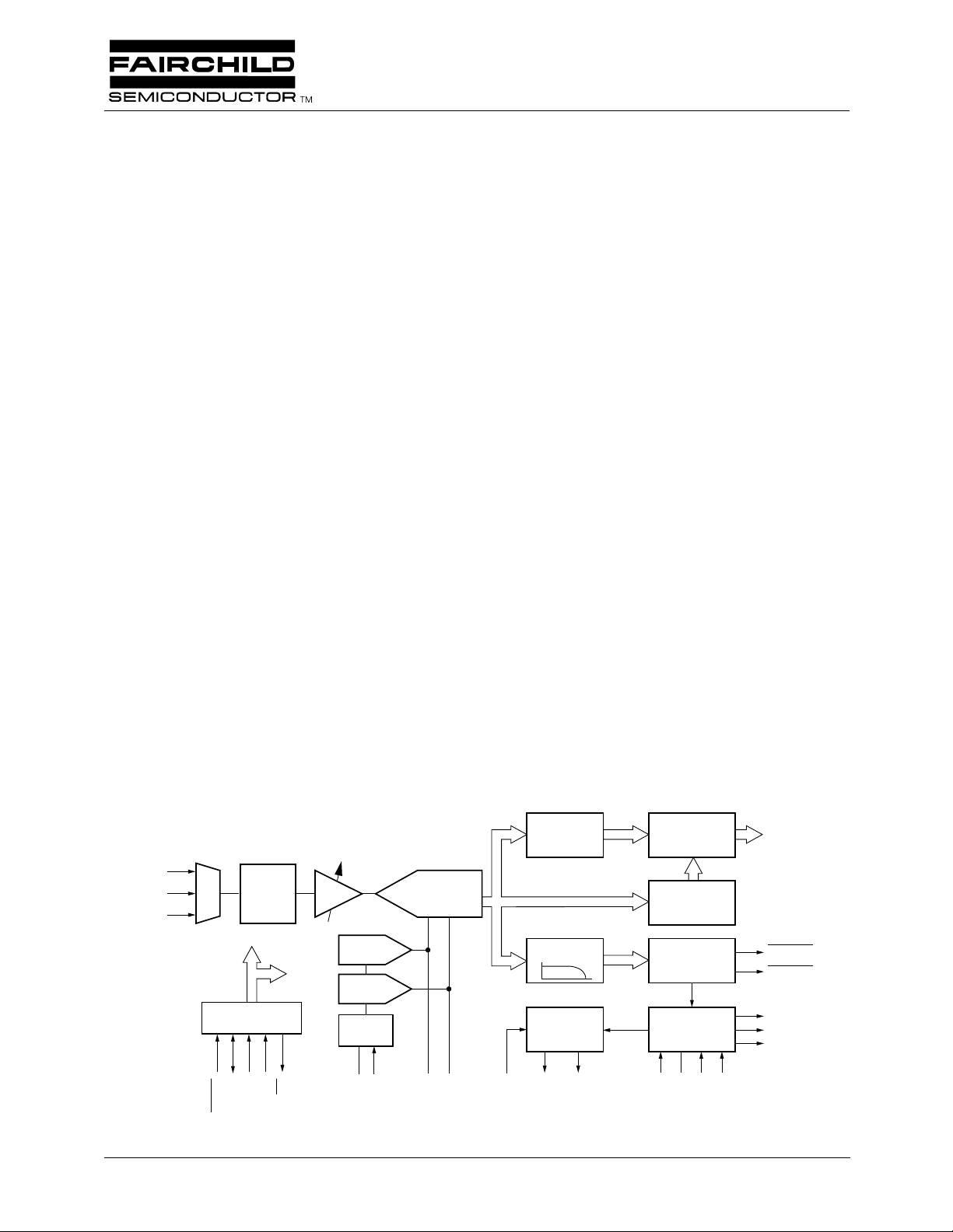
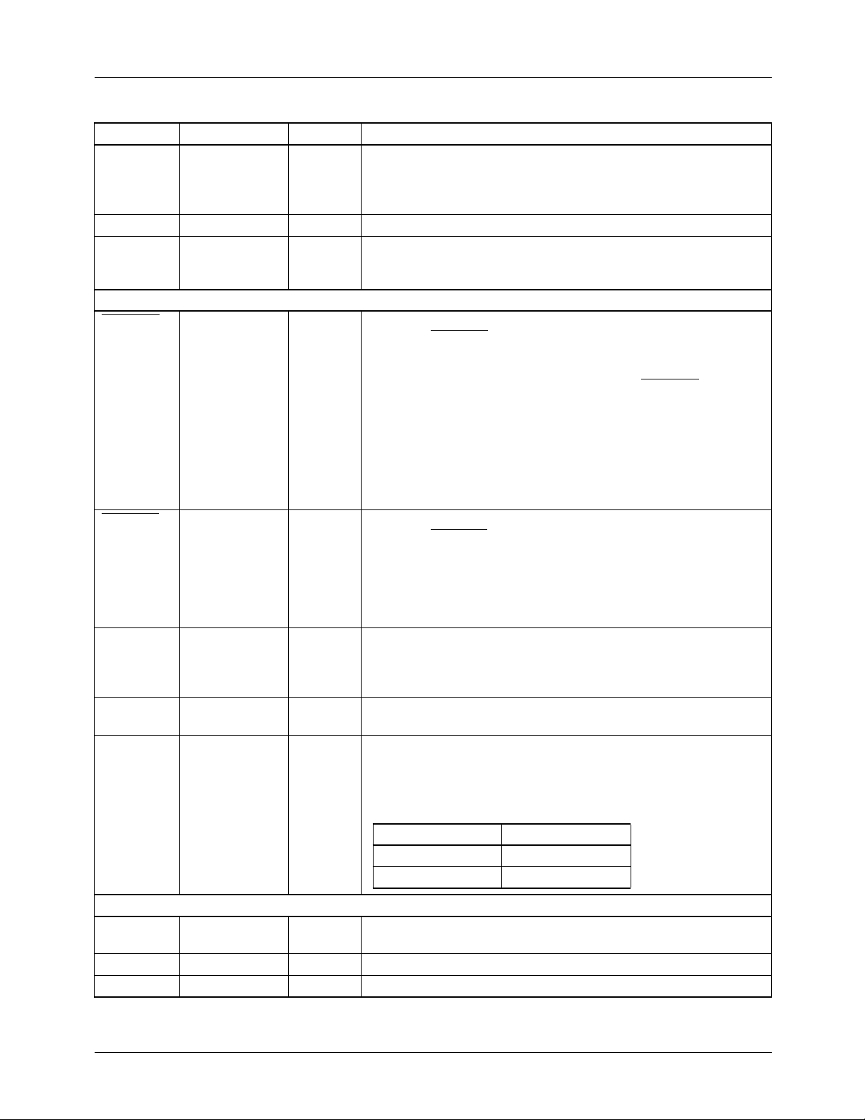
Block Diagram
V
IN1
V
IN2
V
IN3
MUX
CONTROL
RESET
MICROPROCESSOR
INTERFACE
ANALOG
CLAMP
SCL
SDA
SA
2-0
INT
BACK PORCH
CLAMP
GAIN
D/A
D/A
+1.2V
REF
V
COMP
ANALOG INTERFACE DDS/PIXEL CLOCK INTERFACE
A/D
R
LOWPASS
FILTER
DIRECT
DIGITAL
SYNTHESIZER
T
B
R
CLK IN
CLK
OUT
DDS
OUT
DATA
SELECTOR
SUBCARRIER
PHASE-LOCKED
LOOP
SYNC
SEPARATOR
HORIZONTAL
PHASE-LOCKED
LOOP
BYP
C
PFD IN
PXCK SEL
CVBS
7-0
GVSYNC
GHSYNC
PXCK
LDV
VALID
65-2072-01
EXT PXCK
REV. 1.0.4 6/19/01
Page 2

TMC2072 PRODUCT SPECIFICATION
Functional Description
The TMC2072, a fully integrated self-genlocking video A/D
converter, digitizes NTSC or PAL baseband composite signals. It accepts video on one of three input channels, adjusts
the gain, clamps to the back porch and digitizes the video at
a user-selectable multiple of the horizontal line frequency.
It extracts horizontal and vertical sync, measures the subcarrier frequency and phase, and provides these data with the
digitized composite data over an 8-bit digital video port.
Horizontal and vertical sync outputs are provided, along with
pixel clock (LDV) and twice pixel clock (PXCK).
Operating parameters are set up via a standard two-wire
microprocessor port. The chip can work with either an internal or an external voltage reference.
Fabricated in an advanced CMOS process, the TMC2072 is
housed in a 100 lead metric quad flat package. Its performance is guaranteed from 0 to 70°C and from 4.75 to 5.25
supply volts.
Timing
The TMC2072’s A/D converter and digital signal path
operate from alternate cycles of an internally-synthesized
clock, PXCK. This 24.5 to 30 MHz clock is derived from the
incoming 20 MHz reference clock and phase-locked to the
horizontal sync tips of the incoming analog video stream.
The frequency of PXCK may be set as 1560 (NTSC VGA
square pixel), 1716 (NTSC D1), 1732 (PAL D1), or 1888 or
1920 (PAL VGA) times the incoming video line rate.
Timing of the serial microprocessor interface bus is independent of the pixel clock and is described under the Microprocessor Interface section that follows Functional Description.
Video Input
Via the microprocessor interface, the user can enable one of
the chip’s three analog video input ports. Although each port
normally anticipates a standard video signal level with
286 to 300 mV between sync tip and blank, another control
register bit allows it to be used with half-power (approximately 70% amplitude) signals. Good crosstalk isolation
accommodates active video on all three inputs simultaneously. The user must provide antialias filtering and proper
line termination externally.
Analog Clamp
The front-end analog clamp ensures that the input video falls
within the active range of the A/D converter. The digitized
composite video output can be clamped to the back porch by
a secondary digital clamp.
Automatic Gain Adjustment
To accommodate approximately a ±15% range in video
signal amplitudes, the TMC2072’s on-chip AGC circuit
engages for one video frame following either: 1) initial lock
after reset; 2) loss and recovery of lock while operating; or
3) setting of control bit AGCEN high by the host microprocessor. The AGC operation adjusts the A/D converter’s onchip reference voltages until video blank causes it to output
approximately 1/4 of its full range. The chip then holds this
gain adjustment constant until a new AGC sequence is initiated by AGCEN going high or by loss and recovery of video
lock. The one-frame timeout prevents the gain control from
riding gain and trying to track noise or minor variations in
signal strength.
To handle doubly-terminated and other weak video signals,
the user should set the VGAIN control bit high, thereby
boosting video gain 50% above nominal.
Analog-to-Digital Converter
The TMC2072 contains a high-performance 8-bit A/D
converter. Its gain and offset are automatically set as a part of
the automatic gain adjustment process during initial signal
acquisition, and require no user attention.
The reference voltages to the A/D converter are set up by
internal D/A converters under automatic control during
genlock acquisition. These voltages determine the gain and
offset of the A/D converter with respect to the video level
presented at its input.
Low-Pass Filter
The digitized composite video stream is digitally low-pass
filtered to remove chrominance components from the sync
separator. Filtering provides robust operation by optimizing
the signal-to-noise ratio of the synchronizing/blanking portion of the video, improving the accuracy of the back porch
blanking level detector.
A digital sync separator provides the output sync signals,
GHSYNC and GVSYNC, and times internal operations.
Horizontal Phase-Locked Loop
A phase-locked loop generates PXCK, at twice the pixel
rate. The reference signal for the horizontal phase-locked
loop is generated by the Direct Digital Synthesizer (DDS).
The DDS output is constructed with an internal D/A converter and is output from the TMC2072 via the DDS OUT
pin. This signal is passed through an external LC filter and
input to the horizontal phase-comparator.
The frequency of the DDS output is one ninth of that of
PXCK.
A 20MHz clock is required to drive the DDS. Preferably, this
may be input to the TMC2072 via CMOS levels on the CLK
IN pin. Alternately, a 20MHz crystal may be directly
connected between CLK IN and CLK OUT with tuning
capacitors to activate the internal crystal oscillator circuitry.
2 REV. 1.0.4 6/19/01
Page 3
PRODUCT SPECIFICATION TMC2072
If incoming video is lost or disconnected after the TMC2072
has locked to it, PXCK and GRS data will continue, but
GVSYNC
and every eighth GHSYNC will cease until lock
is reestablished. The GRS will report the initial subcarrier
frequency set by the Format select bits of the Control
Register. The TMC2072 will relock to incoming video
within two frames after it is restored.
Subcarrier Phase-Locked Loop
A fully-digital phase-locked loop is used to extract the phase
and frequency of the incoming color burst. These frequency
and phase values are output over the CVBS bus during the
horizontal sync period. Fairchild’s video decoder and genlockable encoder chips will accept these data directly.
Back Porch Digital Clamp
A digital back-porch clamp is employed to ensure a constant
blanking level. It digitally offsets the data from the A/D converter to set the back porch level to precisely 3Ch for NTSC
and 40h for PAL. When the digital clamp is enabled, the
CVBS video output data is the A/D conversion result minus
the back porch level plus 3Ch (40h for PAL). The back-porch
level is low-pass filtered to minimize streaking artifacts from
subtle line-to-line variations.
Digitized Video Output
The digitized 8-bit video output is provided over an 8-bit
wide CVBS data port, synchronous with PXCK and LDV.
Subcarrier frequency, subcarrier phase, and Field ID data
(GRS) are transmitted in 4-bit nibbles over CVBS
3-0
during
the horizontal sync tip period at the PXCK rate.
Microprocessor Interface
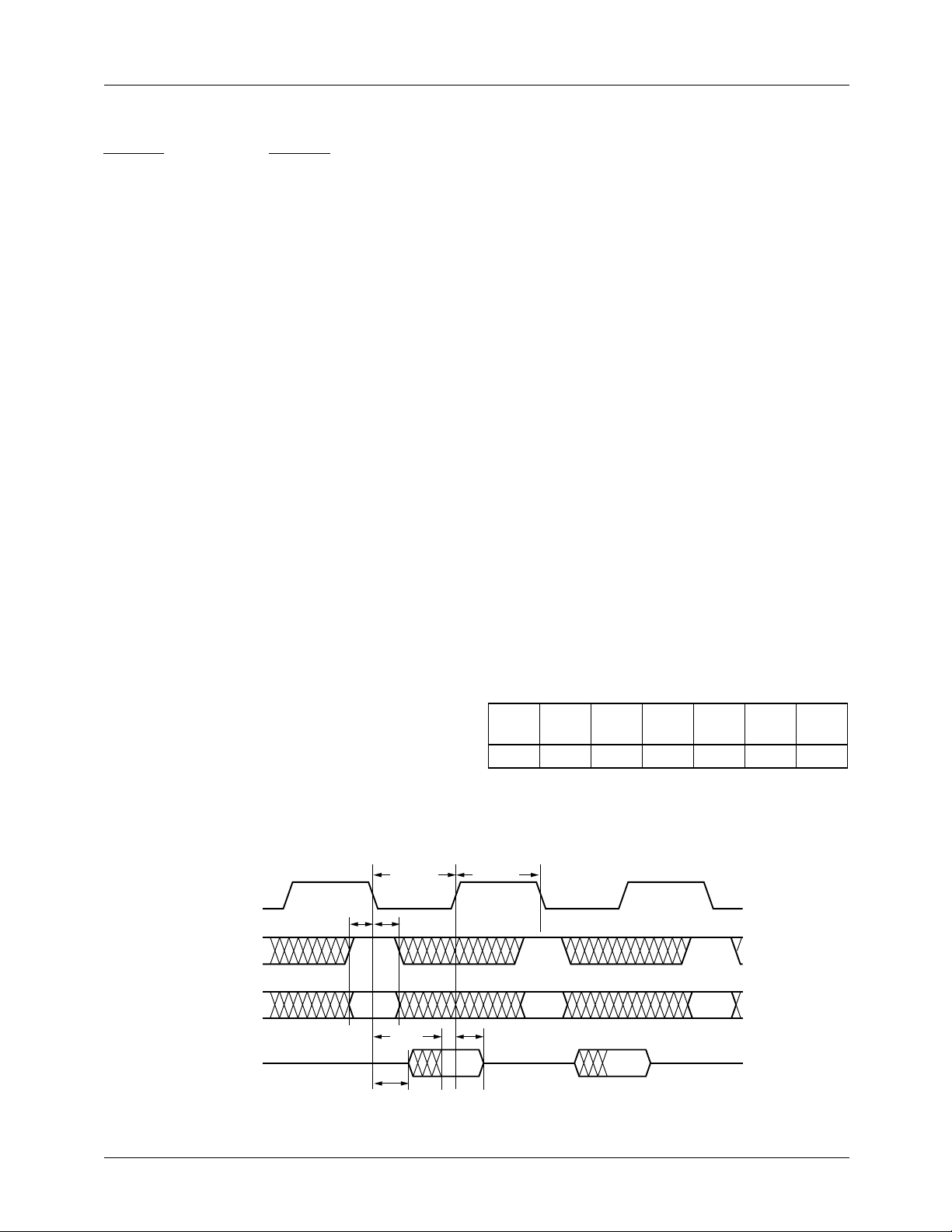
The TMC2072 is controlled by a standard 2-wire bus. Up to
eight TMC2072 devices may be connected to the 2-wire
serial interface with each device having a unique address.
The 2-wire interface comprises a clock input (SCL) and a
bi-directional data (SDA) pin. The TMC2072 acts as a slave
for receiving and transmitting data over the serial interface.
When the serial interface is not active, the logic levels on
SCL and SDA are pulled HIGH by external pull-up resistors.
Data received or transmitted on the SDA line must be stable
for the duration of the positive-going SCL pulse. Data on
SDA must change only when SCL is LOW. If SDA changes
state while SCL is HIGH, the serial interface interprets that
action as a start or stop sequence.
There are five components to serial bus operation:
• Start signal
• Slave address byte
• Base register address byte
• Data byte to read or write
• Stop signal
When the serial interface is inactive (SCL and SDA are
HIGH) communications are initiated by sending a start signal. The start signal is a HIGH-to-LOW transition on SDA
while SCL is HIGH. This signal alerts all slaved devices that
a data transfer sequence is coming.
The first eight bits of data transferred after a start signal comprise a seven bit slave address and a single R/W bit. The R/W
bit indicates the direction of data transfer, read from or write
to the slave device. If the transmitted slave address matches
the address of the device (set by the state of the SA2:0 input
pins.), the TMC2072 acknowledges by bringing SDA LOW
on the 9th SCL pulse. If the addresses do not match, the
TMC2072 does not acknowledge.
Table 1. Serial Port Addresses
A
1 0 0 0 1/0 1/0 1/0
The address is 1000 SA2 SA1 SA0.
A
6
A
5
A
4
A
3
(SA2)
A
2
(SA1)
A
1
0
(SA0)
t
PWLCS
SCL
t
SA
SDA
SA
–SA
2
0
D7–D
0
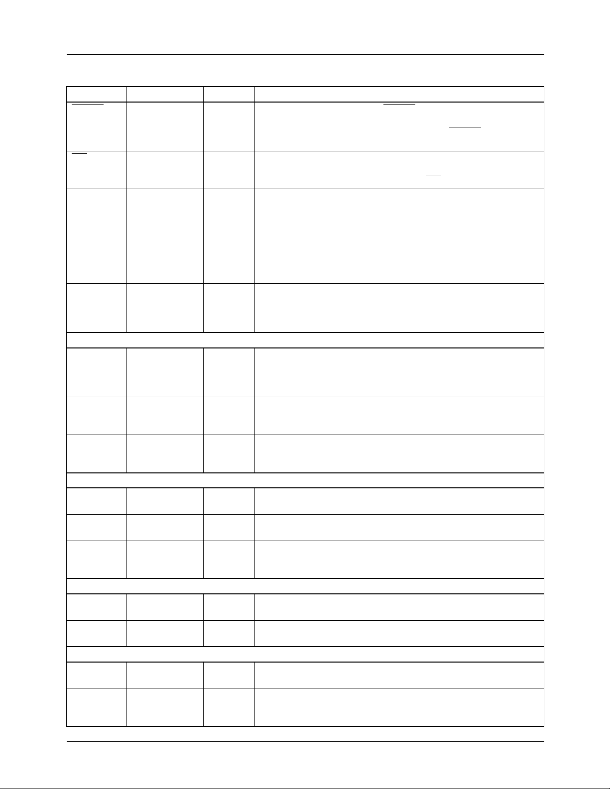
Figure 1. Microprocessor Parallel Port – Read Timing
REV. 1.0.4 6/19/01 3
t
DOZ
t
DOM
t
HA
t
PWHCS
t
DOM
65-2072-02
Page 4
TMC2072 PRODUCT SPECIFICATION
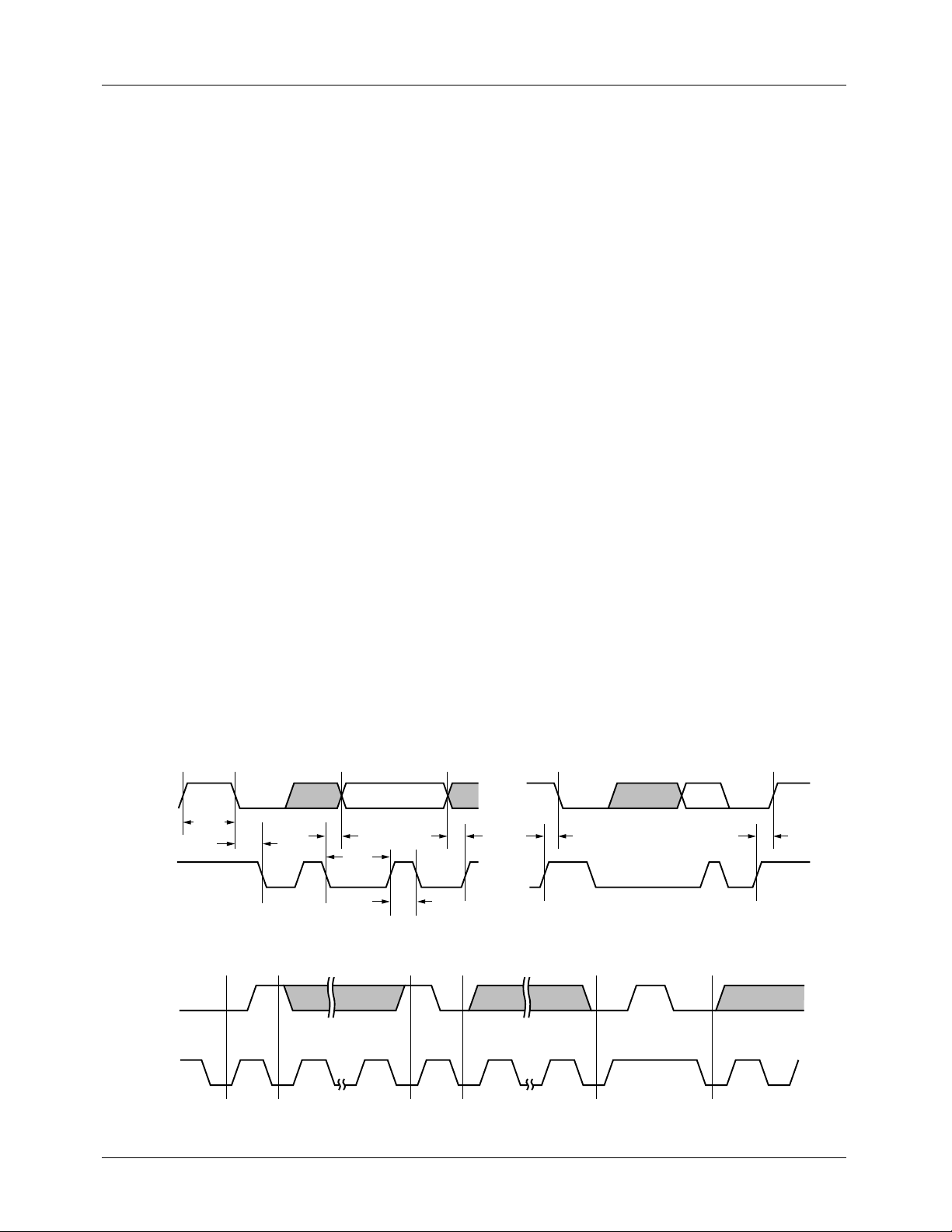
Data Transfer via Serial Interface
For each byte of data read or written, the MSB is the first bit
of the sequence.
If the TMC2072 does not acknowledge the master device
during a write sequence, the SDA remains HIGH so the master can generate a stop signal. If the master device does not
acknowledge the TMC2072 during a read sequence, the
TMC2072 interprets this as “end of data.” The SDA remains
HIGH so the master can generate a stop signal.
Writing data to specific control registers of the TMC2072
requires that the 8-bit address of the control register of interest be written after the slave address has been established.
This control register address is the base address for subsequent write operations. The base address autoincrements by
one for each byte of data written after the data byte intended
for the base address. If more bytes are transferred than there
are available addresses, the address will not increment and
remain at its maximum value of 10h. Any base address
higher than 10h will not produce an ACKnowledge signal.
If no ACKnowledge is received from the master, the encoder
will automatically stop sending data.
Data are read from the control registers of the TMC2072 in
a similar manner. Reading requires two data transfer
operations:
The base address must be written with the R/W bit of the
slave address byte LOW to set up a sequential read
operation.
Reading (the R/W bit of the slave address byte HIGH)
begins at the previously established base address. The
address of the read register autoincrements after each byte is
transferred.
To terminate a read/write sequence to the TMC2072, a stop
signal must be sent. A stop signal comprises a LOW-toHIGH transition of SDA while SCL is HIGH.
A repeated start signal occurs when the master device driving the serial interface generates a start signal without first
generating a stop signal to terminate the current communication. This is used to change the mode of communication
(read, write) between the slave and master without releasing
the serial interface lines.
Serial Interface Read/Write Examples
Write to one control register
↓ Start signal
↓ Slave Address byte (R/W bit = LOW)
↓ Base Address byte
↓ Data byte to base address
↓ Stop signal
Write to four consecutive control registers
↓ Start signal
↓ Slave Address byte (R/W bit = LOW)
↓ Base Address byte
↓ Data byte to base address
↓ Data byte to (base address + 1)
↓ Data byte to (base address + 2)
↓ Data byte to (base address + 3)
↓ Stop signal
Read from one control register
↓ Start signal
↓ Slave Address byte (R/W bit = LOW)
↓ Base Address byte
SDA
t
SCL
SDA
SCL
t
STAH
BUFF
STOP
t
DHO
t
DAL
Figure 2. Serial Port Read/Write Timing
Figure 3. Serial Interface – Start/Stop Signal
t
DSU
t
DAH
START STOP START
t
STASU
t
STOSU
65-2072-03
65-2072-04
4 REV. 1.0.4 6/19/01
Page 5
PRODUCT SPECIFICATION TMC2072
↓ Stop signal
↓ Start signal
↓ Slave Address byte (R/W bit = HIGH)
↓ Data byte from base address
↓ Stop signal
Read from four consecutive control registers
↓ Start signal
↓ Slave Address byte (R/W bit = LOW)
↓ Base Address byte
Pin Assignments
81
100
130
Note:
1. NC = No internal connection between package
and IC. Fairchild Semiconductor recommends
leaving these pins open to simplify board
upgrades to potential future genlock chips.
↓ Stop signal
↓ Start signal
↓ Slave Address byte (R/W bit = HIGH)
↓ Data byte from base address
↓ Data byte from (base address + 1)
↓ Data byte from (base address + 2)
↓ Data byte from (base address + 3)
↓ Stop signal
5180
Pin Name Pin Name
SA
1
0
SA
2
50
31
1
SA
3
2
SDA
4
SCL
5
V
6
DD
RESET
7
D
8
GND
NC
9
NC
10
NC
11
NC
12
NC
13
NC
14
NC
15
D
16
GND
INT
17
V
18
DD
NC
19
NC
20
CVBS
21
CVBS
22
CVBS
23
CVBS
24
CVBS
25
V
26
DD
D
27
GND
CVBS
28
CVBS
29
CVBS
30
BURL
31
GHSYNC
32
GVSYNC
33
VALID
34
FID0
35
FID1
36
NC
37
D
38
GND
D
39
GND
LDV
40
D
41
GND
V
42
DD
NC
43
V
44
DD
PXCK
45
D
46
0
1
2
3
4
GND
D
47
GND
V
48
DD
V
49
DDA
A
50
GND
Pin Name Pin Name
V
51
DDA
V
52
DDA
NC
53
5
6
7
NC
54
A
55
GND
NC
56
R
57
B
V
58
IN3
NC
59
V
60
DDA
V
61
IN2
NC
62
A
63
GND
V
64
DDA
V
65
IN1
NC
66
A
67
GND
R
68
T
A
69
GND
V
70
REF
NC
71
A
72
GND
V
73
DDA
A
74
GND
C
75
BYP
76
77
78
79
80
81
82
83
84
85
86
87
88
89
90
91
92
93
94
95
96
97
98
99
100
NC
PFD IN
NC
NC
NC
A
GND
DDS OUT
NC
NC
NC
PXCK SEL
V
DDA
COMP
A
GND
D
GND
CLK IN
V
DD
CLK OUT
EXT PXCK
D
GND
D
GND
D
GND
V
DD
NC
V
DD
65-2072-05
Pin Definitions
Pin Name Pin Number Pin Type Function
Video Input
V
IN1-3
Clocks
CLK IN 91 CMOS 20 MHz DDS clock input. 20 MHz CMOS clock input to DDS. This
CLK OUT 93 CMOS Inverted clock output. Inverted DDS clock output. This pin may
PXCK 45 CMOS 2x Pixel clock output. 2x oversampled line-locked clock output.
REV. 1.0.4 6/19/01 5
65, 61, 58 1.23Vp-p Composite Video Input. Video inputs,1.235 Volts peak-to-peak,
sync tip to peak color
pin may also be used along with CLK OUT for directly connecting
crystals.
also be used along with CLK IN for directly connecting a crystal.
Page 6
TMC2072 PRODUCT SPECIFICATION
Pin Definitions (continued)
Pin Name Pin Number Pin Type Function
LDV 40 CMOS Pixel clock output. Delayed pixel clock output. LDV runs at 1/2 the
rate of PXCK and its rising edge is useful for transferring CVBS
digital video from the TMC2072 to the TMC22x9x Digital Video
Encoders.
EXT PXCK 94 CMOS External PXCK input. Input for external PXCK clock source.
PXCK SEL 86 CMOS PXCK source select. Select input for internal or external PXCK.
When HIGH, the internally generated line-locked PXCK is selected.
When LOW, the external PXCK source is enabled.
Digital Video
GHSYNC
GVSYNC 33 CMOS Vertical sync output. When the TMC2072 is locked to incoming
CVBS
7-0
FID[0] 35 CMOS Odd/even (“top/bottom”) field flag. LOW denotes the first field of a
FID[1] 36 CMOS Bruch blanking flag. In PAL, LOW denotes a frame with burst
32 CMOS Horizontal sync output. When the TMC2072 is locked to incoming
video, the GHSYNC pin provides a negative-going pulse after the
falling edge of each horizontal sync pulse. When the device is
locked to a stable video signal, there is a fixed number of PXCK
clock cycles between adjacent falling edges of GHSYNC. If no video
signal is present and LEADLAG is less than 4A(hex), the TMC2072
will output normal, evenly-spaced horizontal pulses. If no video
signal is present and LEADLAG exceeds 88(hex), the TMC2072 will
omit every eighth Hsync pulse. As LEADLAG is increased from 49h
to 89h, seven out of every eight Hsyncs will be unaffected, but the
eighth will shrink by one clock cycle per LSB step, until it disappears
entirely at 89h.
video, the GVSYNC pin provides a negative-going edge after the
start of the first vertical sync pulse of a vertical blanking interval. If
no video signal is present on the selected input pin, GVSYNC will
remain continuously at logic high, until a signal is selected and lock
is reestablished. A system designer requiring a free-running vertical
sync may wish to provide this with an external pixel counter.
30-28, 25-21 CMOS Composite output bus. 8-bit composite video data are output on
this bus at 1/2 the PXCK rate. During horizontal sync, field ID,
subcarrier frequency, and subcarrier phase are available on this
bus.
video frame; HIGH, the second.
blanked on line 310, whereas HIGH denotes burst detected on line
310. FID[1] is valid only in PAL and only when FID[0] is high and
should be interpreted as follows:
FID[1:0] PAL Field Number
01 II or VI
11 IV or VIII
µP l/O
SA[2:0] 3-1 R-bus chip address, 3 LSBs. Full 7-bit address = {1, 0, 0, 0, SA[2],
SA[1], SA[0]}
SDA 4 R-bus R-bus bidirectional data line.
SCL 5 R-bus R-bus clock line (input/slave only)
6 REV. 1.0.4 6/19/01
Page 7
PRODUCT SPECIFICATION TMC2072
Pin Definitions (continued)
Pin Name Pin Number Pin Type Function
RESET
INT
VALID 34 TTL HSYNC locked flag. Hsync locked flag. When high, this output
BURL 31 TTL/
Analog Interface
V
REF
COMP 88 0.1 µF Compensation capacitor. Compensation for DDS D/A converter
RB, RT 57, 68 0.1 µF A/D V
PLL Filter
DDS OUT 82 Internal DDS output. Analog output from the internal Direct Digital
PFD IN 77 Horizontal PLL input. Analog input to the Phase/Frequency
C
BYP
Power Supply
V
DDA
V
DD
Ground
A
GND
D
GND
6, 18, 26, 42, 44,
69, 72, 74, 81, 89
8, 16, 27, 38, 39,
7 TTL Master reset input. Bringing RESET LOW forces the internal state
machines to their starting states, loads the Control Register with
default values, and disables outputs. Bringing RESET
the TMC2072 in its default mode.
17 TTL Interrupt output. This output is LOW if the internal horizontal phase
lock loop is unlocked with respect to incoming video for 128 or more
lines per field. After lock is established, INT
indicates that the most recent incoming horizontal sync has been
detected within ±16 pixels of its expected position. It goes low if no
sync is encountered during this ±16-pixel window, as during a
typical VCR headswitch line. Once the chip has locked to a clean
video source, this flag should remain high continuously. If the chip
has locked to a VCR, this flag will typically go low for one (or
sometimes two) lines at the bottom of each field.
Burst lock flag. When high, this output indicates that the chip’s
CMOS
70 +1.23 V V
75 1 µF Comparator bypass. Decoupling point for the internal comparator
49, 51, 52, 60,
64, 73, 87
48, 92, 98, 100
50, 55, 63, 67,
41, 46, 47, 90,
95-97
+5 V Analog power supply. Positive power supply to analog section.
+5 V Digital power supply. Positive power supply to digital section.
0.0 V Analog ground. Ground for analog section. All pins must be
0.0 V Digital ground. Ground for digital section. All pins must be
internal subcarrier synthesizer is phase-aligned with the current
line’s incoming chroma burst. The flag goes low when the internal
and external phases diverge.
input/output. +1.23 Volt reference. When the internal voltage
REF
reference is used, this pin should be decoupled to A
µF capacitor. An external +1.2 Volt reference may be connected
here, overriding the internal reference source.
circuitry. This pin should be decoupled to V
capacitor.
decoupling. Decoupling points for A/D converter voltage
REF
references. These pins should be decoupled to A
capacitor.
Synthesizer D/A converter, at 1/9 the PXCK frequency.
Detector of the horizontal phase-locked loop.
reference of the Phase/Frequency Detector. This pin should be
decoupled to A
All pins must be connected.
All pins must be connected.
connected.
connected.
with a 0.1 µF capacitor.
GND
goes HIGH.
DDA
HIGH restarts
GND
with a 0.1 µF
GND
with a 0.1
with a 0.1 µF
REV. 1.0.4 6/19/01 7
Page 8

TMC2072 PRODUCT SPECIFICATION
Control and Status Register Bit Functions
Summary
Register Function
Reg 00 97h (year of revision) read only
Reg 01 20h (part #) read only
Reg 02 72h (part #) read only
Reg 03 01h (silicon revision #) read only
Reg 04 Reserved
Reg 05 Lock flags; sync tip read only
Reg 06 Blank level read only
Reg 07 Reserved
Reg 08 Format; clock rate; freerun; clamp; reset
Reg 09 HSync lead/lag
Reg 0A Gain; loop filter bandwidth; subpixel sync & clk position
Reg 0B Video source select
Reg 0C Vsync delay
Reg 0D Sync tip set
Reg 0E Output timing, tristate
Reg 0F Reserved
Details
Bit Name Function
Reg 00 97h (year of revision) Read Only
Reg 01 20h (part #) Read Only
Reg 02 72h (part #) Read Only
Reg 03 01h (silicon revision #) Read Only
Reg 04 Reserved
Reg 05 Lock Flags & Sync Height Read Only
7 BURST_DET Each time a high-frequency signal is detected during a video line’s normal
expected burst interval, this flag goes high until the next line’s expected burst
period. If no high-frequency signal is present during the expected burst interval,
this flag goes low. With a standard color television signal input, this flag will be low
during vertical field groups and, in PAL, Bruch-blanked lines. [TMC22071A bit 47.]
6 BURST LOCK If the subcarrier loop is unlocked on the current video line, i.e., the subcarrier
phase error measured during burst exceeds the lock threshold, this flag goes low
until the next burst interval. If the phase error is less than the threshold, the flag is
reset high. This flag is meaningful only if HLOCK is low.
5 HLOCK During each video field, if most horizontal sync pulses arrive more than 15 pixels
before or after their expected positions, this flag will go high. If most of the field’s
incoming horizontal syncs fall within 15 pixels of their expected positions, this flag
will go low. [TMC22071A bit 56.]
4:0 ST These bits report the each line’s average sync tip level out of the A/D converter
(as observed over CVBS). For a clean signal, the reported value will match the
sync tip set in Reg 0D, below.
8 REV. 1.0.4 6/19/01
Page 9

PRODUCT SPECIFICATION TMC2072
Details (continued)
Bit Name Function
Reg 06 Blank level Read Only
7:0 BP Blank level, as measured at the low-pass-filtered A/D output during each line’s
color back porch. For a standard video input, its decimal value will be
approximately 60 (NTSC) or 64 (PAL). [TMC22071A bits 55:48.]
Reg 07 Reserved
Reg 08 Standard and Clock Rate Select
7:6 V_STD Video Standard. These two control bits select the incoming video standard, viz:
00 NTSC, NTSC-EIAJ (power-on default)
01 PALM (Brazil)
10 PALB,G,H,I
11 PALN (Argentina)
[With bits 5:4, these bits cover all functions of TMC22071A bits 3:1.]
5:4 CK_RATE Pixel Clock/Sample Rate. Pixel (sample) rate selector, as follows:
00 12.27 MHz (power-on default; 525-line VGA)
01 13.5 MHz (D1 television rate)
10 14.75 MHz (625-line square-pixel VGA) TMC2072-1 only
11 15.0 MHz TMC2072-1 only
Note: The 12.27 MHz pixel rate is reserved for 525-line television standards
(NTSC, PAL-M), whereas the 14.75 and 15.0 MHz rates are for 625-line
standards (all other PAL) only. Bit combinations 0x1x and 1x00 may yield stable
composite data samples, sync pulses, and pixel clock, but no useful color
subcarrier information.
3 FREERUN Freerun vs. Genlock Operation. LOW (power-on default): Standard genlock
mode, in which the PXCK, GHSYNC
observed sync pattern. HIGH: GHSYNC is counted down from a free-running
PXCK, which is unrelated to the incoming video. [TMC22071A bit 26.]
2 BPFOUT Genlock Reference Signal Enable. LOW (power-on default): Loop-predicted
subcarrier phase and frequency data (GRS) are sent over CVBS during each
horizontal sync pulse. HIGH: GRS data suppressed, such that the CVBS
datastream is just the digitized incoming video signal. [TMC22071A bit 33.]
1 DC_CLAMP HIGH (power-on default): vertically low-pass filtered digital porch clamp enabled.
LOW: digital clamp disabled [TMC22071A bit 34, except that the TMC22071A
clamp has no vertical filter.]
0 S_RESET Master Software Reset Control. HIGH (power-on default & self-reset state):
normal operation. LOW: Bringing this “one-shot” control low resets all internal
state machines and registers except the microprocessor control bits themselves.
The bit then sets itself high, permitting normal operation. (Because it
automatically returns to the high state, this bit will always appear as a 1 when
read through the microprocessor port.) [TMC22071A bit 0.]
Reg 09 Lead-Lag
7:0 LEAD_LAG Hsync Lead/lag Control (in one-pixel = two-PXCK increments). Power-on
default = 80 Hex. To advance (delay) GHSYNC and GVSYNC relative to the
video input, decrease (increase) the value. Program code 79h, with sub pixel
control = 0.5 will align the GHSYNC output with the falling sync edge of the input
video. [TMC22071A bits 24:17.]
, and GVSYNC lock to the incoming video’s
REV. 1.0.4 6/19/01 9
Page 10

TMC2072 PRODUCT SPECIFICATION
Details (continued)
Bit Name Function
Reg 0A Gain, loop filter, subpixel adjust
7 V_GAIN Analog Gain into A/D Converter. LOW (power-on default): unity gain, suitable
for nominal 1-volt (sync tip to reference white) video signals. HIGH: 1.5 X gain, for
over-terminated video signals with approximately 200mV sync tips. [TMC22071A
bit 9.]
6 DDS_TEST Reserved, test bit for DDSDAC; reset low (power-on default)
5 HFILT Horizontal Phase-Locked Loop Filter Bandwidth. LOW (power-on default):
narrow H loop filter to minimize jitter with clean video sources. HIGH: wide filter
bandwidth, to better accommodate jittery or noisy sources.
4:0 SUBPIX Sample Clock (and Sync Signal) Subpixel Offset Timing Control. Format is
fractional two’s complement, i.e., 0.SFFFF, where bit 4, the signed most
significant bit (S), represents 1 PXCK or 1/2 pixel. Thus, the programming range
is 01111 = +15/32 pixel to 10000 = -16/32 pixel. A value of 01000 will advance the
sample clock and syncs by 1/4 pixel relative to the incoming video, whereas a
value of 11000 will retard them the same amount. The power-on default value of
0 nominally aligns the sample clock with the center of the incoming signal’s falling
sync edges. [TMC22071A bits 16:12.]
Reg 0B Input select
7 Reserved, reset low (power-on default)
6 NCOMP Reserved, test bit: noise comparator disable; reset low (power-on default)
5:4 SOURCE These two bits determine which of the three analog input lines is active, as
follows:
00 VIN1 (power-on default)
01 VIN2
1X VIN3.
[TMC22071A bits 8:7.]
3 SCALE Reset low (power-on default) to compensate burst PLL for line-by-line changes in
sampling rate. Set high to disable compensation (test purpose only).
2:0 ANTEST Reserved, analog circuit test bits; reset low (power-on default)
Reg 0C Field and Vsync reporting
7 Reserved, reset low (power-on default)
6 FID FREE LOW (power-on default): The color frame identifier (FID[1] in NTSC) toggles
smoothly, but with no guaranteed relationship to the incoming color burst phase.
HIGH freezes FID[1] in NTSC mode, if a two-field (odd/even only) sequence is
desired.
5:3 Reserved, reset low (power-on default)
2 DLYRPTF Delay Field i.d. Update. LOW (power-on default): FID will increment at the start
of each incoming vertical sync pulse group. (NTSC lines 4 and 266.) HIGH: FID
will increment at the start of the next line after the start each incoming vertical
sync.
1 DLYRPT Delay GVSYNC Output. LOW (power-on default): TMC2072 will generate a
GVSYNC falling edge as it predicts the start of a new vertical sync series. This is
recommended for laser disk or higher quality video signals, for which the chip can
easily predict video field timing. HIGH: TMC2072 will generate a GVSYNC falling
edge on the line after it detects the start of a vertical sync series. This is
recommended for jittery input signals, if a one-line upward image displacement is
acceptable.
10 REV. 1.0.4 6/19/01
Page 11

PRODUCT SPECIFICATION TMC2072
Details (continued)
Bit Name Function
0 ENAGC Re-Enable Automatic Gain Control. HIGH (self-resetting one-shot): Initiates a
new, self-terminating one-frame AGC sequence, independent of sync lock status.
LOW (power-on default and self-reset): AGC is enabled for one frame when video
sync is initially acquired, and each time sync is lost and reacquired. [TMC22071A
bit 25].
Reg 0D Sync Tip Set
7:4 Reserved
3:0 ST[3:0] Programmable Sync Tip Value. Power-on default = 0. Recommended setting =
3. When the chip has achieved stable lock, this will be the average value output
over CVBS during sync tips and equalization pulses. [TMC22071A bit 43:40.]
Reg 0E
7 FLIPPX LOW (power-on default): Phase of PXCK output matches that of the TMC22071A.
HIGH: Phase of PXCK output is inverted, relative to that of the TMC22071A.
6 FLIPLDV LOW (power-on default): Phase of LDV output matches that of the TMC22071A.
HIGH: Phase of LDV output is inverted, relative to that of the TMC22071A.
5 XDLY LOW (power-on default): PXCK output timing matches that of TMC22071A.
HIGH: PXCK output is delayed approximately 5-10ns, to simplify interface timing
in some systems.
4 VDLY LOW (power-on default): LDV output timing matches that of TMC22071A. HIGH:
LDV output is delayed approximately 5-10ns, to simplify interface timing in some
systems.
3 ENVHCVBS LOW (power-on default): Digital outputs CVBS0-7, FID(2:0) and GV/GHSYNC
are tristated, to avoid bus contentions elsewhere on the system. HIGH: These
pins are enabled, for normal operation.
2 FORCEZERO LOW (power-on default): If the Hloop loses lock (Hlock\ goes high), the CVBS
port will output the default subcarrier frequency and cumulative phase keyed to
each GHSYNC falling edge, and the raw output of the A/D converter at all other
times. In this case, since the incoming video and internal state machine are
asynchronous, GRS data may appear anywhere along each digitized video line.
HIGH: If the Hloop loses lock, the CVBS data port will yield only the default
subcarrier phase and frequency data, and zero at all other times.
1:0 Reserved, reset low (power-on default)
Reg 0F
7:0 Reserved, reset low (power-on default)
REV. 1.0.4 6/19/01 11
Page 12

TMC2072 PRODUCT SPECIFICATION
Horizontal Timing
Horizontal line rate is determined by the V_STD control bits.
Figure 4 illustrates the horizontal blanking interval. Figure 5
completes the definition of timing parameters with vertical
blanking interval detail.
Video In
GHSYNC
t
DH
Figure 4. Horizontal Sync Timing
Burst
65-2072-06
H
0.5H
4.7 µsec
Serration
t
VD
65-2072-07
Video In
GVSYNC
GHSYNC
(Odd Field)
GHSYNC
(Even Field)
2.35 µsec PAL
2.3 µsec NTSC
Equalizing Pulse
t
DH
Figure 5. Vertical Sync timing
Programming the TMC2072
Upon power-up after bringing RESET LOW, the TMC2072
Control Register is set to default values listed previously.
These default values do not necessarily render the TMC2072
operational in any specific application. Before the TMC2072
is expected to acquire input video, its Control Register must
be loaded with control values specific to its use.
Table 2. TMC2072 Timing Options
Standard
Field
Rate (Hz)
Line
Rate (kHz)
Pixel
Rate (Mpps)
PXCK
Frequency (MHz)
NTSC, PAL-M 59.94 15.734264 12.2727+ 24.54+ 780
NTSC-D1 59.94 15.734264 13.50 27.0 858
PAL-D1 50.00 15.625 13.50 27.0 864
PAL-VGA* 50.0 15.625 14.75 29.0 944
PAL-VGA* 50.0 15.625 15.0 30.0 960
*TMC2072-1 only
Table 3. Control Register Example Data
Register Value Function
8 10h 13.5 MHz Pixel Rate
D 03h Sync tip = 3
E 08h Enable Outputs
Assumptions: Clean 1-volt (sync to ref white) signal on V
All other control registers left in power-up states.
IN1
.
Plxels
Per Line
12 REV. 1.0.4 6/19/01
Page 13

PRODUCT SPECIFICATION TMC2072
CVBS Bus Data Formats
The CVBS bus outputs a Genlock Reference Signal (GRS)
along with the 8-bit digital composite video data. The range
of output data versus video input voltage is illustrated in
Figure 6 where sync tip and blanking levels are controlled by
the digital backporch clamp of the TMC2072. During horizontal sync, the TMC2072 outputs field identification, subcarrier frequency, and subcarrier phase information on the
CVBS bus.
PAL-M
NTSC
Peak Chrominance
Peak Luminance
PAL
FEhFF
D2hCF
Field identification is output on CVBS
. The LSB,
2-0
CVBS0, will be LOW during odd fields and HIGH for even
fields. When NTSC operation is selected, CVBS
00,01,10,11 for fields 1 through 4 respectively. When PAL
operation is selected, CVBS
count 000, 001, 010, etc. to
2-0
111 for fields 1 through 8, respectively.
CVBS3 indicates V-component inversion in PAL. It is HIGH
for NTSC lines (burst 135°) and LOW for PAL lines (burst
225°)
h
Subcarrier frequency is sent out in a 24-bit binary representation in six 4-bit nibbles on CVBS
h
f
, is that of the on-chip burst PLL.
23-0
. Subcarrier frequency,
3-0
1-0
count
Back Porch
Burst
Sync Tip
Blanking
Figure 6. Output Data vs. Input Video Level
PXCK
GHSYNC
CVBS
3:0
01
2 3 57 58 59 60 61 62 63 64 65 66 67 68 69 70 71 72 73 74 75 76
PIXEL PIXEL PIXEL FID
FIELD IDENTIFICATION
Figure 7. Genlock Reference Signal (GRS) Format
Subcarrier phase, Φ
, is also sent out in a 24-bit binary
23-0
representation in six 4-bit nibbles on CVBS
the MSB.
3Ch40
03h03
f
23:20f19:16f15:12f11:8f7:4f3:0φ23:20φ19:16φ15:12φ11:8φ7:4φ3:0
h
h
65-2072-08
FREQUENCY PHASE
. Bit Φ23 is
3-0
PIXEL PIXEL
65-2072-09
PXCK
GHSYNC
LDV
CVBS
7:0
t
HO
t
DO
t
PWHPXtPWHPX
t
XL
PIXEL 0 PIXEL 1
t
XV
1/f
PXCK
65-2072-10
Figure 8. CVBS Bus Video Data Format
REV. 1.0.4 6/19/01 13
Page 14

TMC2072 PRODUCT SPECIFICATION
SDA / R/W
t
SCL/CS
t
STAH
BUFF
t
DHO
t
DAL
t
DAH
t
DSU
t
STASU
t
STOSU
24469A
Figure 9. Serial Port Read/Write Timing
SDA / R/W
SCL/CS
SDA / R/W
SCL/CS
Equivalent Circuits
MSB LSB ACK
Figure 10. Serial Interface – Typical Byte Transfer
A
6
n Substrate
A
5
A
4
A
3
A
2
Figure 10A. Chip Address with Read/Write
V
DD
SA
1
Bit
SA
0
V
DD
R/W ACK
24470A
65-3648-05
PFD IN
C
BYP
+2.4 V
2kΩ
+
–
V
DD
pp
65-2072-11
np
V
150Ω
DD
DDS OUT
65-2072-12
Figure 11. Equivalent PFD IN Circuit Figure 12. Equivalent DDS OUT Circuit
14 REV. 1.0.4 6/19/01
Page 15

PRODUCT SPECIFICATION TMC2072
V
DD
p
Output
n
65-2072-14
Input
65-2072-13
n Substrate
V
DD
p
n
Figure 13. Equivalent Digital Input Circuit Figure 14. Equivalent Digital Output Circuit
t
DOM
CS
t
HOM
D
0
0.5 V
Hi-Z
0.5 V
t
DOZ
2.0 V
0.8 V
65-2072-15
Figure 15. Transition Levels for Three-State Measurements
Absolute Maximum Ratings (beyond which the device may be damaged)
1
Parameter Min. Max. Unit
Power Supply Voltage -0.5 7.0 V
Input Voltage -0.5 VDD + 0.5 V
Digital Outputs
Applied Voltage
Forced Current
2
3,4
-0.5 VDD + 0.5 V
-6.0 6.0 mA
Short Circuit Duration (single output in HIGH state to GND) 1 sec
Temperature
Operating, Case -60 130 °C
Operating, Junction 150 °C
Lead Soldering (10 seconds) 300 °C
Vapor Phase Soldering (1 minute) 220 °C
Storage -65 150 °C
Notes:
1. Absolute maximum ratings are limiting values applied individually while all other parameters are within specified operating
conditions. Functional operation under any of these conditions is NOT implied.
2. Applied voltage must be current limited to specified range, and measured with respect to GND.
3. Forcing voltage must be limited to specified range.
4. Current is specified as conventional current, flowing into the device.
REV. 1.0.4 6/19/01 15
Page 16

TMC2072 PRODUCT SPECIFICATION
Operating Conditions (for standard temperature range)
Parameter Min. Nom. Max. Unit
V
DD
V
IH
V
IL
IOH Output Current, Logic HIGH -2.0 mA
lOL Output Current, Logic LOW 4.0 mA
V
IN
V
REF
T
A
Serial Microprocessor Interface
t
DAL
t
DAH
t
STAH
t
STASU
t
STOSU
t
BUFF
t
DSU
t
DHO
Note:
1. Timing reference points are at the 50% level.
Power Supply Voltage 4.75 5.0 5.25 V
Input Voltage, Logic HIGH
TTL Inputs 2.0 V
CMOS Inputs 2/3V
DD
DD
V
DD
Input Voltage, Logic LOW
TTL Inputs D
CMOS Inputs D
GND
GND
0.8 V
1/3 V
DD
Video Input Signal Level, Sync Tip to Peak White 0.9 1.0 1.1 V
External Reference Voltage 1.235 V
Ambient Temperature, Still Air 0 70 °C
SCL Pulse Width, LOW 1.3 µs
SCL Pulse Width, HIGH 0.6 µs
SDA Start Hold Time 0.6 µs
SCL to SDA Setup Time (START) 0.6 µs
SCL to SDA Setup Time (STOP) 0.6 ns
SDA Stop to SDA Start Hold Time 1.3 µs
SDA to SCL Data Setup Time 300 ns
SCL to SDA Hold Time 300 ns
V
V
V
Electrical Characteristics (for standard temperature range)
Parameter Conditions Min. Typ. Max. Unit
I
DD
I
REF
Power Supply Current
Reference Input Current V
IIH Input Current, Logic HIGH VDD = Max, VIN = 4.0V ±10 µA
I
IL
V
V
I
OZH
I
OZL
C
C
C
R
Note:
1. Typical I
Input Current, Logic LOW VDD = Max, VIN = 0.4V ±10 µA
Output Voltage, Logic HIGH IOH = -2.0 mA 2.4 V
OH
Output Voltage, Logic LOW IOL = 4.0 mA 0.4 V
OL
Hi-Z Output Leakage current, HIGH VDD = Max, VIN = V
Hi-Z Output Leakage current, LOW VDD = Max, VIN =GND ±10 µA
Digital Input Capacitance TA = 25°C, f = 1 Mhz 4 15 pF
l
Digital Output Capacitance TA - 25°C, f = 1 Mhz 10 pF
O
Input Capacitance, V
V
Input Resistance, V
V
with VDD = +5.0 Volts and TA = 25°C, Maximum IDD with VDD = +5.25 Volts and TA = 0°C.
DD
1
IN1-3
IN1-3
Total Current
190 230 mA
VDD = Max,
f
= 30MHz
PXCK
= +1.235V 100 µA
REF
DD
±10 µA
TA = 25°C, f = 3.58 Mhz 15 pF
50 kΩ
16 REV. 1.0.4 6/19/01
Page 17

PRODUCT SPECIFICATION TMC2072
Switching Characteristics (for standard temperature range)
Parameter Conditlons Min. Typ. Max. Unit
t
DO
t
HO
f
PCK
f
PXCK
t
PWHPX
t
PWHPX
t
DH
Output Delay Time C
= 35 pF 2 15 ns
LOAD
Output Hold Time 3 8 ns
Pixel Rate 12 15.3 MHz
Master Clock Rate TMC2072
TMC2072-1
24 27.4
30.6
MHz
PXCK Pulse Width, LOW 27 MHz 12 ns
PXCK Pulse Width, HIGH 27 MHz 12 ns
Horizontal Sync to GHSYNC For low-jitter video source,
14 pxck
Lead - Lag = 80h
t
VD
Vertical Sync to GVSYNC For low-jitter video source,
14 pxck
Lead - Lag = 80h
t
t
XL
XV
PXCK LOW to LDV HIGH FLIPPX = 0, FLIPLDV = 0 10 ns
PXCK LOW to LDV LOW XDLY = 0, VDLY = 0 6 ns
System Performance Characterlstics
Parameter Min. Typ. Max. Unit
E
E
t
AL
V
SCH
SCP
XT
Sync time-base variation
Subcarrier Phase Error
Line-lock Acquisition Time 2 frames
Channel-to-Channel Crosstalk @3.58 Mhz -35 dB
Note:
1. NTSC/PAL compliant black burst at nominal input level ±10%, frequencies nominal ±10 ppm.
1
1
±3ns
±2 degrees
Video A
Video B
Video C
Digital Supply Plane
LPF
75Ω
LPF
75Ω
LPF
75Ω
20 MHz, TTL
+5V
and must be connected
via low-impedance path
3.3 µF
3.3 µF
3.3 µF
+5V
Ferrite Bead
Analog Supply Plane*
10µF
0.1µF 0.1µF
D
V
V
V
EXT PXCK
CLK IN
CLK OUT
PXCK SEL
GND
IN1
IN2
IN3
VDDV
10µF
DDAAGND
Video Digitizer
INT
VALID
MICROPROCESSOR
TMC2072
Genlocking
INTERFACE
Figure 16. Typical Interface Circuit
RESET
SDA
DDS OUT
SCL
SA 2:0
6.8 pF
10µH
150 pF
C
BYP
0.1µF
390
0.01 µF
pF
PFD IN
COMP
V
REF
CVBS
GHSYNC
GVSYNC
PXCK
LDV
*section of supply plane beneath
analog interface circuitry
R
R
7:0
T
B
0.1µF
LM385-1.2
0.1µF
0.1µF
8
+5V
3.3KΩ
0.1µF
DIGITAL VIDEO
INTERFACE
65-2072-16
REV. 1.0.4 6/19/01 17
Page 18

TMC2072 PRODUCT SPECIFICATION
Application Notes
The TMC2072 is a complex mixed-signal VLSI circuit. It
produces CMOS digital signals at clock rates of up to 15
MHz while processing analog video inputs with a resolution
of less than a few millivolts. To maximize performance it is
important to provide an electrically quiet operating environment. The circuit shown in Figure 16 provides an optional
external 1.2V reference to the V
The internal V
source is adequate for most applications.
REF
Flltering
Inexpensive low-pass anti-aliasing filters are shown in
Figures 17 and 18. These filters would normally be inserted
in the video signal path just before the 75Ω terminating
resistor and AC-coupling capacitor for each of the three
video inputs, V
5th-order Chebyshev response with-3dB bandwidth of
6.7MHz and a group delay of 140 nanoseconds at 5MHz.
The filter of Figure 18 has been equalized for group delay in
the video signal band. Its -3dB passband is 5.5MHz while
the group delay is constant at 220 nanoseconds through the
DC to 5MHz frequency band.
Figure 17. Simple Anti-aliasing Filter
3.3 µH 3.3 µH 4.7 µH
. The filter of Figure 17 exhibits a
IN1-3
2.2µH
470 pF
input of the TMC2072.
REF
2.2µH
4.7 µH
470 pF1000 pF
65-2072-17
Table 4. Crystal Parameters
Parameter Value
Fundamental frequency 20 MHz
Tolerance ±30 ppm @ 25°C
Stability ±50 ppm, 0°C to 70°C
Load Capacitance 20 pF
Shunt Capacitance 7 pF Max.
ESR 50 Ω, Max.
TMC2072
1MΩ
300Ω
65-2072-19
20 MHz
Crystal
33 pF
CLK IN
33 pF
Figure 19. Direct Crystal Connections
CLK OUT
Grounding
The TMC2072 has separate analog and digital circuits. To
minimize digital crosstalk into the analog signals, the power
supplies and ground connections are provided over separate
pins (VDD and V
pins; D
GND
and A
In general, the best results are obtained by tying all grounds
to a solid, low-impedance ground plane. Power supply pins
should be individually decoupled at the pin. Power supply
noise isolation should be provided between analog and digital supplies via a ferrite bead inductor on the analog lead.
Ultimately all +5 Volt power to the TMC2072 should come
from the same power source.
are digital and analog power supply
DDA
are digital and analog ground pins).
GND
430 pF
750 pF 430 pF
Figure 18. Group Delay Equalizer Filter
470 pF 470 pF
2.2 µH
910 µH
65-2072-18
ground. While some systems may benefit from this strategy,
analog and digital grounds must be kept within 0.1V of each
other at all times.
Unused Video Inputs
The TMC2072's three video inputs (VIN1, VIN2, and VIN3)
are high impedance, diode-protected against moderate elec-
Another approach calls for separating analog and digital
Using a 20 MHz Crystal
In systems where a 20 MHz clock is not available, a crystal
may be used to generate the clock to the TMC2072. The
crystal must be a 20 MHz “fundamental” type, not overtone.
Specific crystal characteristics are listed in Table 4 and the
connections are shown in Figure 19.
trostatic discharge, and DC biased to approximately 1.9V.
We recommend tying any unused inputs to ground or to
VDD through a 1 MΩ resistor or a capacitor. Unused inputs
may also be left open without damaging the part. If grounded
directly, a video input port will source less than 1mA when
selected.
18 REV. 1.0.4 6/19/01
Page 19

PRODUCT SPECIFICATION TMC2072
Interface to the TMC22x5y Decoder
The TMC22x5y Digital Video Decoders have been designed
to directly interface to the TMC2072 Digital Video Genlock.
The TMC2072 is the source for TMC22x9x input signals
CVBS
in Figure 20. These signals directly connect to the
, GHSYNC, GVSYNC, LDV, and PXCK as shown
7-0
CVBS
GHSYNC
GVSYNC
GENLOCKING VIDEO DIGITIZER
TMC2072
RESET
SDA
SCL
PXCK
LDV
MICROPROCESSOR INTERFACE
Figure 20. TMC22x5y Interface Circuit
7:0
TMC22x5y. The serial microprocessor interfaces for
TMC22x5y and TMC2072 are identical. The SDA and SCL
bus signals from the host microprocessor are shared by the
TMC22x5y and TMC2072. Only SA[2:0], VALID, and INT
signals are separate from the microprocessor bus.
8
CVBS
7:0
GHSYNC
GVSYNC
PXCK
LDV
TMC22x5y
DIGITAL VIDEO DECODER
RESET
SDA
SCL
65-2072-20
Printed Circuit Board Layout
Designing with high-performance mixed-signal circuits
demands printed circuits with ground planes. Wire-wrap is
not an option. Overall system performance is strongly influenced by the board layout. Capacitive coupling from digital
to analog circuits may result in poor picture quality. Consider the following suggestions when doing the layout:
1. Keep the critical analog traces (COMP,V
DDS OUT, PFD IN, C
BYP
, and V
IN1-3
sible and as far as possible from all digital signals. The
TMC2072 should be located near the board edge, close
to the analog output connectors.
2. The digital power plane for the TMC2072 should be that
which supplies the rest of the digital circuitry. A single
power plane should be used for all of the VDD pins. If
the analog power supply for the TMC2072 is the same
as that of the system’s digital circuitry, power to the
TMC2072 V
pins should be decoupled with ferrite
DDA
beads and 0.1 µF capacitors to reduce noise.
3. The ground plane should be solid, nor cross-hatched.
Connections to the ground plane should have very short
leads.
, RT, RB,
REF
) as short as pos-
4. Decoupling capacitors should be applied liberally to
VDD pins. Remember that not all power supply pins are
created equal. They typically supply adjacent circuits on
the device, which generate varying amounts of noise.
For best results, use 0.1µF capacitors in parallel with
10µF capacitors. Lead lengths should be minimized.
Ceramic chip capacitors are the best choice.
5. If the digital power supply has a dedicated power plane
layer, it should not overlap the TMC2072, the voltage
reference or the analog outputs. Capacitive coupling of
digital power supply noise from this layer to the
TMC2072 and its related analog circuitry can degrade
performance.
6. CLK should be handled carefully. Jitter and noise on
this clock or its ground reference may degrade performance. Terminate the clock line carefully to eliminate
overshoot and ringing.
Related Products
• TMC22x9x Digital Video Encoders
• TMC2242/TMC2243/TMC2246 Video Filters
• TMC2081 Digital Video Mixer
• TMC22x5y Digital Decoders
• TMC2302 Image Manipulation Sequencer
REV. 1.0.4 6/19/01 19
Page 20

PRODUCT SPECIFICATION TMC2072
Mechanical Dimensions
100 Lead MQFP Package – 3.2mm Footprint
Symbol
A — .134 — 3.40
A1 .010 — .25 —
A2 .100 .120 2.55 3.05
B .008 3, 5
C .005 .13
D .904 .923 22.95 23.45
D1 .783 .791 19.90 20.10
E .667 .687 16.95 17.45
E1 .547 .555 13.90 14.10
e
L .028 .040 .73 1.03
N
ND
NE
α 0° 7° 0° 7°
ccc
B
e
Inches
Min. Max. Min. Max.
.015 .38
.009 .23
.0256 BSC .65 BSC
100 100
30 30
20 20
— .004 — .12
D
Pin 1 Indentifier
Millimeters
.22
D1
Notes
E1
E
Notes:
1.
All dimensions and tolerances conform to ANSI Y14.5M-1982.
2.
Controlling dimension is millimeters.
3.
Dimension "B" does not include dambar protrusion. Allowable
dambar protrusion shall be .08mm (.003in.) maximum in excess of
the "B" dimension. Dambar cannot be located on the lower radius
or the foot.
4.
5
4
"L" is the length of terminal for soldering to a substrate.
5.
"B" & "C" includes lead finish thickness.
.20 (.008) Min.
0° Min.
Datum Plane
.13 (.005) R Min.
0.076" (1.95mm) Ref
Lead Detail
L
.13 (.30)
.005 (.012)
C
R
α
See Lead Detail
AA2
A1
B
Seating Plane
Base Plane
-C-
Lead Coplanarity
ccc C
REV. 1.0.4 6/19/01 20
Page 21

TMC2072 PRODUCT SPECIFICATION
Ordering Information
Product Number Temperature Range Screening Package Package Marking
TMC2072KHC TA = 0°C to 70°C Commercial 100-Lead MQFP 2072KHC
DISCLAIMER
FAIRCHILD SEMICONDUCTOR RESERVES THE RIGHT TO MAKE CHANGES WITHOUT FURTHER NOTICE TO ANY
PRODUCTS HEREIN TO IMPROVE RELIABILITY, FUNCTION OR DESIGN. FAIRCHILD DOES NOT ASSUME ANY
LIABILITY ARISING OUT OF THE APPLICATION OR USE OF ANY PRODUCT OR CIRCUIT DESCRIBED HEREIN; NEITHER
DOES IT CONVEY ANY LICENSE UNDER ITS PATENT RIGHTS, NOR THE RIGHTS OF OTHERS.
LIFE SUPPORT POLICY
FAIRCHILD’S PRODUCTS ARE NOT AUTHORIZED FOR USE AS CRITICAL COMPONENTS IN LIFE SUPPORT DEVICES
OR SYSTEMS WITHOUT THE EXPRESS WRITTEN APPROVAL OF THE PRESIDENT OF FAIRCHILD SEMICONDUCTOR
CORPORATION. As used herein:
1. Life support devices or systems are devices or systems
which, (a) are intended for surgical implant into the body,
or (b) support or sustain life, or (c) whose failure to perform
when properly used in accordance with instructions for use
provided in the labeling, can be reasonably expected to
result in significant injury to the user.
2. A critical component is any component of a life support
device or system whose failure to perform can be
reasonably expected to cause the failure of the life support
device or system, or to affect its safety or effectiveness.
www.fairchildsemi.com
6/19/01 0.0m 003
2001 Fairchild Semiconductor Corporation
Stock#DS30002072
 Loading...