

Page 1
www.fairchildsemi.com
TMC2011A/2111A
Variable-Length Shift Register
Features
• Low power CMOS
• TMC2011A is a pin compatible replacement for the
TDC1011 and TMC2011
• TMC2211A is a pin compatible replacement for the
TMC2111
• Inputs and outputs are TTL compatible
• DC–40MHz clock rate
• Selectable delay lengths (TMC2011A: 3 to 18 stages,
TMC2111A: 1 to 16 stages)
• Special 4-bit wide mixed-delay mode (TMC2011A)
• Available in 24-pin CERDIP and plastic DIP and 28-lead
Plastic Leadless Chip Carrier
Description
The TMC2011A and TMC2111A are high-speed, byte-wide
shift registers with programmable delay lengths.
The TMC2011A can be programmed to any length between
3 and 18 stages. It offers a special split-word mode which
allows for mixed delay lengths. The TMC2011A, constructed in low-power CMOS, is pin and function compatible
with the bipolar TDC1011.
The TMC2111A is a byte-wide shift register that can be programmed to lengths of 1 to 16 stages.
Applications
• Video filtering
• High speed data registers
• Local storage registers
• Digital delay lines
• Television special effects
• Pipeline register
The TMC2011A and TMC2111A are fully synchronous,
with all operations controlled by a single master clock. Input
and output registers are positive-edge triggered D-type flipflops. The length and mode controls are also registered. Both
devices operate with a maximum clock rate of 40 MHz.
Fabricated in a submicron CMOS process, the TMC2011A
and TMC2111A are TTL-compatible, and are available in
24-pin CERDIP and Plastic DIP packages as well as a
28-lead Plastic Leadless Chip Carrier.
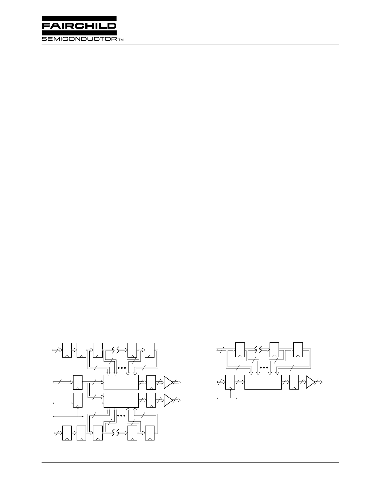
Block Diagrams
TMC2011A TMC2111A
3-0
7-4
DI
CLK
7-0
8
3-0
R
L
4
L
R
DI
3-0
L
3-0
MC
CLK
DI
R
1
R
R
R1R
2
L
I
2
4
44
7-4
4
R
3
44
1 of 16 Selector
4
1 of 16 Selector
4
R
3
R
R
16
17
44
4-Bit Wide
4-Bit Wide
R
R
18
44
R
18
444
44
4
R
16
17
DO
4
DO
65-2011A-01
R
1
88
8
8-Bit Wide
1 of 16 Selector
4
R
14
88
R
15
8
R
16
8
65-2011A-02
DO
7-0
Rev. 1.1.0
Page 2
TMC2011A/2111A PRODUCT SPECIFICATION
Functional Description
The TMC2011A consists of two 4-bit wide, programmable
length shift registers. The TMC2111A consists of a single
8-bit wide, programmable length shift register. The internal
registers of each device share control signals and a common
clock.
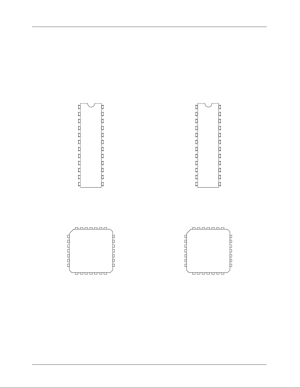
Pin Assignments
24 Lead DIP (B2, N2) Packages
DI
1
0
DI
1
DI
2
DI
3
L
0
L
1
V
DD
CLK
DI
4
DI
5
DI
6
12
DI
7
24
DO
DO
DO
DO
L
L
GND
TMC2011A
MC
DO
DO
DO
13
DO
DI
DI
DI
DI
L
L
V
DD
CLK
DI
DI
DI
DI
1
0
1
2
3
0
1
4
5
6
12
7
0
1
2
3
2
3
4
5
6
7
24
TMC2111A
13
65-2011A-03
DO
DO
DO
DO
L
2
L
3
GND
GND
DO
DO
DO
DO
0
1
2
3
4
5
6
7
28 Lead PLCC (R3) Package
DI2DI1DI0DO0DO1DO2DO
128
DI
3
L
0
L
1
V
DD
CLK
DI
NC
4
TMC2011A
7
DI5DI6DI
DO7DO6DO5DO
3
DI2DI1DI0DO0DO1DO2DO
128
NC
L
2
L
3
GND
GND
MC
NC
4
DI
V
DD
CLK
DI
NC
3
L
0
L
1
4
TMC2111A
7
DI5DI6DI
DO7DO6DO5DO
3
4
65-2011A-04
NC
L
2
L
3
GND
GND
MC
NC
2
Page 3
PRODUCT SPECIFICATION TMC2011A/2111A
Pin Descriptions – TMC2011A
Pin Number
Pin Name
Power
V
DD
GND 18 21,22 Ground. The TMC2011A operates from a single +5V supply. All power
Data Inputs
DI
7-0
Data Outputs
DO
7-0
Controls
CLK 8 9
L
3-0
MC 17 20
78 Supply Voltage. The TMC2011A and operates from a single +5V supply.
12,11,10,
9,4,3,2,1
13,14,15,
16,21,22,
23,24
19,20,6,5 23,24,7,6 Length Select. The length select input is used to determine the register
14,13,12,
10,5,4,3,2
15,16,17,
18,26,27,
28,1
Pin Function DescriptionDIP PLCC
All power and ground lines must be connected.
and ground lines must be connected.
Data Input. Eight inputs are provided for the data, which pass through the
shift register unchanged. The eight inputs on the TMC2011A are divided
into two groups of four bits to allow mixed delay operation. The lengths of
these two groups are different when the Mode Control (MC) is HIGH (see
Table 1). When MC is LOW both groups have equal delays.
Data Output. The outputs of the shift register are delayed relative to the
input signals. The amount of the delay is programmable (see Table 1).
The outputs remain valid for a minimum of t
leading edge of CLK. This allow the data to be latched into circuits with
non-zero hold time requirements.
Master Clock. All inputs and outputs are synchronous and operate from a
single master clock. All operations occur on the rising edge of the master
clock.
delay of the TMC2011A. This input is registered and affects the output t
after the clock edge after it is input to the device (see Timing Diagram).
Delay lengths are specified in Table 1.
Mode Control. The Mode Control is used to select the special 4-bit wide
split mode. When HIGH, the delay on DO
DO
have the delay specified by the length select. When MC is LOW, all
3-0
eight bits have equal delays as specified by the length select.
nanoseconds after the
HO
is fixed at 18 stages, while
7-4
DO
3
Page 4
TMC2011A/2111A PRODUCT SPECIFICATION
Pin Descriptions – TMC2111A
Pin Number
Pin Name
Power
V
DD
GND 17,18 20,21,22 Ground. The TMC2111A operates from a single +5V supply. All power
Data Inputs
DI
7-0
Data Outputs
DO
7-0
Controls
CLK 8 9
L
3-0
78 Supply Voltage. The TMC2111A operates from a single +5V supply. All
12,11,10,
9,4,3,2,1
13,14,15,
16,21,22,
23,24
19,20,6,5 23,24,7,6 Length Select. The length select input is used to determine the register
14,13,12,
10,5,4,3,2
15,16,17,
18,26,27,
28,1
Pin Function DescriptionDIP PLCC
power and ground lines must be connected.
and ground lines must be connected.
Data Input. Eight inputs are provided for the data, which pass through the
shift register unchanged. The TMC2111A consists of a single group of
eight bits with all data bits having equal delays.
Data Output. The outputs of the shift register are delayed relative to the
input signals. The amount of the delay is programmable (see Table 1).
The outputs remain valid for a minimum of t
leading edge of CLK. This allow the data to be latched into circuits with
non-zero hold time requirements.
Master Clock. All inputs and outputs are synchronous and operate from a
single master clock. All operations occur on the rising edge of the master
clock.
delay of the TMC2111A. This input is registered and affects the output t
after the clock edge after it is input to the device (see Timing Diagram).
Delay lengths are specified in Table 1.
nanoseconds after the
HO
DO
Table 1. Programming Length Controls
TMC2011A
TMC2111AInput Code Mode (MC) =0 Mode (MC) =1
L
L
3
0000333181
0001444182
0010555183
0011666184
0100777185
0101888186
0110999187
0 1 1 1 10 10 10 18 8
1 0 0 0 11 11 11 18 9
1 0 0 1 12 12 12 18 10
1 0 1 0 13 13 13 18 11
1 0 1 1 14 14 14 18 12
1 1 0 0 15 15 15 18 13
1 1 0 1 16 16 16 18 14
1 1 1 0 17 17 17 18 15
1 1 1 1 18 18 18 18 16
L
2
L
1
DO
0
Length DO
3-0
Length DO
7-4
Length DO
3-0
Length DO
7-4
7-0
Length
4
Page 5

C
PRODUCT SPECIFICATION TMC2011A/2111A
Absolute Maximum Ratings
(beyond which the device may be damaged)
Parameter Min Typ Max Unit
Supply Voltage -0.5 7.0 V
Input Voltage -0.5 V
Output, Applied Voltage
Output, Externally Forced Current
2
3,4
Output, Short Circuit Duration (single output in HIGH state to
ground)
Operating, Ambient Temperature -20 110
Junction Temperature 140
Storage Temperature -65 150
Lead Soldering (10 seconds) 300
Notes:
1. Functional operation under any of these conditions is NOT implied. Performance and reliability are guaranteed only if
Operating Conditions are not exceeded.
2. Applied voltage must be current limited to specified range.
3. Forcing voltage must be limited to specified range.
4. Current is specified as conventional current flowing into the device.
1
+ 0.5 V
DD
-0.5 V
+ 0.5 V
DD
-3.0 6.0 mA
1 sec
°
°
°
°
C
C
C
Operating Conditions
Parameter Min Nom Max Units
V
f
CLK
t
PWH
t
PWL
t
S
t
H
V
V
I
OH
I
OL
T
Power Supply Voltage 4.75 5.0 5.25 V
DD
Clock frequency TMC2011A, 2111A 30 MHz
TMC2011A-1, 2111A-1 40
CLK pulse width, HIGH 12 ns
CLK pulse width, LOW 12 ns
Input Data Set-up Time 6 ns
Input Data Hold Time 1 ns
Input Voltage, Logic HIGH DI
IH
7-0
, L
, MC 2.0 V
3-0
CLK 2.6
Input Voltage, Logic LOW 0.8 V
IL
Output Current, Logic HIGH -2.0 mA
Output Current, Logic LOW 4.0 mA
Ambient Temperature, Still Air 0 70
A
°
C
5
Page 6

TMC2011A/2111A PRODUCT SPECIFICATION
Electrical Characteristics
Parameter Conditions Min Typ Max Units
I
DDU
I
DDQ
C
I
IH
I
IL
I
OS
V
V
Power Supply Current, Unloaded V
Power Supply Current, Quiescent V
I/O Pin Capacitance 5 pF
PIN
Input Current, HIGH V
Input Current, LOW VDD = Max, VIN = 0 V ±10 mA
Short-Circuit Current -100 mA
Output Voltage, HIGH DO
OH
Output Voltage, LOW DO
OL
= Max, f
DD
V
= Max, f
DD
= Max, CLK = LOW 0.5 mA
DD
= Max, V
DD
, IOH = Max 2.4 V
7-0
, IOL = Max 0.4 V
7-0
CLK
CLK
IN
= V
=30 MHz
=40 MHz
DD
30
40
±10 mA
mA
mA
Switching Characteristics
Parameter Conditions Min Typ Max Units
t
t
DO
HO
Output Delay Time C
Output Hold Time C
= 25 pF 15 ns
LOAD
= 25 pF 3 ns
LOAD
6
Page 7

PRODUCT SPECIFICATION TMC2011A/2111A
Timing Diagrams
TMC2011A
DO
7-0
CLK 1
DI
7-0
MC, L
3-0
DO
7-0
L is Length from Table 1.
CLK
DI
7-0
L
3-0
(MC=0)
0010 0010 0011 0011 0011 0011 0011
Data
5
t
PWL
N+L+2
tSt
1/f
2
tSt
H
Data
N+L-1
H
345
Data
N+L
Data
N+L+1
t
PWH
Controls Controls Controls Controls Controls
Data
N-1
t
HO
Data
N
t
DO
Data
N+1
Data
N+2
Figure 1. Preset Length Controls
Data
10
Data
6
Data
11
Data
7
Data
12
Data
8
Data
13
Data
8
Data
14
Data
9
Data
15
Data
65-2011A-05
Data
10
Data
16
TMC2111A
DO
3-0
(MC=1)
Data
7
Equivalent Circuits
Data or
Control
Input
GND
Figure 3. Equivalent Digital Input Circuit Figure 4. Equivalent Digital Output Circuit
Data
8
Data
9
Data
10
Figure 2. Length Control Operation
V
DD
p
n
27014B
Data
10
Data
V
DD
GND
11
Data
12
65-2011A-06
p
Output
n
27011B
7
Page 8

TMC2011A/2111A PRODUCT SPECIFICATION
Notes:
8
Page 9

PRODUCT SPECIFICATION TMC2011A/2111A
Mechanical Dimensions
24-Lead Ceramic DIP Package
Symbol
A — .200 — 5.08
b1 .014 .023 .36 .58
b2 .045 1.14
c1 .008 .015 .20 .38
D — 1.280 — 32.51
E .220 .310 5.59 7.87
e
eA
L .125 .200 3.18 5.08
Q
s1
a
E
s1
Inches
Min. Max. Min. Max.
.065 1.65
.100 BSC 2.54 BSC
.300 BSC 7.62 BSC
.015 .060 .38 1.52
.005 — .13 —
90¡ 105¡ 90¡ 105¡
12
13
Millimeters
D
Notes
8
2, 8
8
4
4
5
7
3
6
Notes:
1.
Index area: a notch or a pin one identification mark shall be located
adjacent to pin one. The manufacturer's identification shall not be
used as pin one identification mark.
2.
The minimum limit for dimension "b2" may be .023 (.58mm) for leads
number 1, 12, 13 and 24 only.
3.
Dimension "Q" shall be measured from the seating plane to the base
plane.
4.
This dimension allows for off-center lid, meniscus and glass overrun.
5.
The basic pin spacing is .100 (2.54mm) between centerlines. Each
pin centerline shall be located within ±.010 (.25mm) of its exact
longitudinal position relative to pins 1 and 24.
6.
Applies to all four corners (leads number 1, 12, 13, and 24).
7.
"eA" shall be measured at the center of the lead bends or at the
centerline of the leads when "a" is 90¡.
8.
All leads – Increase maximum limit by .003 (.08mm) measured at the
center of the flat, when lead finish applied.
9.
Twenty-two spaces.
1
NOTE 1
24
e
Q
A
L
b2
b1
eA
a
c1
9
Page 10

TMC2011A/2111A PRODUCT SPECIFICATION
Mechanical Dimensions (continued)
24-Lead Plastic DIP Package
Symbol
A — .210 — 5.33
A1 .015 — .38 —
A2
B .014 .36
B1 .045 .070 1.14 1.78
C .008 .015 .20 .38 4
D 1.125 1.275 28.58 32.39
D1 .005 — .13 —
E
E1
e
eB — .430 — 10.92
L .115 .160 2.92 4.06
N
E1
Inches
Min. Max. Min. Max.
.115 .195 2.53 4.95
.022 .56
.300 .325 7.62 8.26
.240 .280 6.10 7.11
.100 BSC 2.54 BSC
24 24
12
Millimeters
D
Notes
2
2
5
1
Notes:
1.
Dimensioning and tolerancing per ANSI Y14.5M-1982.
2.
"D" and "E1" do not include mold flashing. Mold flash or protrusions
shall not exceed .010 inch (0.25mm).
3.
Terminal numbers are shown for reference only.
4.
"C" dimension does not include solder finish thickness.
5.
Symbol "N" is the maximum number of terminals.
13
D1
e
A
A1
B1
24
E
C
L
B
eB
10
Page 11

PRODUCT SPECIFICATION TMC2011A/2111A
Mechanical Dimensions (continued)
28-Lead PLCC Package
Symbol
A .165 .180 4.19 4.57
A1 .090 .120 2.29 3.05
A2 .020 .51——
B .013 .021 .33 .53
B1 .026 .032 .66 .81
D/E .485 .495 12.32 12.57
D1/E1 .450 .456 11.43 11.58
D3/E3 .300 BSC 7.62 BSC
e .050 BSC 1.27 BSC
J .042 .048 1.07 1.22 2
ND/NE 7 7
N28 28
ccc .004 0.10——
Inches
Min. Max. Min. Max.
D
D1
Millimeters
E
E1
Notes
3
J
Notes:
1.
All dimensions and tolerances conform to ANSI Y14.5M-1982
2.
Corner and edge chamfer (J) = 45¡
3.
Dimension D1 and E1 do not include mold protrusion. Allowable
protrusion is .101" (.25mm)
D3/E3
B1
e
A
A1
A2
B
J
– C –
LEAD COPLANARITY
ccc C
11
Page 12

TMC2011A/2111A PRODUCT SPECIFICATION
Ordering Information
Product
Number
Temperature
Range
Speed
Grade Screening Package
TMC2011AB2C 0°C to 70°C 30 MHz Commercial 24 Pin 0.3" CerDIP 2011AB2C
TMC2011AB2C1 0°C to 70°C 40 MHz Commercial 24 Pin 0.3" CerDIP 2011AB2C1
TMC2011AN2C 0°C to 70°C 30 MHz Commercial 24 Pin 0.3" Plastic DIP 2011AN2C
TMC2011AN2C1 0°C to 70°C 40 MHz Commercial 24 Pin 0.3" Plastic DIP 2011AN2C1
TMC2011AR3C 0°C to 70°C 30 MHz Commercial 28 Lead PLCC 2011AR3C
TMC2011AR3C1 0°C to 70°C 40 MHz Commercial 28 Lead PLCC 2011AR3C1
TMC2111AB2C 0°C to 70°C 30 MHz Commercial 24 Pin 0.3" CerDIP 2111AB2C
TMC2111AB2C1 0°C to 70°C 40 MHz Commercial 24 Pin 0.3" CerDIP 2111AB2C1
TMC2111AN2C 0°C to 70°C 30 MHz Commercial 24 Pin 0.3" Plastic DIP 2111AN2C
TMC2111AN2C1 0°C to 70°C 40 MHz Commercial 24 Pin 0.3" Plastic DIP 2111AN2C1
TMC2111AR3C 0°C to 70°C 30 MHz Commercial 28 Lead PLCC 2111AR3C
TMC2111AR3C1 0°C to 70°C 40 MHz Commercial 28 Lead PLCC 2111AR3C1
Package
Marking
LIFE SUPPORT POLICY
FAIRCHILD’S PRODUCTS ARE NOT AUTHORIZED FOR USE AS CRITICAL COMPONENTS IN LIFE SUPPORT DEVICES
OR SYSTEMS WITHOUT THE EXPRESS WRITTEN APPROVAL OF THE PRESIDENT OF FAIRCHILD SEMICONDUCTOR
CORPORATION. As used herein:
1.Life support devices or systems are devices or systems
which, (a) are intended for surgical implant into the body,
or (b) support or sustain life, and (c) whose failure to
perform when properly used in accordance with
instructions for use provided in the labeling, can be
reasonably expected to result in a significant injury of the
user.
www.fairchildsemi.com
2.A critical component in any component of a life support
device or system whose failure to perform can be
reasonably expected to cause the failure of the life support
device or system, or to affect its safety or effectiveness.
5/20/98 0.0m 001
Ó 1998 Fairchild Semiconductor Corporation
Stock#DS30002011A
 Loading...