

Page 1
www.fairchildsemi.com
Features
• 8-bit resolution
• 50 Msps conversion rate
• Low power: 100mW per channel @ 20 Msps
• Integral track/hold
• Independent Input Clamps
• Independent clock inputs
• Integral and differential linearity error 0.5 LSB
• Differential phase 0.7 degree
• Differential gain 1.8%
• Single +5V power supply
• Three-state TTL/CMOS-compatible outputs
• Low cost
Applications
• Video digitizing (composite and Y-C)
• VGA and CCD digitizing
• LCD projection panels
• Image scanners
• Personal computer video boards
• Multimedia systems
• Low cost, high speed data conversion
Description
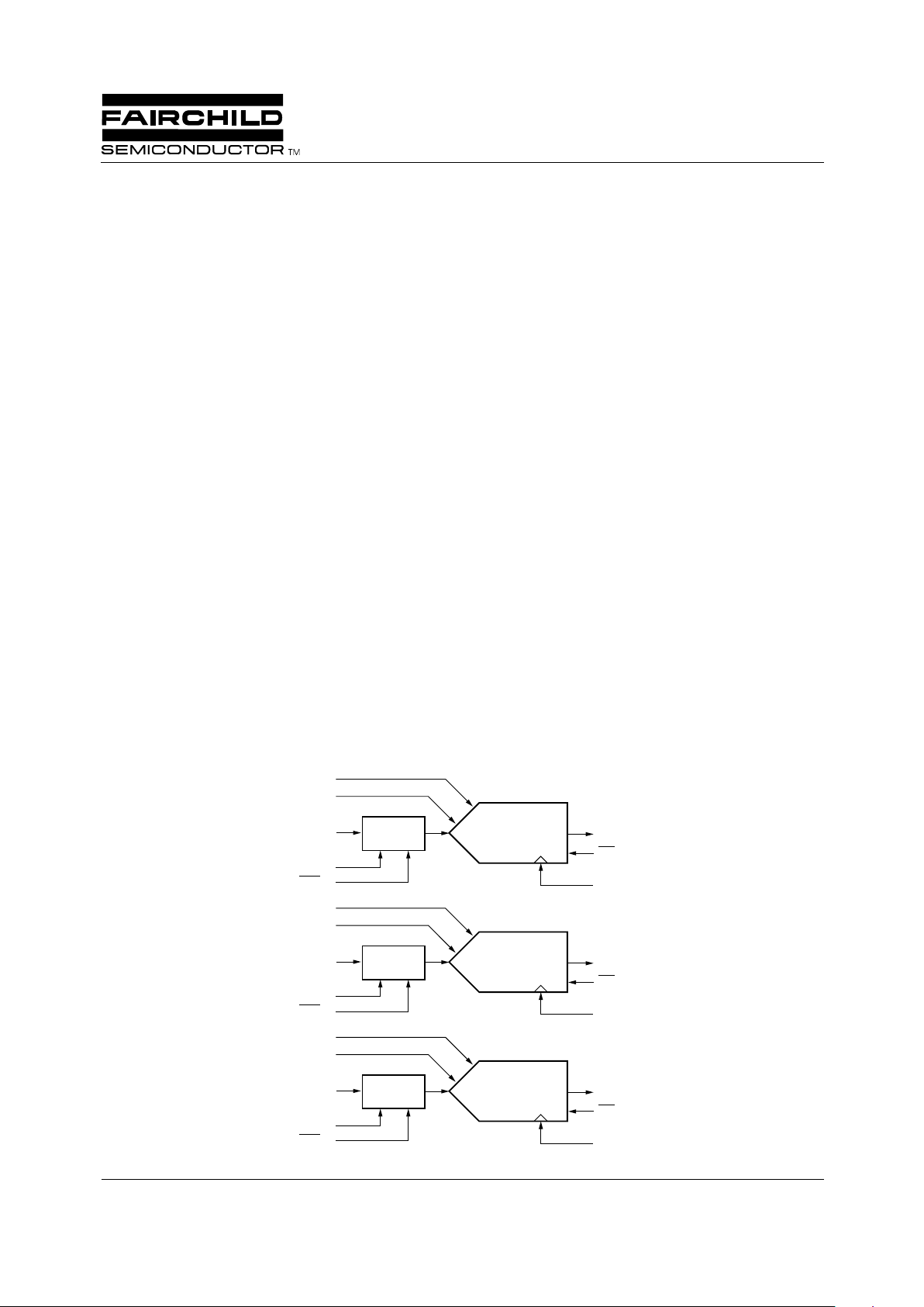
Incorporated into the TMC1103 are three analog-to-digital
(A/D) converters, each with an independent clock, reference
voltage and input clamp. Analog signals are converted to
Triple 8-bit digital words at sample rates up to 50 Msps
(Megasamples per second) per channel.
Integral Track/Hold circuits deliver excellent performance
on signals with full-scale spectral components up to
12 MHz. Innovative two-step conversion architecture and
submicron CMOS technology reduce typical power dissipation to 100 mW per converter.
Power is derived from a single +5 Volt power supply. Outputs are three-state outputs and TTL/CMOS-compatible.
TMC1103 package is a 80-lead Metric Quad Flat Pack
(MQFP). Performance specifications are guaranteed from
0°C to 70°C.
Block Diagram
8-bit
A/D Converter
R
TA
DA
7-0
OE
A
CLK
A
V
INA
V
CLPA
CLP
A
R
BA
65-1103-01
Clamp
8-bit
A/D Converter
R
TB
DA
7-0
OE
B
CLK
B
V
INB
V
CLPB
CLP
B
R
BB
Clamp
8-bit
A/D Converter
R
TC
DA
7-0
OE
C
CLK
C
V
INC
V
CLPC
CLP
C
R
BC
Clamp
TMC1103
Triple Video A/D Converter with Clamps
8-Bit, 50Msps
Rev. 1.2.0
Page 2
TMC1103 PRODUCT SPECIFICATION
2
Circuit Function
Within the TMC1103 are three 8-bit A/D converters, each
employing two-step architecture to convert an analog input
to a digital output at rates up to 50 Msps. Input signals are
held in integral track/hold stages during the conversion process. Operation is pipelined, with one input sample taken and
one output word provided for each CLKX cycle.
Each of the three converters function identically. In the following descriptions ‘X’ refers to a generic input/output or
clock where ‘X’ is equivalent to A, B or C.
The first step in the conversion process is a coarse 4-bit
quantization. This determines the range of the subsequent
fine 4-bit quantization step. To eliminate spurious codes, the
fine 4-bit A/D quantizer output is gray-coded and converted
to binary before it is combined with the coarse result to form
a complete 8-bit result.
Analog Input and Voltage References
Each A/D accepts analog signals in the range RBX to RTX into
digital data. Input signals outside this range produce “saturated” 00h or FFh output codes. The device will not
be damaged by signals within the range A
GND
to V
DDA
.
Input range is very flexible and extends from the +5 Volt
power supply to ground. Nominal input range is 2 Volts,
extending from 0.6V to 2.6V. Characterization and
performance is specified over this range. However, the
part will function with a full-scale range from 1.0V to 5.0V.
A smaller input range may simplify analog signal conditioning circuitry, at the expense of additional noise sensitivity
and some reduced differential linearity performance.
External voltage reference sources are connected to the RTX
and RBX pins. RBX can be grounded. Within each A/D converter is a reference resistor ladder comprising 255 resistors
that are accessed by the TMC1103 comparators. RTX is connected to the top of the ladder, RBX to the bottom. Gain and
offset errors are directly related to the accuracy and stability
of the applied reference voltages.
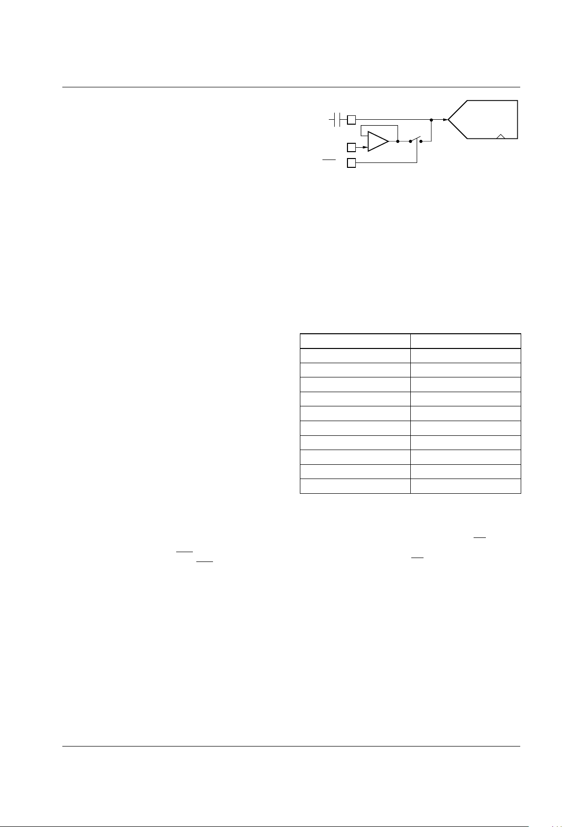
Input Clamps
A clamp circuit is connected to the input pin V
INX
of each of
the three A/D converters. With CLPX LOW, the input pin is
clamped to the voltage at V
CLPX
. If CLPX is HIGH, the
input pin is high impedance. Clamping adds an offset voltage
to an AC coupled signal to adjust this signal’s amplitude to
the A/D converter input voltage range.
The analog input is corrected through a 0.1mF capacitor to
V
INX
. The source impedance of the analog source should be
less than 50 Ohms. Current pulses through the capacitor over
several clamp cycles until the voltage across the capacitor
equals the difference between V
CLPX
and the voltage at the
analog source during the clamping period. When the switch
is open, the voltage on the coupling capacitor is added to the
analog input, producing a a DC offset input signal.
Input Clamp Circuit
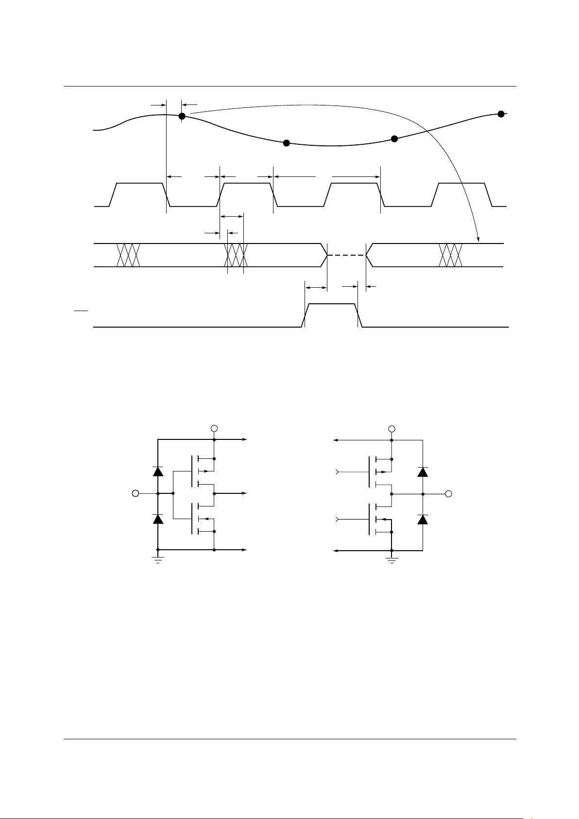
Digital Inputs and Outputs
Sampling of the applied input signal occurs on the falling
edge of the CLKX signal (Figure 1). Output data is delayed
by 2 1/2 CLKX cycles and is valid following the rising edge
of CLKX. Previous output data remains valid for tHO (Output Hold Time). New data becomes valid tD (Output Delay
Time) after this rising edge of CLKX.
Whenever the analog input signal is sampled and found to be
at a level beyond the A/D conversion range, the output limits
at 00h or FFh, as appropriate.
Table 1. A/D Output Coding
Note: 1 LSB = (RTX – RBX) / 255
The outputs of the TMC1103 are CMOS- and
TTL-compatible, and are capable of driving four low-power
Schottky TTL loads. An Output Enable control, OEX, places
the A/D outputs in a high-impedance state when HIGH.
The outputs are enabled when OEX is LOW.
Power and Ground
The TMC1103 operates from a single +5 Volt power supply.
For optimum performance, an analog ground plane should
be placed under the TMC1103 the A
GND
and D
GND
pins
should be connected to the system analog ground plane.
Input V oltage Output
RTX + 1 LSB FF
R
TX
FF
RTX - 1 LSB FE
• • • • • •
RBX + 128 LSB 80
RBX + 127 LSB 7F
• • • • • •
RBX + 1 LSB 01
R
BX
00
RBX - 1 LSB 00
A/D Converter
Analog
Input
V
INX
0.1µF
V
CLPX
CLP
X
65-1103-02
Page 3
PRODUCT SPECIFICATION TMC1103
3
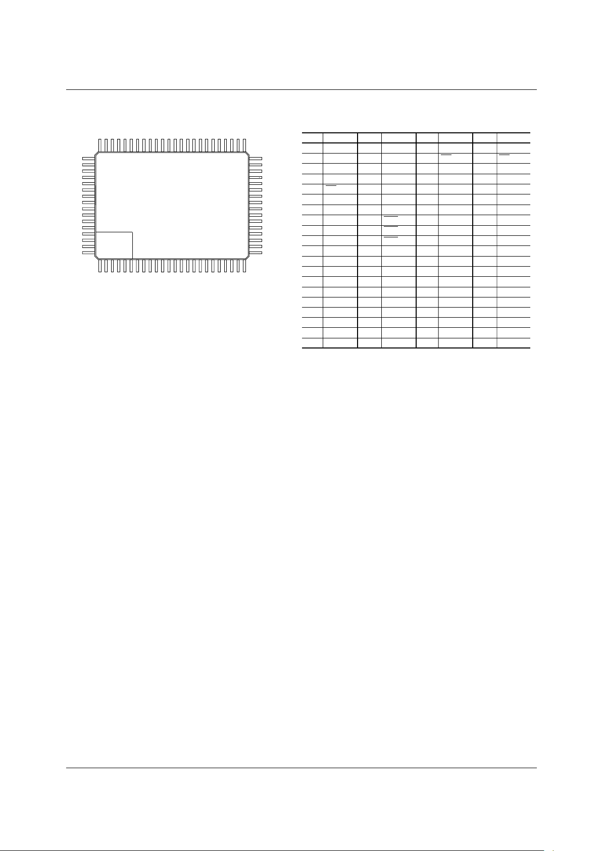
Pin Assignments
NC
DA
5
DA
6
DA
7
OE
A
V
DD
V
DD
NC
CLK
A
NC
V
DDA
V
INA
AGND
R
TA
R
BA
V
CLPA
V
CLPB
V
CLPC
DGND
DGND
1
2
3
4
5
6
7
8
9
10
11
12
13
14
15
16
17
18
19
20
DGND
DGND
NC
NC
DGND
DGND
V
DD
CLP
A
CLP
B
CLP
C
NC
DGND
DGND
DC
0
DC
1
DC
2
DC
3
DC
4
DC
5
DC
6
21
22
23
24
25
26
27
28
29
30
31
32
33
34
35
36
37
38
39
40
Pin Name Pin Name
DC
7
OE
C
V
DD
V
DD
CLK
C
NC
V
DDA
V
INC
AGND
R
TC
R
BC
R
BB
R
TB
AGND
V
INB
V
DDA
NC
CLK
B
NC
V
DD
41
42
43
44
45
46
47
48
49
50
51
52
53
54
55
56
57
58
59
60
V
DD
OE
B
DB
7
DB
6
DB
5
DB
4
DB
3
DB
2
DB
1
DB
0
DGND
DGND
NC
DGND
DGND
DA
0
DA
1
DA
2
DA
3
DA
4
61
62
63
64
65
66
67
68
69
70
71
72
73
74
75
76
77
78
79
80
Pin Name Pin Name
124
65-1103-03
25
40
4164
65
80
Page 4
PRODUCT SPECIFICATION TMC1103
4
Pin Descriptions
Pin Name Pin Number Value Pin Function Description
A/D Converters
V
INA
, V
INB
,
V
INC
12, 55, 48 RTX to
R
BX
Analog Inputs. The input voltage conversion range lies between the
voltage applied to the RTX and RBX pins.
RTA, RTB, R
TC
14, 53, 50 2.6V Reference Voltage, Top Inputs. DC voltages applied to RTA, RTB
and RTC define highest value of V
INX
.
RBA, RBB, R
BC
15, 52, 51 0.6V Reference Voltage, Bottom Inputs. DC voltages applied to RBA,
RBB and RBC define lowest value of V
INX
.
CLKA, CLKB,
CLK
C
9, 58, 45 CMOS Clock Inputs. CMOS-compatible. V
INX
is sampled on the falling
edge of CLK
X
.
DA
7-0
4, 3, 2, 80, 79,
78, 77, 76
CMOS/
TTL
Data outputs, Converter A (D7 = MSB). Eight-bit CMOS- and
TTL-compatible digital outputs. Valid data is output on the rising
edge of CLKX.
DB
7-0
63, 64, 65, 66,
67, 68, 69, 70
CMOS/
TTL
Data outputs, Converter B (D7 = MSB). Eight-bit CMOS- and
TTL-compatible digital outputs. Valid data is output on the rising
edge of CLKX.
DC
7-0
41, 40, 39, 38,
37, 36, 35, 34
CMOS/
TTL
Data outputs, Converter C (D7 = MSB). Eight-bit CMOS- and
TTL-compatible digital outputs. Valid data is output on the rising
edge of CLKX.
OEA, OEB, OE
C
5, 62, 42 CMOS Output Enable Inputs. CMOS-compatible. When LOW, the A/D
output is enabled. When HIGH, the output is in a high-impedance
state.
Clamps
V
CLPA
, V
CLPB
,
V
CLPB
16, 17, 18 RTX to
R
BX
Clamp Reference Voltage. One reference for each clamp. A V
INX
input is clamped to V
CLPX
when CLPX is low.
CLPA, CLPB,
CLP
C
28, 29, 30 CMOS Clamp Pulse Inputs. One input for each A/D clamp. When CLPX is
low, the V
INX
input is clamped to the V
CLPX
clamp voltage.
Power
V
DDA
11, 47, 56 +5V Analog Supply Voltage. +5 Volt power inputs. These should come
from the same power source and be decoupled to A
GND
.
V
DD
6, 7, 27, 28, 29,
30, 43, 44, 60,
61
+5V Digital Supply Voltage. +5 Volt power inputs. These should come
from the same power source and be decoupled to A
GND
.
A
GND
13, 49, 54 0.0V Analog Ground. Ground connections. These pins should be
connected to the system analog ground plane.
D
GND
16, 17, 18, 19,
20, 21, 22, 25,
26, 32, 33, 71,
72, 74, 75
0.0V Digital Ground. Ground connections. These pins should be
connected to the system analog ground plane.
No Connect
N/C 1, 8, 10, 23, 24,
31, 46, 57, 59,
73
open Not Connected.
Page 5
PRODUCT SPECIFICATION TMC1103
5
Figure 1. Timing
Equivalent Circuits and Threshold Levels
Figure 2. Equivalent Digital Input Circuit Figure 3. Equivalent Digital Output Circuit
V
INX
Sample N
Sample N+1
Data N-3 Data N-2 Data N-1 Data N
Hi-Z
Sample N+2
Sample N+3
t
STD
t
PWL
t
PWH
t
DIS
t
ENA
t
DO
t
HO
1/f
S
CLK
X
65-1103-04
DX
7-0
OE
X
Digital
Input
V
DD
p
n
27014B
GND
V
DD
p
n
27011B
GND
Digital
Output
Page 6

TMC1103 PRODUCT SPECIFICATION
6
Equivalent Circuits and Threshold Levels (continued)
Figure 4. Equivalent Analog Input Circuit Figure 5. Threshold Levels for Three-State Measurements
Notes:
1. Absolute maximum ratings are limiting values applied individually while all other parameters are within specified operating
conditions. Functional operation under any of these conditions is NOT implied. Performance and reliability are guaranteed
only if Operating Conditions are not exceeded.
2. Applied voltage must be current limited to specified range.
3. Forcing voltage must be limited to specified range.
4. Current is specified as conventional current flowing into the device.
Absolute Maximum Ratings (beyond which the device may be damaged)
1
Parameter Condition Min Typ Max Unit
Power Supply Voltages
VDDA Measured to A
GND
-0.5 +7.0 V
VDD Measured to D
GND
-0.5 +7.0 V
VDDA Measured to V
DD
-0.5 +0.5 V
AGND Measured to D
GND
-0.5 +0.5 V
Digital Inputs
Applied Voltage Measured to DGND -0.5 V
DD
+ 0.5 V
Forced current
-10.0 +10.0 mA
Analog Inputs
Applied Voltage Measured to A
GND
-0.5 V
DDA
+0.5 V
Forced current -10.0 +10.0 mA
Digital Outputs
Applied voltage Measured to D
GND
-0.5 VDD + 0.5 V
Forced current
-6.0 +6.0 mA
Short circuit duration Single output in HIGH state to ground) 1 second
Temperature
Operating, ambient -20 110 °C
Junction +150 °C
Lead, soldering 10 seconds +300 °C
Vapor Phase soldering 1 minute +220 °C
Storage -65 +150 °C
Electrostatic Discharge EIAJ test method ±150 V
V
DDA
V
RT
V
RB
A
GND
V
IN
29030
7048B
t
ENA
2.0V
0.8V
t
DIS
Three-State
Outputs
OE
High Impedance
0.5V
0.5V
Page 7

PRODUCT SPECIFICATION TMC1103
7
Operating Conditions
Parameter Min. Nom Max. Units
VDD, V
DDA
Power Supply Voltage 4.75 5.0 5.25 V
A
GND
Analog Ground (Measured to D
GND
) -0.1 0 0.1 V
V
RTX
Reference Voltage, Top 2.6 V
DDA
V
V
RBX
Reference Voltage, Bottom 0 0.6 V
V
RTX-VRBX
Reference Voltage Differential 1.0 2.0 5.0 V
V
INX
Analog Input Range V
RB
V
RT
V
V
CLPX
Clamp Reference Voltage, 50W max source 0 V
V
IH
Input Voltage, Logic HIGH 0.7 V
DD
V
DD
V
V
IL
Input Voltage, Logic LOW GND 0.3 V
DD
V
I
OH
Output Current, Logic HIGH -4.0 mA
I
OL
Output Current, Logic LOW 4.0 mA
T
A
Ambient Temperature, Still Air 0 70 °C
Electrical Characteristics
Parameter Conditions Min. Typ
1
Max. Units
I
DD
Power Supply Current
1
C
LOAD
= 35pF, fCK = fS (3 A/Ds)
fS = 20 Msps 70 90 mA
fS = 40 Msps 94 120 mA
fS = 50 Msps 105 135 mA
I
DDQ
Power Supply Current,
Quiescent
VDD = V
DDA
= Max.
CLKX = LOW 29 55 mA
CLKX = HIGH 45 65 mA
PD Total Power Dissipation
1
C
LOAD
= 35pF, fCK = fS (3 A/Ds)
fS = 20 Msps 300 470 mW
fS = 40 Msps 425 630 mW
fS = 50 Msps 490 710 mW
C
AI
Input Capacitance, Analog CLKX = LOW 4 pF
CLKX = HIGH 12 pF
R
IN
Input Resistance 500 kW
R
REF
Reference Resistance 200 270 340 W
I
CB
Input Current, Analog ±5 mA
I
IH
Input Current, HIGH VDD = Max., VIN = V
DD
±5 mA
I
IL
Input Current, LOW VDD = Max., VIN = 0V ±5 mA
I
OZH
Hi-Z Output Leakage Current,
Output HIGH
VDD = Max., VIN = V
DD
±5 mA
I
OZL
Hi-Z Output Leakage Current,
Output LOW
VDD = Max., VIN = V
DD
±5 mA
I
OS
Short-Circuit Current 35 mA
Page 8

TMC1103 PRODUCT SPECIFICATION
8
Note:
1. Typical values with V
DD
= V
DDA
= Nom and TA = Nom, Maximum values with VDD = V
DDA
= Max. and TA = Min.
Switching Characteristics
V
OH
Output Voltage, HIGH IOH = -2.5mA 3.5 V
IOH = Max. 2.4 V
V
OL
Output Voltage, LOW IOL = Max. 0.4 V
C
DI
Digital Input Capacitance 4 10 pF
C
DO
Digital Output Capacitance 10 pF
Parameter Conditions Min. Typ. Max. Units
f
S
Conversion Rate
TMC1103-20 20 Msps
TMC1103-40 40 Msps
TMC1103-50 50 Msps
t
PWH
CLKX Pulsewidth, HIGH
TMC1103-20 14 ns
TMC1103-40 14 ns
TMC1103-50 13 ns
t
PWL
CLKX Pulsewidth, LOW
TMC1103-20 8 ns
TMC1103-40 8 ns
TMC1103-50 7 ns
E
AP
Aperture Error 30 ps
t
STO
Sampling Time Offset 1 2 5 ns
t
STS
Sampling Time Skew 150 400 ps
t
CPW
Clamp Pulse Width
1
+20 < TA < +70°C2 mS
t
CDLY
Clamp Delay Time 100 300 ns
t
HO
Output Hold Time CLOAD = 15pF 9 ns
t
DO
Output Delay Time 14 ns
t
ENA
Output Enable Time 27 ns
t
DIS
Output Disable Time 42 ns
Electrical Characteristics (continued)
Parameter Conditions Min. Typ
1
Max. Units
Page 9

PRODUCT SPECIFICATION TMC1103
9
System Performance Characteristics
Parameter Conditions Min. Typ. Max. Units
E
LI
Integral Linearity Error,
Independent
VRT = 2.6V ±0.5 LSB
E
LD
Differential Linearity Error VRB = 0.6V ±0.5 LSB
BW Bandwidth
1
TMC1203-20 10 MHz
TMC1203-40 12 MHz
TMC1203-50 12 MHz
E
OT
Offset Voltage, Top
(RT – VIN for most positive
code transition)
VRT = 2.6V, VRB = 0.6V -40 80 mV
E
OB
Offset Voltage, Bottom
(RB – VIN for most negative
code transition)
VRT = 2.6V, VRB = 0.6V -95 -30 mV
OFF
CL
Offset Voltage, Clamp ±20 mV
dg Differential Gain fS = 14.3Msps
NTSC 40 IRE Mod Ramp
V
DDA
= +5.0V, TA=25°C
VRT = 2.6V, VRB = 0.6V
1.8 %
dp Differential Phase fS = 14.3Msps
NTSC 40 IRE Mod Ramp
V
DDA
= +5.0V, TA=25°C
VRT = 2.6V, VRB = 0.6V
0.7 deg
XTALK Channel Crosstalk fN = 5.0 MHz 45 dB
SNR Signal-to-Noise Ratio fS = 20Msps, VRT = 2.6V, VRB = 0.6V
fN = 1.24MHz 46 dB
fN = 2.48MHz 46 dB
fN = 6.98MHz 45 dB
fN = 10.0MHz 45 dB
fS = 40Msps, VRT = 2.6V, VRB = 0.6V
fN = 1.24MHz 42 dB
fN = 6.98MHz 41 dB
fN = 12.0MHz 40 dB
fS = 50Msps, VRT = 2.6V, VRB = 0.6V
fN = 1.24MHz 40 dB
fN = 6.98MHz 40 dB
fN = 12.0MHz 40 dB
Page 10

TMC1103 PRODUCT SPECIFICATION
10
Notes:
1. Bandwidth is the frequency up to which a full-scale sinewave can be digitized without spurious codes.
2. Values shown in Typ. column are typical for V
DD
= V
DDA
= +5V and TA = 25°C.
3. SNR values do not include the harmonics of the fundamental frequency.
4. SFDR is the ratio in dB of fundamental amplitude to the harmonic with the highest amplitude.
5. Characteristics specified for V
RT
= 2.6V, VRB = 0.6V.
SFDR Spurious-Free Dynamic Range fS = 20Msps, VIN = 2V p-p
fN = 1.24MHz 53 dB
fN = 2.48MHz 48 dB
fN = 6.98MHz 44 dB
fN = 10.0MHz 40 dB
fS = 40Msps, VIN = 2V p-p
fN = 1.24MHz 49 dB
fN = 6.98MHz 44 dB
f
N
= 12.0MHz 38 dB
fS = 50Msps, VIN = 2V p-p
fN = 1.24MHz 46 dB
fN = 6.98MHz 40 dB
fN = 12.0MHz 37 dB
System Performance Characteristics (continued)
Parameter Conditions Min. Typ. Max. Units
Page 11

PRODUCT SPECIFICATION TMC1103
11
Typical Performance Characteristics
Figure 6. Typical IDD vs fS (Single A/D) Figure 7. Typical SFDR vs f
IN
Figure 8. Typical SNR vs f
IN
Figure 9. Typical SNR vs Full Scale Input Range
35
30
25
20
15
10
5
0
01020
f
S
(Msps)
I
DD
30 40 50
65-1103-05
60
50
40
30
20
10
0
05
f
S
= 20Msps
10 15 20 25
fIN (Msps)
SFDR (dB)
65-1103-06
50
40
30
20
10
0
05
f
S
= 20Msps
10 15 20 25
fIN (MHz)
SNR (dB)
65-1103-07
50
40
30
20
10
0
01
f
S
= 20Msps
234 5
V
IN
SNR (dB)
65-1103-08
Page 12

TMC1103 PRODUCT SPECIFICATION
12
Figure 10. Typical Interface Circuit – High Performance
+
–
+
–
+
–
+
–
LM185-1.2
1k½
1k½
1k½
1k½
10k½
1k½
75½
100
20½
+5V
+5V
+5V
GREEN
Video
Input
GREEN
Digital
Video
Output
BLUE
Digital
Video
Output
RED
Digital
Video
Output
Pixel
Clock
0.1µF
65-1103-09
Gain Adjust
1k½
1k½
10k½
75½
100
BLUE
Video
Input
1k½
1k½
10k½
75½
100
RED
Video
Input
2k½ 0.1µF
0.1µF
0.1µF
0.1µF
0.1µF
0.1µF
VCLAMP
CLAMP
0.1µF
V
DDA
R
TA
R
TB
R
TC
R
BA
R
BB
R
BC
V
INA
V
CLPA
CLP
A
V
CLPB
CLP
B
V
CLPC
CLP
C
V
INB
V
INC
A
GNDDGND
V
DD
V
DDP
DA
7-0
OE
A
CLK
A
TMC1103
DB
7-0
OE
B
CLK
B
DC
7-0
OE
C
CLK
C
0.1µF
Application Notes
The circuit in Figure 10 employs a band-gap reference to
generate a variable RTX reference voltages for the TMC1103
as well as a bias voltage to offset the wideband input amplifiers to mid-range. The operational amplifier in the reference
circuitry is a standard 741-type.
The voltage reference at RTX can be adjusted from 0.0 to 2.4
volts while RBX is grounded. Schottky diodes can be used at
V
INX
to restrict the wideband amplifier output to between
-0.3V and VDD +0.3V. Diode protection is good practice to
limit the analog input voltage at V
INX
to the safe operating
range.
Grounding
The TMC1103 has separate analog and digital circuits. To
keep digital system noise from the A/D converter, it is recommended that power supply voltages (VDD and V
DDA
)
come from the same source, and that ground connections
(D
GND
and A
GND
) be made to the analog ground plane, and
as close as possible to the device pins. Power supply pins
should be individually decoupled at the pin. The digital circuitry that gets its input from the TMC1103 should be
referred to the system digital ground plane.
Printed Circuit Board Layout
Designing with high performance mixed-signal circuits
demands printed circuits with ground planes. Overall system
performance is strongly influenced by the board layout.
Capacitive coupling from digital to analog circuits may
result in poor A/D conversion. Consider the following suggestions when doing the layout:
1. Keep the critical analog traces (VN, RTX, RBX) as short
as possible and as far as possible from all digital signals.
The TMC1103 should be located close to the analog
input connectors.
Page 13

PRODUCT SPECIFICATION TMC1103
13
2. Segregate traces:
• A/D analog
• D/A analog
• Clocks
• Digital
Treat analog inputs as transmission lines. Cleanly route
traces over the ground plane bearing in mind that the
return currents will flow through the ground plane
beneath the traces. Do not route digital traces nearby.
A few inches of digital trace less than a few line widths
from an analog trace will cross-couple noise into
adjacent analog circuits.
3. The power plane for the TMC1103 should be separate
from that which supplies the rest of the digital circuitry.
A single power plane should be used for all of the V
DD
pins. If the power supply for the TMC1103 is the same
as that of the system's digital circuitry, power to the
TMC1103 should be decoupled with ferrite beads and
0.1mF capacitors to reduce noise.
4. The ground plane should be solid, not cross-hatched.
Connections to the ground plane should have very short
leads.
5. Decoupling capacitors should be applied liberally to
V
DD
pins. Remember that not all power supply pins
are created equal. They supply different circuits on the
integrated circuit, each of which generate varying
amounts and types of noise. For best results, use 0.1mF
ceramic capacitors. Lead lengths should be minimized.
6. CLKX should be handled carefully. Jitter and noise on
this clock may degrade performance. Terminate the
clock line, if needed, to eliminate overshoot and ringing.
Related Products
• TMC1175A, TMC1275 8-Bit Video A/D Converters
• TMC1173A, TMC1273 3V, Low-Power 8-Bit Video
A/D Converters
• TMC1203 Triple 8-bit A/D Converter
• TMC3003/TMC3503 Triple Video D/A Converters
• TMC2242B/TMC2243/TMC2246A Digital Filters
Page 14

TMC1103 PRODUCT SPECIFICATION
14
Notes:
Page 15

PRODUCT SPECIFICATION TMC1103
15
Mechanical Dimensions – 80-Lead MQFP Package
A1
-C-
LEAD COPLANARITY
Seating Plane
ccc C
See Lead Detail
Base Plane
A
A2
E
E1
D1
D
Pin 1
Identifier
B
e
Lead Detail
R
C
L
a
Datum Plane
0¡ Min.
.20 (.008) Min.
.13 (.30)
.005 (.012)
0.063" Ref (1.60mm)
A — .134 — 3.40
Symbol
Inches
Min. Max. Min. Max.
Millimeters
Notes
A1 .010 — .25 —
.018 .45
A2 .100 .120 2.55 3.05
B .012 3, 5
5
.30
.009 .23
C .005 .13
E .667 .687 16.95 17.45
.0315 BSC .80 BSC
e
L .025 .041 .65 1.03
80 80
24 24
4
N
ND
16 16
NE
a 0¡ 7¡ 0¡ 7¡
— .004 — 0.10
ccc
D .904 .923 22.95 23.45
D1 .783 .791 19.90 20.10
E1 .547 .555 13.90 14.10
Notes:
1.
2.
3.
4.
5.
All dimensions and tolerances conform to ANSI Y14.5M-1982.
Controlling dimension is millimeters.
Dimension "B" does not include dambar protrusion. Allowable
dambar protrusion shall be .08mm (.003in.) maximum in excess of
the "B" dimension. Dambar cannot be located on the lower radius
or the foot.
"L" is the length of terminal for soldering to a substrate.
"B" & "C" includes lead finish thickness.
.13 (.005) R Min.
Page 16

TMC1103 PRODUCT SPECIFICATION
6/22/98 0.0m 002
Stock# DS70001103
Ó 1998 Fairchild Semiconductor Corporation
LIFE SUPPORT POLICY
FAIRCHILD’S PRODUCTS ARE NOT AUTHORIZED FOR USE AS CRITICAL COMPONENTS IN LIFE SUPPORT DEVICES
OR SYSTEMS WITHOUT THE EXPRESS WRITTEN APPROVAL OF THE PRESIDENT OF FAIRCHILD SEMICONDUCTOR
CORPORATION. As used herein:
1. Life support devices or systems are devices or systems
which, (a) are intended for surgical implant into the body,
or (b) support or sustain life, and (c) whose failure to
perform when properly used in accordance with
instructions for use provided in the labeling, can be
reasonably expected to result in a significant injury of the
user.
2. A critical component in any component of a life support
device or system whose failure to perform can be
reasonably expected to cause the failure of the life support
device or system, or to affect its safety or effectiveness.
www.fairchildsemi.com
Ordering Information
Product Number
Conversion
Rate (Msps) Temperature Range Screening Package Package Marking
TMC1103KLC20 20 Msps TA = 0°C to 70°C Commercial 80-Lead MQFP 1103KLC20
TMC1103KLC40 40 Msps TA = 0°C to 70°C Commercial 80-Lead MQFP 1103KLC40
TMC1103KLC50 50 Msps TA = 0°C to 70°C Commercial 80-Lead MQFP 1103KLC50
 Loading...