

Page 1

®
SMALL SIGNAL SCHOTTKY DIODES
DESCRIPTION
Metal to silicon rectifier diodes in glass case featuring very low forward voltage drop and fast r ecovery
time, intended for low voltage switching mode
power supply, polarity protection and high frequency circuits.
TMBYV 10-40
MELF
(Glass)
ABSOLUTE MAXIMUM RA TINGS
(limiting values)
Symbol Parameter Val ue Unit
V
RRM
I
F (AV)
I
FSM
T
stg
T
T
L
Repetitive Peak Reverse Voltage 40 V
Average Forward Current
Surge non Repetitive Forward Current
Storage and Junction Temperature
Range
j
= 60 °C
T
i
= 25 °C
T
i
= 10ms
t
p
= 25 °C
T
i
t
= 300µs
p
Sinusoïdal Pulse
Rectangular Pulse
1A
25
50
- 65 to 150
- 65 to 125
Maximum Lead Temperature for Soldering during 15s 260
THERMAL RESISTANCE
Symbol Parameter Value Uni t
A
C
°
C
°
C
°
R
th (j - l)
* Pulse test: t
August 1999 Ed: 1A
Junction-leads 1 10
300µs δ < 2%
≤
p
C/W
°
.
1/4
Page 2
TMBYV10-40
ELECTRICAL CHARACTERISTICS
STATIC CHARACTERISTICS
Synbol T est Conditions Min. T yp. Max. Unit
I
*
R
*I
V
F
I
* * Pulse test: t
= 25°C
T
j
T
= 100°C
j
= 1A
F
= 3A 0.85
F
300µs δ < 2%
≤
p
.
V
= V
R
= 25°C
T
j
RRM
0.5
10
0.55
DYNAMIC CHARACTERISTICS
Symbol Test Conditions M in. Typ. Max. Unit
C
= 25°C VR = 0
T
j
Forward current flow in a Schottky rectifier is due
to majority carrier conduction. S o r everse recovery
is not affected by s torage charge as in conventional
PN junction diodes.
Nevertheless, when the device switches from forward biased condition to reverse blocking state,
This current depends only of diode capacitance and
external circuit impedance. Satisfactory circuit behaviour analysis may be performed assuming that
Schottky rectifier consists of an ideal diode in parallel with a variable capacitance equal to the junction capacitance (see fig. 5 page 4/4).
220 pF
current is required to charge the depletion capacitance of the diode.
mA
V
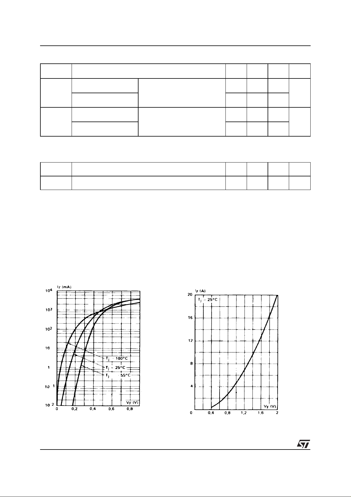
Fig. 1 :
Forward current versus forward voltage
at low level (typical values).
Fig. 2 :
Forward current versus forward voltage
at high level (typical values).
2/4
Page 3

TMBYV10-40
Fig. 3 :
Reverse current versus junction
temperature.
Fig. 4 :
cent.
Reverse current versus VRRM in per
Fig. 5 :
voltage V
Capacitance C versus reverse applied
(typical values)
R
Fig. 6 :
Surge non repetitive forward current for
a rectangular pulse with t â 10 ms.
3/4
Page 4

TMBYV10-40
Fig. 7 :
Surge non repetitive forward current
versus number of cycles.
PACKAGE MECHANICAL DATA
MELF Glass
A
REF. DIMENSIONS
Millimeters Inches
Min. T yp. Max. Min. Typ. Max.
B
/
D
O
/
C
C
FOOT PRINT DIMENSIONS (Millimeter)
3
O
A 4.80 5.20 0.189 0.205
2.50 2.65 0.098 0.104
B
∅
C 0.45 0.60 0.018 0.024
D
∅
Cooling method: by convection and conduc tion
Marking: ring at cathode end.
Weight: 0.139g
ORDERING CODE : TMB YV 10-40 F ILM
2.50 0.098
4
6.5
Information furnished is believed to be accurate and reliable. However, STMicroelectronics assumes no responsibility for
the consequences of use of such information nor for any infringement of patents or other rights of third parties which may
result from its use. No license is granted by implication or otherwise under any patent or patent rights of STMicroelectronics.
Specifications mentioned in this publicat ion are subject to change without no tice. This publication superse des and replaces
all information previously supplied.
STMicroelectronics products are not authorized for use as critical components in life support devices or systems without
express written approval of STMicroelectronics.
The ST logo is a registered trademark of STMicroelectronics
© 1999 STMicroelectronics - Printed in Italy - All rights reserved.
Australia - Brazil - China - Finland - France - Germany - Hong Kong - India - Italy - Japan - Malaysia
Malta - Morocco - Singapore - Spain - Sweden - Switzerland - United Kingdom - U.S.A.
STMicroelectronics GROUP OF COMPANIES
http://www.st.com
4/4
 Loading...