

Page 1
TK119xx
01S
VOLTAGE REGULATOR WITH RESET OUTPUT
FEATURES
■ Very Low Dropout Voltage
■ Reset Output for Microprocessor
■ Very Low Quiescent Current (No Load)
■ Internal Thermal/Overload Shutdown
■ Low Noise Voltage
■ Input and Output Voltage Sense
■ ± 2.5 % Output Voltage Accuracy
■ CMOS or TTL On/Off Control
■ High Speed On/Off Transient (50 µs typ.)
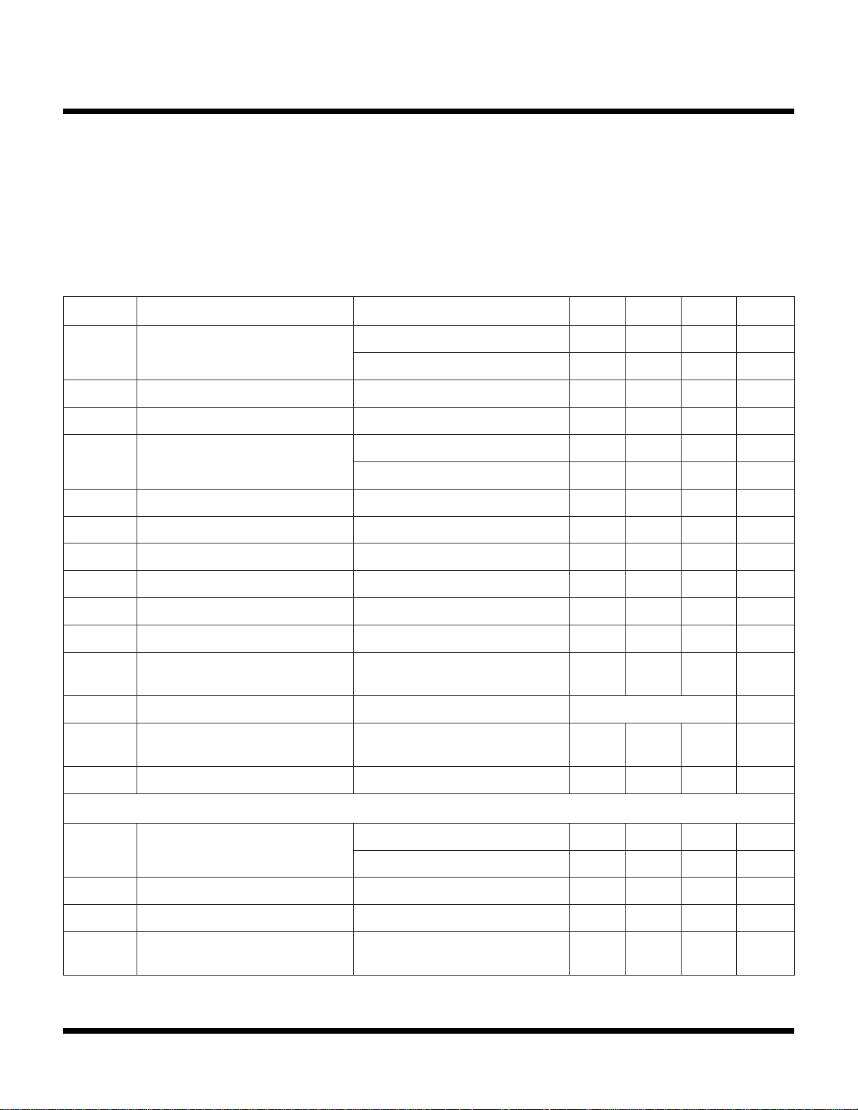
DESCRIPTION
The TK119xx series are low power, linear regulators with
built-in electronic switches. Built-in voltage comparators
provide a reset logic ”low” level whenever the input or
output voltage falls outside internally preset limits. The
internal electronic switch can be controlled by CMOS or
TLL levels. The device is in the “off” state when the control
pin is biased “high”.
An internal PNP pass-transistor is used in order to achieve
low dropout voltage (typically 200 mV at 50 mA load
current). The device has very low quiescent current
(130 µA) in the “on” mode with no load and 2 mA with 30
mA load. The quiescent current is typically 4 mA at 60 mA
load. The current consumption in the “off” mode is 65 µA.
An internal thermal shutdown circuit limits the junction
temperature to below 150 oC. The load current is internally
monitored and the device will shut down (no load current)
in the presence of a short circuit at the output. The output
noise is very low at 100 dB down from V
external noise bypass capacitor is used. The TK119xx is
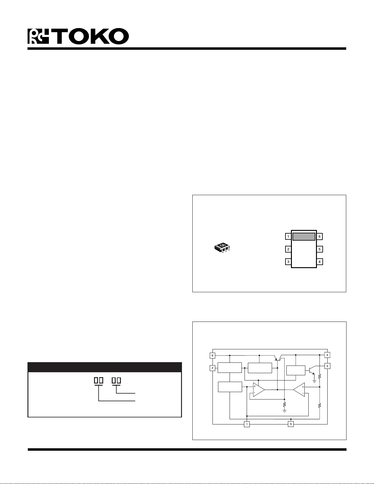
available in a miniature SOT-23L surface mount package.
ORDERING INFORMATION
when an
OUT
FEA TURES
■ Battery Powered Systems
■ Cellular Telephones
■ Pagers
■ Personal Communications Equipment
■ Portable Instrumentation
■ Portable Consumer Equipment
■ Radio Control Systems
■ Toys
■ Low Voltage Systems
TK119xx
NOISE
BYPASS
CONTROL
RESET
OUTPUT
BLOCK DIAGRAM
V
IN
CONTROL
SHUT
DOWN
THERMAL
PROTECTION
ERROR
DETECTION
V
IN
GND
V
OUT
V
OUT
RESET
OUTPUT
VOLTAGE CODE
22 = 2.25 V 35 = 2.5 V
27 = 2.75 V 40 = 4.0 V
30 = 3.00 V 48 = 4.8 V
32 = 3.25 V 50 = 5.0 V
TK119 M
Tape/Reel Code
Voltage Code
TAPE/REEL CODE
TL: Tape Left
BANDGAP
REFERENCE
NOISE
BYPASS
GND
January 1999 TOKO, Inc. Page 1
Page 2
TK119xx
ABSOLUTE MAXIMUM RATINGS
Supply Voltage ......................................................... 17 V
Operating Voltage Range............................... 1.8 to 16 V
Power Dissipation (Note 1) ................................ 400 mW
Storage Temperature Range ................... -55 to +150 °C
TK11922 ELECTRICAL CHARACTERISTICS
Test conditions: V
LOBMYSRETEMARAPSNOITIDNOCTSETNIMPYTXAMSTINU
= 3.25 V, C
IN
= 10 µF, C
L
= 0.01 µF, T
N
Operating Temperature Range ...................-30 to +80 °C
Junction Temperature .......................................... 150 °C
Lead Soldering Temperature (10 s) ..................... 235 °C
= 25 °C, unless otherwise specified.
A
I
Q
I
DNG
I
YBTS
V
TUO
V
PORD
I
TUO
tnerruCtnecseiuQ
tnerruCdnuorGI
tnerruCybdnatSFFOtuptuO59061Aµ
egatloVtuptuO
egatloVtuoporDI
tnerruCtuptuO 001Am
geReniLnoitalugeReniLV
geRdaoLnoitalugeRdaoLI
∆V
TUO
/∆T
tneiciffeoCerutarepmeT 2.0±C°/Vm
RRnoitcejeRelppiRC,zH004=f
V
ON
V
TED
V
)RRE(TED
ecnareloT
egatloVesioNtuptuO
dlohserhTrotceteDegatloV
I
TUO
V
NI
TUO
I
TUO
I
TUO
TUO
NI
TUO
C
N
Am0=041003Aµ
I,V52.1=
TUO
Am0=083009Aµ
Am06=5.201Am
T,Am1=
A
C°52=71.252.233.2V
03-,Am1= ≤ TA≤ C°0831.252.273.2V
Am03=061053Vm
V52.21ot52.3=505Vm
Am08ot1=02001Vm
L
zH01 ≤ f ≤ C,zHk001
Fµ01=86Bd
L
,Fµ01=
Fµ10.0=
dlohserhTrotceteDegatloVwoL V
4-V
05smrVµ
59.0xV
TUO
TED
4+%
V
TESER
egatloVnoitarutaSI
GALF
Aµ001=2.04.0V
SNOITACIFICEPSLANIMRETLORTNOC
I
TNOC
V
V
T
Note 1: Power dissipation is 400 mW when mounted as recommended. Derate at 3.2 mW/°C for operation above 25°C.
)NO(TNOC
)FFO(TNOC
R
emiTesiRtuptuO
tnerruClanimreTlortnoC
V
)NO(egatloVlortnoCNOtuptuO6.0V
)FFO(egatloVlortnoCFFOtuptuO2.2V
I
)NOotFFO(
TUO
C
N
V
V5=52001Aµ
TNOC
V61=54051Aµ
TNOC
C,Am03=
L
Fµ1.0=
,Fµ1.0=
05sµ
Page 2 January 1999 TOKO, Inc.
Page 3

TK11927 ELECTRICAL CHARACTERISTICS
Test conditions: V
LOBMYSRETEMARAPSNOITIDNOCTSETNIMPYTXAMSTINU
= 3.75 V, C
IN
= 10 µF, C
L
= 0.01 µF, T
N
= 25 °C, unless otherwise specified.
A
TK119xx
I
Q
I
DNG
I
YBTS
V
TUO
V
PORD
I
TUO
tnerruCtnecseiuQ
tnerruCdnuorGI
tnerruCybdnatSFFOtuptuO59061Aµ
egatloVtuptuO
egatloVtuoporDI
tnerruCtuptuO 001Am
geReniLnoitalugeReniLV
geRdaoLnoitalugeRdaoLI
∆V
TUO
/∆T
tneiciffeoCerutarepmeT 2.0±C°/Vm
RRnoitcejeRelppiRC,zH004=f
V
ON
V
TED
V
)RRE(TED
ecnareloT
egatloVesioNtuptuO
dlohserhTrotceteDegatloV
I
TUO
V
NI
TUO
I
TUO
I
TUO
TUO
NI
TUO
C
N
Am0=041003Aµ
I,V57.1=
TUO
Am0=083009Aµ
Am06=5.201Am
T,Am1=
A
C°52=76.257.238.2V
03-,Am1= ≤ TA≤ C°0836.257.278.2V
Am03=061053Vm
V57.21ot57.3=505Vm
Am08ot1=02001Vm
L
zH01 ≤ f ≤ C,zHk001
Fµ01=86Bd
L
,Fµ01=
Fµ10.0=
dlohserhTrotceteDegatloVwoL V
4-V
05smrVµ
59.0xV
TUO
TED
4+%
V
TESER
egatloVnoitarutaSI
GALF
Aµ001=2.04.0V
SNOITACIFICEPSLANIMRETLORTNOC
I
TNOC
V
V
T
)NO(TNOC
)FFO(TNOC
R
emiTesiRtuptuO
tnerruClanimreTlortnoC
V
)NO(egatloVlortnoCNOtuptuO6.0V
)FFO(egatloVlortnoCFFOtuptuO4.2V
I
)NOotFFO(
TUO
C
N
V
V5=52001Aµ
TNOC
V61=54051Aµ
TNOC
C,Am03=
L
Fµ1.0=
,Fµ1.0=
05sµ
January 1999 TOKO, Inc. Page 3
Page 4
TK119xx
TK11930 ELECTRICAL CHARACTERISTICS
Test conditions: V
LOBMYSRETEMARAPSNOITIDNOCTSETNIMPYTXAMSTINU
= 4.0 V, C
IN
= 10 µF, C
L
= 0.01 µF, T
N
= 25 °C, unless otherwise specified.
A
I
Q
I
DNG
I
YBTS
V
TUO
V
PORD
I
TUO
tnerruCtnecseiuQ
tnerruCdnuorGI
tnerruCybdnatSFFOtuptuO59061Aµ
egatloVtuptuO
egatloVtuoporDI
tnerruCtuptuO 001Am
geReniLnoitalugeReniLV
geRdaoLnoitalugeRdaoLI
∆V
TUO
/∆T
tneiciffeoCerutarepmeT 2.0±C°/Vm
RRnoitcejeRelppiRC,zH004=f
V
ON
V
TED
V
)RRE(TED
ecnareloT
egatloVesioNtuptuO
dlohserhTrotceteDegatloV
I
TUO
V
NI
TUO
I
TUO
I
TUO
TUO
NI
TUO
C
N
Am0=041003Aµ
I,V0.2=
TUO
Am0=083009Aµ
Am06=5.201Am
T,Am1=
A
C°52=29.20.380.3V
03-,Am1= ≤ TA≤ C°0888.20.321.3V
Am03=061053Vm
V0.31ot0.4=505Vm
Am08ot1=02001Vm
L
zH01 ≤ f ≤ C,zHk001
Fµ01=86Bd
L
,Fµ01=
Fµ10.0=
dlohserhTrotceteDegatloVwoL V
4-V
05smrVµ
59.0xV
TUO
TED
4+%
V
TESER
egatloVnoitarutaSI
GALF
Aµ001=2.04.0V
SNOITACIFICEPSLANIMRETLORTNOC
I
TNOC
V
V
T
)NO(TNOC
)FFO(TNOC
R
emiTesiRtuptuO
tnerruClanimreTlortnoC
V
)NO(egatloVlortnoCNOtuptuO6.0V
)FFO(egatloVlortnoCFFOtuptuO4.2V
I
)NOotFFO(
TUO
C
N
V
V5=52001Aµ
TNOC
V61=54051Aµ
TNOC
C,Am03=
L
Fµ1.0=
,Fµ1.0=
05sµ
Page 4 January 1999 TOKO, Inc.
Page 5

TK11932 ELECTRICAL CHARACTERISTICS
Test conditions: V
LOBMYSRETEMARAPSNOITIDNOCTSETNIMPYTXAMSTINU
= 4.25 V, C
IN
= 10 µF, C
L
= 0.01 µF, T
N
= 25 °C, unless otherwise specified.
A
TK119xx
I
Q
I
DNG
I
YBTS
V
TUO
V
PORD
I
TUO
tnerruCtnecseiuQ
tnerruCdnuorGI
tnerruCybdnatSFFOtuptuO59061Aµ
egatloVtuptuO
egatloVtuoporDI
tnerruCtuptuO 001Am
geReniLnoitalugeReniLV
geRdaoLnoitalugeRdaoLI
∆V
TUO
/∆T
tneiciffeoCerutarepmeT 2.0±C°/Vm
RRnoitcejeRelppiRC,zH004=f
V
ON
V
TED
V
)RRE(TED
ecnareloT
egatloVesioNtuptuO
dlohserhTrotceteDegatloV
I
TUO
V
NI
TUO
I
TUO
I
TUO
TUO
NI
TUO
C
N
Am0=041003Aµ
I,V52.2=
TUO
Am0=083009Aµ
Am06=5.201Am
T,Am1=
A
C°52=71.352.333.3V
03-,Am1= ≤ TA≤ C°0831.352.373.3V
Am03=061053Vm
V52.31ot52.4=505Vm
Am08ot1=02001Vm
L
zH01 ≤ f ≤ C,zHk001
Fµ01=86Bd
L
,Fµ01=
Fµ10.0=
dlohserhTrotceteDegatloVwoL V
4-V
05smrVµ
59.0xV
TUO
TED
4+%
V
TESER
egatloVnoitarutaSI
GALF
Aµ001=2.04.0V
SNOITACIFICEPSLANIMRETLORTNOC
I
TNOC
V
V
T
)NO(TNOC
)FFO(TNOC
R
emiTesiRtuptuO
tnerruClanimreTlortnoC
V
)NO(egatloVlortnoCNOtuptuO6.0V
)FFO(egatloVlortnoCFFOtuptuO4.2V
I
)NOotFFO(
TUO
C
N
V
V5=52001Aµ
TNOC
V61=54051Aµ
TNOC
C,Am03=
L
Fµ1.0=
,Fµ1.0=
05sµ
January 1999 TOKO, Inc. Page 5
Page 6

TK119xx
TK11935 ELECTRICAL CHARACTERISTICS
Test conditions: V
LOBMYSRETEMARAPSNOITIDNOCTSETNIMPYTXAMSTINU
= 4.5 V, C
IN
= 10 µF, C
L
= 0.01 µF, T
N
= 25 °C, unless otherwise specified.
A
I
Q
I
DNG
I
YBTS
V
TUO
V
PORD
I
TUO
tnerruCtnecseiuQ
tnerruCdnuorGI
tnerruCybdnatSFFOtuptuO59061Aµ
egatloVtuptuO
egatloVtuoporDI
tnerruCtuptuO 001Am
geReniLnoitalugeReniLV
geRdaoLnoitalugeRdaoLI
∆V
TUO
/∆T
tneiciffeoCerutarepmeT 2.0±C°/Vm
RRnoitcejeRelppiRC,zH004=f
V
ON
V
TED
V
)RRE(TED
ecnareloT
egatloVesioNtuptuO
dlohserhTrotceteDegatloV
I
TUO
V
NI
TUO
I
TUO
I
TUO
TUO
NI
TUO
C
N
Am0=041003Aµ
I,V5.2=
TUO
Am0=083009Aµ
Am06=5.201Am
T,Am1=
A
C°52=14.305.395.3V
03-,Am1= ≤ TA≤ C°0873.305.336.3V
Am03=061053Vm
V5.31ot5.4=505Vm
Am08ot1=02001Vm
L
zH01 ≤ f ≤ C,zHk001
Fµ01=86Bd
L
,Fµ01=
Fµ10.0=
dlohserhTrotceteDegatloVwoL V
4-V
05smrVµ
59.0xV
TUO
TED
4+%
V
TESER
egatloVnoitarutaSI
GALF
Aµ001=2.04.0V
SNOITACIFICEPSLANIMRETLORTNOC
I
TNOC
V
V
T
)NO(TNOC
)FFO(TNOC
R
emiTesiRtuptuO
tnerruClanimreTlortnoC
V
)NO(egatloVlortnoCNOtuptuO6.0V
)FFO(egatloVlortnoCFFOtuptuO4.2V
I
)NOotFFO(
TUO
C
N
V
V5=52001Aµ
TNOC
V61=54051Aµ
TNOC
C,Am03=
L
Fµ1.0=
,Fµ1.0=
05sµ
Page 6 January 1999 TOKO, Inc.
Page 7

TK11940 ELECTRICAL CHARACTERISTICS
Test conditions: V
LOBMYSRETEMARAPSNOITIDNOCTSETNIMPYTXAMSTINU
= 5.0 V, C
IN
= 10 µF, C
L
= 0.01 µF, T
N
= 25 °C, unless otherwise specified.
A
TK119xx
I
Q
I
DNG
I
YBTS
V
TUO
V
PORD
I
TUO
tnerruCtnecseiuQ
tnerruCdnuorGI
tnerruCybdnatSFFOtuptuO59061Aµ
egatloVtuptuO
egatloVtuoporDI
tnerruCtuptuO 001Am
geReniLnoitalugeReniLV
geRdaoLnoitalugeRdaoLI
∆V
TUO
/∆T
tneiciffeoCerutarepmeT 2.0±C°/Vm
RRnoitcejeRelppiRC,zH004=f
V
ON
V
TED
V
)RRE(TED
ecnareloT
egatloVesioNtuptuO
dlohserhTrotceteDegatloV
I
TUO
V
NI
TUO
I
TUO
I
TUO
TUO
NI
TUO
C
N
Am0=041003Aµ
I,V0.3=
TUO
Am0=083009Aµ
Am06=5.201Am
T,Am1=
A
C°52=09.300.401.4V
03-,Am1= ≤ TA≤ C°0868.300.441.4V
Am03=061053Vm
V0.41ot0.5=505Vm
Am08ot1=02001Vm
L
zH01 ≤ f ≤ C,zHk001
Fµ01=86Bd
L
,Fµ01=
Fµ10.0=
dlohserhTrotceteDegatloVwoL V
4-V
05smrVµ
59.0xV
TUO
TED
4+%
V
TESER
egatloVnoitarutaSI
GALF
Aµ001=2.04.0V
SNOITACIFICEPSLANIMRETLORTNOC
I
TNOC
V
V
T
)NO(TNOC
)FFO(TNOC
R
emiTesiRtuptuO
tnerruClanimreTlortnoC
V
)NO(egatloVlortnoCNOtuptuO6.0V
)FFO(egatloVlortnoCFFOtuptuO4.2V
I
)NOotFFO(
TUO
C
N
V
V5=52001Aµ
TNOC
V61=54051Aµ
TNOC
C,Am03=
L
Fµ1.0=
,Fµ1.0=
05sµ
January 1999 TOKO, Inc. Page 7
Page 8

TK119xx
TK11948 ELECTRICAL CHARACTERISTICS
Test conditions: V
LOBMYSRETEMARAPSNOITIDNOCTSETNIMPYTXAMSTINU
= 5.8 V, C
IN
= 10 µF, C
L
= 0.01 µF, T
N
= 25 °C, unless otherwise specified.
A
I
Q
I
DNG
I
YBTS
V
TUO
V
PORD
I
TUO
tnerruCtnecseiuQ
tnerruCdnuorGI
tnerruCybdnatSFFOtuptuO59061Aµ
egatloVtuptuO
egatloVtuoporDI
tnerruCtuptuO 001Am
geReniLnoitalugeReniLV
geRdaoLnoitalugeRdaoLI
∆V
TUO
/∆T
tneiciffeoCerutarepmeT 2.0±C°/Vm
RRnoitcejeRelppiRC,zH004=f
V
ON
V
TED
V
)RRE(TED
ecnareloT
egatloVesioNtuptuO
dlohserhTrotceteDegatloV
I
TUO
V
NI
TUO
I
TUO
I
TUO
TUO
NI
TUO
C
N
Am0=041003Aµ
I,V8.3=
TUO
Am0=083009Aµ
Am06=5.201Am
T,Am1=
A
C°52=86.408.429.4V
03-,Am1= ≤ TA≤ C°0836.408.479.4V
Am03=061053Vm
V8.41ot8.5=505Vm
Am08ot1=02001Vm
L
zH01 ≤ f ≤ C,zHk001
Fµ01=86Bd
L
,Fµ01=
Fµ10.0=
dlohserhTrotceteDegatloVwoL V
4-V
05smrVµ
59.0xV
TUO
TED
4+%
V
TESER
egatloVnoitarutaSI
GALF
Aµ001=2.04.0V
SNOITACIFICEPSLANIMRETLORTNOC
I
TNOC
V
V
T
)NO(TNOC
)FFO(TNOC
R
emiTesiRtuptuO
tnerruClanimreTlortnoC
V
)NO(egatloVlortnoCNOtuptuO6.0V
)FFO(egatloVlortnoCFFOtuptuO4.2V
I
)NOotFFO(
TUO
C
N
V
V5=52001Aµ
TNOC
V61=54051Aµ
TNOC
C,Am03=
L
Fµ1.0=
,Fµ1.0=
05sµ
Page 8 January 1999 TOKO, Inc.
Page 9

TK11950 ELECTRICAL CHARACTERISTICS
Test conditions: V
LOBMYSRETEMARAPSNOITIDNOCTSETNIMPYTXAMSTINU
= 6.0 V, C
IN
= 10 µF, C
L
= 0.01 µF, T
N
= 25 °C, unless otherwise specified.
A
TK119xx
I
Q
I
DNG
I
YBTS
V
TUO
V
PORD
I
TUO
tnerruCtnecseiuQ
tnerruCdnuorGI
tnerruCybdnatSFFOtuptuO59061Aµ
egatloVtuptuO
egatloVtuoporDI
tnerruCtuptuO 001Am
geReniLnoitalugeReniLV
geRdaoLnoitalugeRdaoLI
∆V
TUO
/∆T
tneiciffeoCerutarepmeT 2.0±C°/Vm
RRnoitcejeRelppiRC,zH004=f
V
ON
V
TED
V
)RRE(TED
ecnareloT
egatloVesioNtuptuO
dlohserhTrotceteDegatloV
I
TUO
V
NI
TUO
I
TUO
I
TUO
TUO
NI
TUO
C
N
Am0=041003Aµ
I,V0.4=
TUO
Am0=083009Aµ
Am06=5.201Am
T,Am1=
A
C°52=578.4000.5521.5V
03-,Am1= ≤ TA≤ C°08528.4000.5571.5V
Am03=061053Vm
V0.51ot0.6=505Vm
Am08ot1=02001Vm
L
zH01 ≤ f ≤ C,zHk001
Fµ01=86Bd
L
,Fµ01=
Fµ10.0=
dlohserhTrotceteDegatloVwoL V
4-V
05smrVµ
59.0xV
TUO
TED
4+%
V
TESER
egatloVnoitarutaSI
GALF
Aµ001=2.04.0V
SNOITACIFICEPSLANIMRETLORTNOC
I
TNOC
V
V
T
)NO(TNOC
)FFO(TNOC
R
emiTesiRtuptuO
tnerruClanimreTlortnoC
V
)NO(egatloVlortnoCNOtuptuO6.0V
)FFO(egatloVlortnoCFFOtuptuO4.2V
I
)NOotFFO(
TUO
C
N
V
V5=52001Aµ
TNOC
V61=54051Aµ
TNOC
C,Am03=
L
Fµ1.0=
,Fµ1.0=
05sµ
January 1999 TOKO, Inc. Page 9
Page 10

TK119xx
TEST CIRCUIT
V
V
IN
+
+
1 µF
V
OUT
+
C
10 µF
L
I
OUT
OUT
V
CONT
NOISE BYPASS
C
I
CONT
+
N
0.01 µF
CONT
RESET OUTPUT
220 k
TIMING DIAGRAM
PRINCIPLE OF OPERATION
OUTPUT VOLTAGE 5 V
GLITCH
+
RESET OUTPUT
NOT
VALID
~5 V ~5 V
GLITCH
INPUT VOLTAGE
NOT
VALID
t
Page 10 January 1999 TOKO, Inc.
Page 11

TYPICAL PERFORMANCE CHARACTERISTICS
I
IN
(µA)
200
INPUT CURRENT AND CONTROL
CURRENT
VS.
CONTROL VOLTAGE
V
CONT
(V)
0 2.5 5.0
0
100
SHUTDOWN POINT
I
IN
I
CONT
I
CONT
(µA)
100
50
0
TA = 25 °C, unless otherwise specified.
TK119xx
GROUND CURRENT
OUTPUT CURRENT
10
(mA)
5
GND
I
0
0 50 100
I
(mA)
OUT
SATURATION VOLTAGE
RESET OUTPUT CURRENT
250
200
150
(mV)
SAT
100
V
VIN = 1 V
2 V
3 V
5 V
6 V
VS.
VS.
DROPOUT VOLTAGE
OUTPUT CURRENT
500
400
300
(mV)
200
DROP
V
100
0
0 50 100
I
(mA)
OUT
OUTPUT VOLTAGE
OUTPUT CURRENT
5
4
(V)
3
OUT
V
2
VS.
VS.
-50
-100
NOISE (dB)
NOISE LEVEL
FREQUENCY (TK11950)
VS.
I
= 25 mA
OUT
CL = 0.1 µF
CN = 0.1 µF
50
0
0 0.5 1.0
I
(mA)
FLAG
LINE VOLTAGE STEP RESPONSE
7 V
IN
V
6 V
(20 mV / DIV)
OUT
V
January 1999 TOKO, Inc. Page 11
OUT
V
TIME (50 µs/DIV)
1
0
0 100 200
I
(mA)
OUT
LOAD CURRENT STEP RESPONSE
OUT
I
0 mA
(100 mV / DIV)
OUT
V
OUT
V
50 mA
TIME (50 µs/DIV)
0 500 k 1 M
CONT
V
0 V
CL = .1 µF
(1 V / DIV)
OUT
V
OUT
V
CL = 3.3 µF
CN = 0.1 µF
f (Hz)
TURN-ON TIME VS. OUTPUT
CAPACITOR
2.4 V
1 µF
TIME (50 µs/DIV)
I
OUT
15 µF
4.7 µF
= 30 mA
10 µF
Page 12

TK119xx
I
(
A)
I
(
A)
I
(
A)
V
(V)
V
(V)
V
(
V)
119xx
C
L
10
F
V
OUT
V
IN
0.1
F
RIPPLE REJECTION CIRCUIT
C
N
0.01
F
SW
+
NOISE
CAPACITOR VALUE
300
200
TYPICAL PERFORMANCE CHARACTERISTICS (CONT.)
TA = 25 °C, unless otherwise specified.
VS.
BYPASS
0
RIPPLE REJECTION
FREQUENCY
VS.
150
100
NOISE (µVrms)
50
0
1 pF
10 pF
100 pF
1000 pF
C
N
0.01 µF
GROUND CURRENT (ON MODE)
VS.
TEMPERATURE
10
m
GND
5
I
OUT
= 60 mA
I
= 30 mA
OUT
0
-50 0 50 100
TA (°C)
0.1 µF
CL = 0.1 µF
-50
RR (dB)
CL = 10 µF
-100
100 1 k 10 k 100 k
f (Hz)
STANDBY CURRENT (OFF MODE)
VS.
TEMPERATURE
100
µ
50
STBY
0
-50 0 50 100
TA (°C)
CONTROL CURRENT
VS.
TEMPERATURE
50
40
µ
30
CONT
20
10
V
CONT
V
CONT
= 2.5 V
= 5 V
0
-50 0 50 100
TA (°C)
CONTROL VOLTAGE (OFF POINT)
VS. TEMPERATURE
2.0
4.85
VOLTAGE DETECTOR
VS. TEMPERATURE
500
DROPOUT VOLTAGE
VS.
TEMPERATURE
400
1.0
CONT
DET
4.75
m
300
DROP
200
100
0
-50 0 50 100
TA (°C)
Page 12 January 1999 TOKO, Inc.
4.65
-50 0 50 100
TA (°C)
0
-50 0 50 100
I
OUT
= 60 mA
I
OUT
TA (°C)
= 30 mA
Page 13

TYPICAL PERFORMANCE CHARACTERISTICS (CONT.)
TK11922
OUTPUT VOLTAGE
OUTPUT CURRENT
2.45
(V)
2.25
OUT
V
2.05
0 50 100
I
(mA)
OUT
VS.
TA = 25 °C, unless otherwise specified.
OUTPUT VOLTAGE
INPUT VOLTAGE
2.35
2.25
2.15
(V)
OUT
2.05
V
1.95
1.85
0 10 20
VIN (V)
VS.
TK119xx
LOW VOLTAGE DETECTOR
INPUT VOLTAGE
5.0
(V)
2.5
DET
V
0
0 2.5 5.0
VIN (V)
V
OUT
VS.
(V)
OUT
V
QUIESCENT CURRENT
INPUT VOLTAGE
500
250
(mA)
Q
I
0
0 10 20
VIN (V)
TK11927
OUTPUT VOLTAGE
OUTPUT CURRENT
2.95
(V)
2.75
OUT
V
VS.
VS.
OUTPUT VOLTAGE
INPUT VOLTAGE
2.75
I
= 0 mA
(V)
2.25
OUT
V
1.75
2.85
2.75
2.65
(V)
OUT
2.55
V
OUT
60 mA
1.75 2.25 3.75
VIN (V)
OUTPUT VOLTAGE
INPUT VOLTAGE
VS.
30 mA
VS.
OUTPUT VOLTAGE
2.25
(V)
2.20
OUT
V
2.15
(V)
DET
V
5.0
2.5
AMBIENT TEMPERATURE
-50 0 50 100
TA (°C)
LOW VOLTAGE DETECTOR
INPUT VOLTAGE
V
VS.
OUT
VS.
(V)
OUT
V
2.45
2.55
0 50 100
I
(mA)
OUT
2.35
0 10 20
VIN (V)
0
0 2.5 5.0
VIN (V)
January 1999 TOKO, Inc. Page 13
Page 14

TK119xx
TYPICAL PERFORMANCE CHARACTERISTICS (CONT.)
TK11927 (CONT.)
QUIESCENT CURRENT
INPUT VOLTAGE
500
250
(mA)
Q
I
0
0 10 20
VIN (V)
TK11930
OUTPUT VOLTAGE
OUTPUT CURRENT
3.45
(V)
3.25
OUT
V
VS.
VS.
TA = 25 °C, unless otherwise specified.
OUTPUT VOLTAGE
INPUT VOLTAGE
3.25
I
= 0 mA
(V)
2.75
OUT
V
2.25
3.35
3.25
3.15
(V)
OUT
3.05
V
OUT
60 mA
2.25 2.75 3.25
VIN (V)
OUTPUT VOLTAGE
INPUT VOLTAGE
VS.
30 mA
VS.
OUTPUT VOLTAGE
AMBIENT TEMPERATURE
2.80
(V)
2.75
OUT
V
2.70
-50 0 50 100
TA (°C)
LOW VOLTAGE DETECTOR
INPUT VOLTAGE
5.0
(V)
2.5
DET
V
VS.
V
VS.
OUT
(V)
OUT
V
2.95
3.05
0 50 100
I
(mA)
OUT
QUIESCENT CURRENT
INPUT VOLTAGE
500
250
(mA)
Q
I
0
0 10 20
VIN (V)
VS.
2.85
0 10 20
VIN (V)
OUTPUT VOLTAGE
INPUT VOLTAGE
3.75
I
= 0 mA
(V)
3.25
OUT
V
2.75
OUT
60 mA
2.75 3.25 3 .75
VIN (V)
VS.
30 mA
0
0 2.5 5.0
VIN (V)
OUTPUT VOLTAGE
3.30
(V)
3.25
OUT
V
3.20
AMBIENT TEMPERATURE
-50 0 50 100
TA (°C)
VS.
Page 14 January 1999 TOKO, Inc.
Page 15

TK11932
TK119xx
TYPICAL PERFORMANCE CHARACTERISTICS (CONT.)
TA = 25 °C, unless otherwise specified.
OUTPUT VOLTAGE
OUTPUT CURRENT
3.45
(V)
3.25
OUT
V
3.05
0 50 100
I
(mA)
OUT
QUIESCENT CURRENT
INPUT VOLTAGE
500
250
(mA)
Q
I
VS.
VS.
OUTPUT VOLTAGE
INPUT VOLTAGE
3.35
3.25
3.15
(V)
OUT
3.05
V
2.95
2.85
0 10 20
VIN (V)
OUTPUT VOLTAGE
INPUT VOLTAGE
3.75
I
= 0 mA
(V)
3.25
OUT
V
OUT
VS.
VS.
30 mA
LOW VOLTAGE DETECTOR
INPUT VOLTAGE
5.0
(V)
2.5
DET
V
0
0 2.5 5.0
VIN (V)
OUTPUT VOLTAGE
3.30
(V)
3.25
OUT
V
AMBIENT TEMPERATURE
VS.
V
VS.
OUT
(V)
OUT
V
60 mA
0
0 10 20
VIN (V)
2.75
2.75 3.25 3 .75
VIN (V)
3.20
-50 0 50 100
TA (°C)
TK11935
V
VS.
OUT
OUTPUT VOLTAGE
OUTPUT CURRENT
3.7
(V)
3.5
OUT
V
3.3
0 50 100
I
(mA)
OUT
VS.
OUTPUT VOLTAGE
INPUT VOLTAGE
3.6
3.5
3.4
(V)
OUT
3.3
V
3.2
3.1
0 10 20
VIN (V)
VS.
LOW VOLTAGE DETECTOR
INPUT VOLTAGE
5.0
(V)
2.5
DET
V
0
0 2.5 5.0
VIN (V)
January 1999 TOKO, Inc. Page 15
(V)
OUT
V
Page 16

TK119xx
V
DET
(V)
5.0
LOW VOLTAGE DETECTOR
VS.
INPUT VOLTAGE
VIN (V)
0 2.5 5.0
0
2.5
V
OUT
V
OUT
(V)
TYPICAL PERFORMANCE CHARACTERISTICS (CONT.)
TK11935 (CONT.)
QUIESCENT CURRENT
INPUT VOLTAGE
500
250
(mA)
Q
I
0
0 10 20
VIN (V)
TK11940
VS.
TA = 25 °C, unless otherwise specified.
OUTPUT VOLTAGE
INPUT VOLTAGE
4.0
I
= 0 mA
(V)
OUT
V
OUT
3.5
60 mA
3.0
3.0 3.5 4.0
VIN (V)
VS.
30 mA
OUTPUT VOLTAGE
AMBIENT TEMPERATURE
3.55
(V)
3.50
OUT
V
3.45
-50 0 50 100
TA (°C)
VS.
OUTPUT VOLTAGE
OUTPUT CURRENT
4.2
(V)
4.0
OUT
V
3.8
0 50 100
QUIESCENT CURRENT
500
250
(mA)
Q
I
I
(mA)
OUT
INPUT VOLTAGE
VS.
VS.
OUTPUT VOLTAGE
INPUT VOLTAGE
4.1
4.0
3.9
(V)
OUT
3.8
V
3.7
3.6
0 10 20
VIN (V)
OUTPUT VOLTAGE
INPUT VOLTAGE
4.5
I
= 0 mA
(V)
OUT
V
OUT
4.0
VS.
VS.
30 mA
4.05
(V)
4.00
OUT
V
OUTPUT VOLTAGE
AMBIENT TEMPERATURE
VS.
60 mA
0
0 10 20
VIN (V)
3.5
3.5 4.0 4.5
VIN (V)
3.95
-50 0 50 100
TA (°C)
Page 16 January 1999 TOKO, Inc.
Page 17

TK11948
5.0
TYPICAL PERFORMANCE CHARACTERISTICS (CONT.)
TA = 25 °C, unless otherwise specified.
OUTPUT VOLTAGE
OUTPUT CURRENT
VS.
OUTPUT VOLTAGE
INPUT VOLTAGE
4.9
4.8
VS.
5.0
TK119xx
LOW VOLTAGE DETECTOR
INPUT VOLTAGE
VS.
(V)
4.8
OUT
V
4.6
0 50 100
I
(mA)
OUT
QUIESCENT CURRENT
INPUT VOLTAGE
500
250
(mA)
Q
I
0
0 10 20
VIN (V)
TK11950
OUTPUT VOLTAGE
OUTPUT CURRENT
5.2
VS.
VS.
4.7
(V)
OUT
4.6
V
4.5
4.4
0 10 20
VIN (V)
OUTPUT VOLTAGE
INPUT VOLTAGE
5.3
I
= 0 mA
(V)
OUT
V
OUT
4.8
60 mA
4.3
4.3 4.8 5.3
VIN (V)
OUTPUT VOLTAGE
INPUT VOLTAGE
5.1
5.0
VS.
30 mA
VS.
(V)
V
2.5
DET
V
0
0 2.5 5.0
VIN (V)
OUTPUT VOLTAGE
4.85
(V)
4.80
OUT
V
4.75
5.0
AMBIENT TEMPERATURE
-50 0 50 100
TA (°C)
LOW VOLTAGE DETECTOR
INPUT VOLTAGE
OUT
VS.
VS.
(V)
OUT
V
(V)
5.0
OUT
V
4.8
0 50 100
I
(mA)
OUT
4.9
(V)
OUT
4.8
V
4.7
4.6
0 10 20
VIN (V)
(V)
2.5
DET
V
0
0 2.5 5.0
VIN (V)
V
OUT
January 1999 TOKO, Inc. Page 17
(V)
OUT
V
Page 18

TK119xx
TK11950 (CONT.)
TYPICAL PERFORMANCE CHARACTERISTICS (CONT.)
TA = 25 °C, unless otherwise specified.
QUIESCENT CURRENT
INPUT VOLTAGE
500
250
(mA)
Q
I
0
0 10 20
VIN (V)
VS.
OUTPUT VOLTAGE
INPUT VOLTAGE
5.5
I
= 0 mA
(V)
OUT
V
OUT
5.0
60 mA
4.5
4.5 5.0 5.5
VIN (V)
VS.
30 mA
OUTPUT VOLTAGE
AMBIENT TEMPERATURE
5.05
(V)
5.00
OUT
V
4.95
-50 0 50 100
TA (°C)
VS.
Page 18 January 1999 TOKO, Inc.
Page 19

DEFINITION AND EXPLANATION OF TECHNICAL TERMS
TK119xx
QUIESCENT CURRENT (IQ)
The quiescent current is the current which flows through
the ground terminal under no load conditions (I
GROUND CURRENT (I
GND
)
OUT
= 0 mA).
Ground current is the current which flows through the
ground pin(s). It is defined as IIN - I
, excluding control
OUT
current.
LINE REGULATION (LINE REG)
Line regulation is the relationship between change in
output voltage due to a change in input voltage.
LOAD REGULATION (LOAD REG)
Load regulation is the relationship between change in
output voltage due to a change in load current.
DROPOUT VOLTAGE (V
DROP
)
This is a measure of how well the regulator performs as the
input voltage decreases. The smaller the number, the
further the input voltage can decrease before regulation
problems occur. Nominal output voltage is first measured
when VIN = V
OUT(TYP)
+ 1 at a chosen load current. When
the output voltage has dropped 100 mV from the nominal,
VIN - V
is the dropout voltage. This voltage is affected
OUT
by load current and junction temperature.
PACKAGE POWER DISSIPATION (PD)
This is the power dissipation level at which the thermal
sensor is activated. The IC contains an internal thermal
sensor which monitors the junction temperature. When
the junction temperature exceeds the monitor threshold of
150 °C, the IC is shut down. The junction temperature
rises as the difference between the input power (VIN x IIN)
and the output power (V
OUT
x I
) increases. The rate of
OUT
temperature rise is greatly affected by the mounting pad
configuration on the PCB, the board material, and the
ambient temperature. When the IC mounting has good
thermal conductivity, the junction temperature will be low
even if the power dissipation is great. When mounted on
the recommended mounting pad, the power dissipation of
the SOT-23L is increased to 400 mW. For operation at
ambient temperatures over 25 °C, the power dissipation of
the SOT-23L device should be derated at 3.2 mW/°C. To
determine the power dissipation for shutdown when
mounted, attach the device on the actual PCB and
deliberately increase the output current (or raise the input
voltage) until the thermal protection circuit is activated.
Calculate the power dissipation of the device by subtracting
the output power from the input power. These
measurements should allow for the ambient temperature
of the PCB. The value obtained from PD /(150 °C - TA) is the
derating factor. The PCB mounting pad should provide
maximum thermal conductivity in order to maintain low
device temperatures. As a general rule, the lower the
temperature, the better the reliability of the device. The
thermal resistance when mounted is expressed as follows:
OUTPUT NOISE VOLTAGE
Tj = 0jA x PD + T
A
This is the effective AC voltage that occurs on the output
voltage under the condition where the input noise is low
and with a given load, filter capacitor, and frequency
range.
For Toko ICs, the internal limit for junction temperature is
150 °C. If the ambient temperature (TA) is 25 °C, then:
THERMAL PROTECTION
150 °C = 0jA x PD + 25 °C
This is an internal feature which turns the regulator off
0jA = 125 °C/ P
D
when the junction temperature rises above 150 °C. After
the regulator turns off, the temperature drops and the
regulator output turns back on. Under certain conditions,
the output waveform may appear to be an oscillation as the
output turns off and on and back again in succession.
PD is the value when the thermal sensor is activated. A
simple way to determine PD is to calculate VIN x IIN when
the output side is shorted. Input current gradually falls as
temperature rises. You should use the value when thermal
equilibrium is reached.
January 1999 TOKO, Inc. Page 19
Page 20

TK119xx
DEFINITION AND EXPLANATION OF TECHNICAL TERMS (CONT.)
The range of usable currents can also be found from the
graph below.
(mW)
P
D
3
D
PD
6
4
5
25 50 75 150
TA (°C)
Procedure:
1) Find P
D
2) PD1 is taken to be PD x (~ 0.8 - 0.9)
3) Plot PD1 against 25 °C
4) Connect P
to the point corresponding to the 150 °C
D1
with a straight line.
5) In design, take a vertical line from the maximum
operating temperature (e.g., 75 °C) to the derating
curve.
6) Read off the value of PD against the point at which the
vertical line intersects the derating curve. This is taken
as the maximum power dissipation, DPD.
The maximum operating current is:
I
OUT
= (D
PD
/ (V
IN(MAX) - VOUT
)
500
TA (°C)
MOUNTED
FREE AIR
150
400
300
(mW)
D
200
P
100
0
0 50 100
SOT-23L POWER DISSIPATION
Page 20 January 1999 TOKO, Inc.
Page 21

APPLICATION INFORMATION
INPUT/OUTPUT DECOUPLING CAPACITOR
CONSIDERATIONS
Voltage regulators require input and output decoupling
capacitors. The required values of these capacitors vary
with application. Capacitors made by different
manufacturers can have different characteristics,
particularly with regard to high frequencies and Equivalent
Series Resistance (ESR) over temperature. The type of
capacitor is also important. For example, a 4.7 µF aluminum
electrolytic may be required for a certain application. If a
tantalum capacitor is used, a lower value of 2.2 µF would
be adequate. It is important to consider the temperature
characteristics of the decoupling capacitors. While Toko
regulators are designed to operate as low as -30 °C, many
capacitors will not operate properly at this temperature.
The capacitance of aluminum electrolytic capacitors may
decrease to 0 at low temperatures. This may cause
oscillation on the output of the regulator since some
capacitance is required to guarantee stability. Thus, it is
important to consider the characteristics of the capacitor
over temperature when selecting decoupling capacitors.
The ESR is another important parameter. The ESR will
increase with temperature but low ESR capacitors are
often larger and more costly. In general, tantalum capacitors
offer lower ESR than aluminum electrolytic, but new low
ESR aluminum electrolytic capacitors are now available
from several manufacturers. Usually a bench test is
sufficient to determine the minimum capacitance required
for a particular application. After taking thermal
characteristics and tolerance into account, the minimum
capacitance value should be approximately two times the
value. The recommended minimum capacitance for the
TK119xx is 2.2 µF for a tantalum capacitor or 3.3 µF for an
aluminum electrolytic. Please note that linear regulators
with a low dropout voltage have high internal loop gains
which require care in guarding against oscillation caused
by insufficient decoupling capacitance. The use of high
quality decoupling capacitors suited for your application
will guarantee proper operation of the circuit.
TK119xx
V
IN
+
SOT-23L BOARD LAYOUT
NOISE BYPASS CAPACITOR SECTION
The noise bypass capacitor (CN) should be connected as
close as possible to pin 1 and ground. The recommended
value for CN is 0.01 µF. The noise bypass terminal has a
high impedance and care should be taken if the noise
bypass capacitor is not used. This terminal is susceptible
to external noise, and oscillation can occur when CN is not
used and the solder pad for this pin is too large.
RESET OUTPUT CONSIDERATIONS
It is important to note the accuracy of the regulator and
voltage detector functions when they are combined within
one IC. The figure below illustrates the voltage regulator
and voltage detector implemented with individual reference
voltages.
V
MAX
GND
GND
CONTROL
RESET
V
OUT
+
V
BOARD LAYOUT
R
MIN
MAX
Copper pattern should be as large as possible. Power
dissipation is 400 mW for the SOT-23L package. A low
ESR capacitor is recommended. For low temperature
operation, select a capacitor with a low ESR at the lowest
R
MIN
operating temperature to prevent oscillation, degradation
of ripple rejection and increase in noise. The minimum
NON-TOKO APPROACH
recommended capacitance is 2.2 µF.
January 1999 TOKO, Inc. Page 21
Page 22

TK119xx
RESET OUTPUT
V
IN
1 µF
C
N
0.01 µF
+
R
RESET
+
4.7 µF
V
OUT
APPLICATION INFORMATION (CONT.)
Note: V
MIN
- R
≤ 0 is possible, meaning the two ranges
MAX
may overlap.
The figure below illustrates the TK119xx. The TK119xx
utilizes the same reference voltage for both the voltage
regulator and the voltage detector functions. As a result,
the detector voltage is always constant (V
x 0.95 %)
OUT
from the output voltage. With this approach, the two
ranges do not overlap.
V
MAX
V
MIN
R
MAX
R
MIN
TOKO APPROACH
TYPICAL APPLICATIONS
CONTROL FUNCTION UTILIZED
HANDLING MOLDED RESIN PACKAGES
All plastic molded packages absorb some moisture from
the air. If moisture absorption occurs prior to soldering the
device into the printed circuit board, increased separation
of the lead from the plastic molding may occur, degrading
the moisture barrier characteristics of the device. This
property of plastic molding compounds should not be
overlooked, particularly in the case of very small packages,
where the plastic is very thin.
In order to preserve the original moisture barrier properties
of the package, devices are stored and shipped in moisture
proof bags filled with dry air. The bags should not be
opened or damaged prior to the actual use of the devices.
If this is unavoidable, the devices should be stored in a low
relative humidity environment (40 to 65%) or in an enclosed
environment with desiccant.
CONTROL FUNCTION NOT UTILIZED
V
IN
+
CMOS OR
TTL GATE
1 µF
LOW = ON
C
0.01 µF
R
RESET
N
+
4.7 µF
RESET OUTPUT
V
OUT
LOW VOLTAGE SHUTDOWN
V
IN
Note: Parallel connection
of control pins is allowed
+
1 µF
if all devices use identical
input voltages.
39 K ≤ R
Choose for correct High
Logic level.
RESET
≤ 220 K
0.01 µF
RESET
SW
C
N
V
OUT
+
4.7 µF
Page 22 January 1999 TOKO, Inc.
Page 23

PACKAGE OUTLINE
TK119xx
SOT-23L (SOT-23L-6)
+0.15
- 0.05
0.4
456
Product Code
123
e e
0.95 0.95
+0.3
- 0.1
3.5
(3.4)
0.1
0.32
5 PL
M
Marking
Voltage Code
+0.15
- 0.05
Marking Information
Marking
TK11922 G22
TK11927 G27
TK11930 G30
0.6
1.0
3.0
e1
0.1
M
Recommended Mount Pad
0.3
ee
0.95 0.95
2.2
TK11932 G3
TK11935 G35
TK11940 G40
TK11948 G4
TK11950 G5
1.2
Dimensions are shown in millimeters
Tolerance: x.x = ± 0.2 mm (unless otherwise specified)
1.4 max
0 - 0.1
+0.15
- 0.05
0.15
+ 0.3
3.3
15 max
0.4
Toko America, Inc. Headquarters
1250 Feehanville Drive, Mount Prospect, Illinois 60056
Tel: (847) 297-0070 Fax: (847) 699-7864
TOKO AMERICA REGIONAL OFFICES
Midwest Regional Office
Toko America, Inc.
1250 Feehanville Drive
Mount Prospect, IL 60056
Tel: (847) 297-0070
Fax: (847) 699-7864
Western Regional Office
Toko America, Inc.
2480 North First Street , Suite 260
San Jose, CA 95131
Tel: (408) 432-8281
Fax: (408) 943-9790
Eastern Regional Office
Toko America, Inc.
107 Mill Plain Road
Danbury, CT 06811
Tel: (203) 748-6871
Fax: (203) 797-1223
Semiconductor Technical Support
Toko Design Center
4755 Forge Road
Colorado Springs, CO 80907
Tel: (719) 528-2200
Fax: (719) 528-2375
Visit our Internet site at http://www.tokoam.com
The information furnished by TOKO, Inc. is believed to be accurate and reliable. However, TOKO reserves the right to make changes or improvements in the design, specification or manufacture of its
products without further notice. TOKO does not assume any liability arising from the application or use of any product or circuit described herein, nor for any infringements of patents or other rights of
third parties which may result from the use of its products. No license is granted by implication or otherwise under any patent or patent rights of TOKO, Inc.
January 1999 TOKO, Inc. Page 23
All Rights Reserved
IC-119-TK119xx
0798O0.0K
Printed in the USA© 1999 Toko, Inc.
 Loading...