

Page 1
TK11821
B
D
G
S
DC-DC CONVERTER
FEATURES
■ Very Low Noise
■ Very Small Size
■ Few External Components
■ Wide Supply Voltage Range (0.9 to 10 V)
■ Sinewave Oscillator
■ Selectable Output Voltages
DESCRIPTION
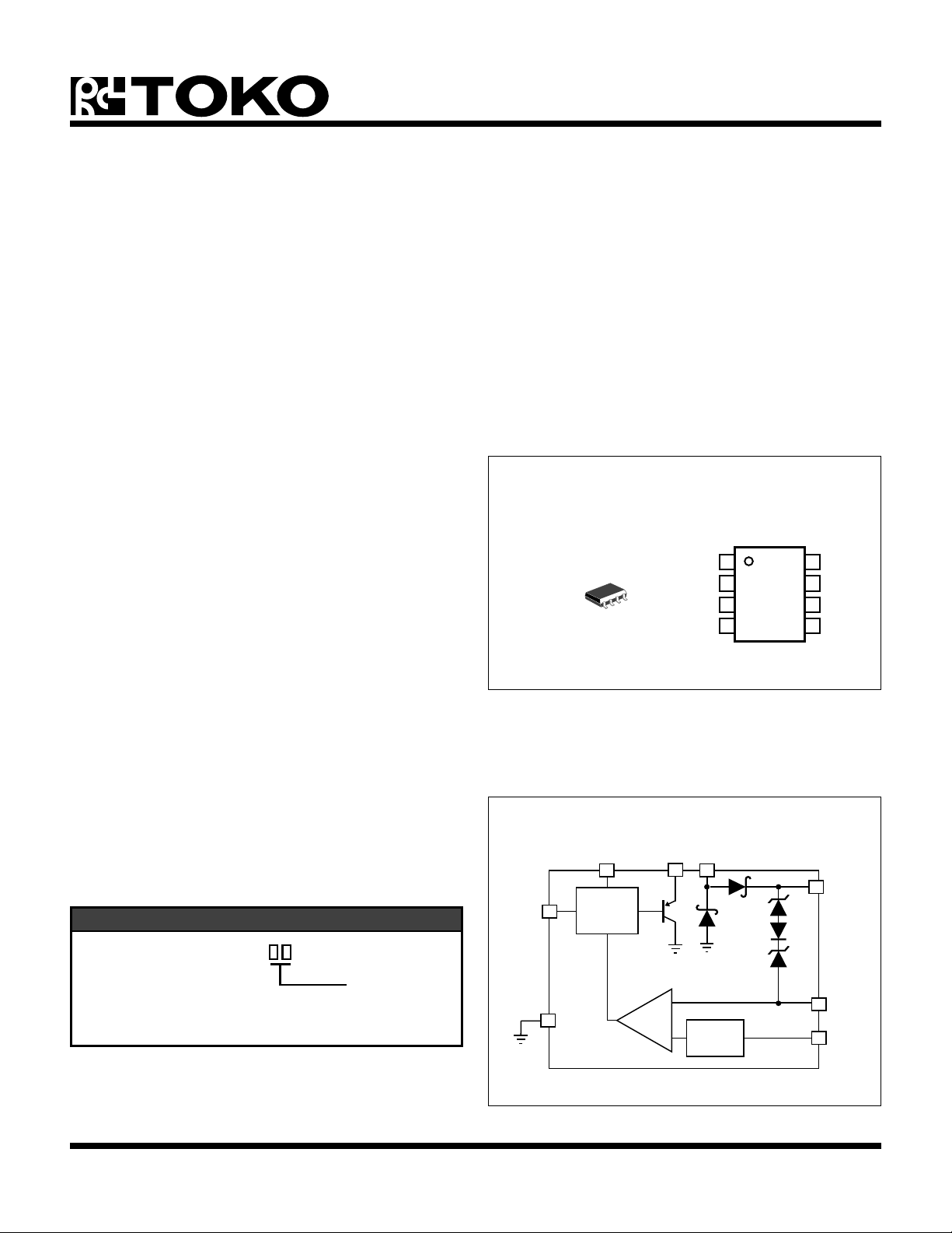
The TK11821 is a low power, low input voltage DC-DC
converter. The device has been optimized for variable
capacitance diode and PIN photodiode bias applications. It
generates 10 Vdc and 24 Vdc output voltages from an input
voltage as low as 0.9 V.
Since the built-in high frequency oscillator generates
sinewaves, the TK11821 produces very low RF interference noise. The internal oscillator is capable of operation
at frequencies as high as 6-8 MHz, therefore, interference
filtering is simple and effective. This unique feature makes
the TK11821 ideally suitable for RF and fiber optic receiver
applications.
APPLICATIONS
■ Variable Capacitance and PIN Photodiode Bias
■ Portable Instrumentation
■ Radio Control Systems
■ Mobile Radios
■ Cellular Telephones
■ Cordless Telephones
■ Fiberoptic Receivers
■ Local Area Network (LAN) Receivers
■ Battery Operated Equipment
TK11821M
1
OSC
2
YPASS
V
V
D
3
4
O
821
A21
8
V
FB
7
GN
V
6
IN
T1
5
The device is capable of operation in the 0.9 to 10 V power
supply voltage range.
The output voltage is 24 V when T1 is not connected. When
T1 is connected to VO, the output voltage is set to 10 V.
The TK11821 is available in an 8-pin plastic surface mount
(MFP-8) package. External inductive components are also
available.
ORDERING INFORMATION
V
6
IN
BLOCK DIAGRAM
V
FB
5
Feedback
Control
OSC
V
D
1
2
V
4
O
TK11821M
Tape/Reel Code
5
ND
7
V REF
TAPE/REEL CODE
BX: Bulk/Bag
TL: Tape Left
MG: Magazine
January, 1996 TOKO, Inc.
1-30-96
T1
3
BYPAS
Page 1
Page 2
TK11821
ABSOLUTE MAXIMUM RATINGS
Input Voltage............................................................ 10 V
Output Voltage ......................................................... 26 V
Output Current ..................................................... 0.5 mA
Operating Voltage Range............................... 0.9 to 10 V
Power Dissipation (Note 1) ................................ 350 mW
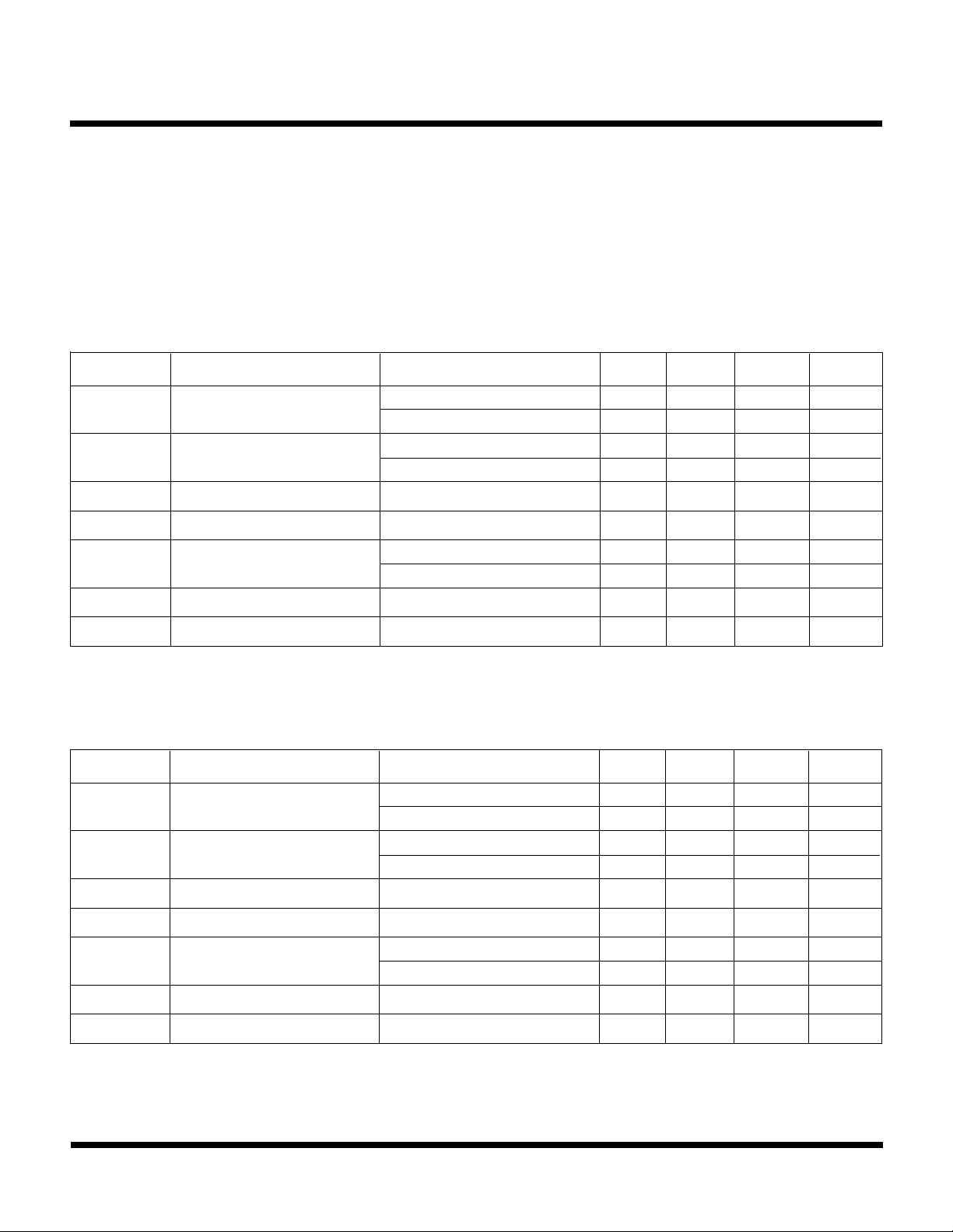
ELECTRICAL CHARACTERISTICS
Test conditions: VIN = 0.9 V → 2.0 V
Operating Conditions: V
SYMBOL PARAMETER TEST CONDITIONS MIN TYP MAX UNITS
I
V
CC
O
Input Current
Output Voltage
= 1.1 V, TA = 25 °C unless otherwise specified.
IN
IO = 0 , VO = 10 V 3.5 7.0 mA
IO = 50 µA, VO = 10 V 5.5 9.0 mA
IO = 0 µA, 1.6 V ≤ VIN ≤ 2.0 V 22.5 24.0 25.5 V
VO - T1 shorted, IO = 50 µA 9.6 10.0 10.4 V
Junction Temperature .......................................... 150 °C
Storage Temperature Range ...................-55 to +150 °C
Operating Temperature Range .................-20 to +70 °C
Lead Soldering Temp. (10 sec.)........................... 260 °C
I
O
Output Current VO - T1 shorted 90 100 µA
Load Reg Load Regulation Note 2 0.1 0.35 %
∆VO/T
V
OSC-S
f
OSC
A
Output Voltage
Temperature Dependency
Oscillation Starting Voltage IO = 0 µA 0.75 V
Oscillation Frequency IO = 0 µA, Note 2 4.0 MHz
VO = 24 V, IO = 50 µA +2.3 mV/°C
VO = 10 V, IO = 50 µA -1.5 mV/°C
ELECTRICAL CHARACTERISTICS
Test conditions: VIN = 1.8 V → 10.0 V
Operating Conditions: V
SYMBOL PARAMETER TEST CONDITIONS MIN TYP MAX UNITS
I
V
I
CC
O
O
Input Current
Output Voltage
Output Current VO - T1 shorted 90 100 µA
Load Reg Load Regulation Note 2 0.1 0.35 %
∆VO/T
A
Output Voltage
Temperature Dependency
= 3.0 V, TA = 25 °C unless otherwise specified.
IN
IO = 0 , VO = 10 V 3.5 7.0 mA
IO = 50 µA, VO = 10 V 5.5 9.0 mA
IO = 0 µA, 1.6 V ≤ VIN ≤ 2.0 V 22.5 24.0 25.5 V
VO - T1 shorted, IO = 50 µA 9.6 10.0 10.4 V
VO = 24 V, IO = 50 µA +2.3 mV/°C
VO = 10 V, IO = 50 µA -1.5 mV/°C
V
OSC-S
f
OSC
Note 1: Power dissipation must be derated at the rate of 3 mW/°C for operation at TA = 25 °C and above.
Note 2: Use the same value for L that was used in the measurement circuit.
Note 3: Output Voltage Variation = (∆V
Note 4: The circuit constants will be changed by the input voltage at the 0.9 V to 2.0 V range and 1.8 V to 10 V range.
Page 2
Oscillation Starting Voltage IO = 0 µA 1.5 V
Oscillation Frequency IO = 0 µA, Note 2 3.5 MHz
O1/VO1
) X 100 (%), ∆V
= VO1 (no load) - V
O1
1-30-96
O1 (IO
= 50 µA).
January, 1996 TOKO, Inc.
Page 3
TK11821
0
3
0
4
0
5
0
1
0
2
0 0.2 0.4 0.6 0.8 1.0
I (mA)
O
0
5
10
V (V)
O
TPC06
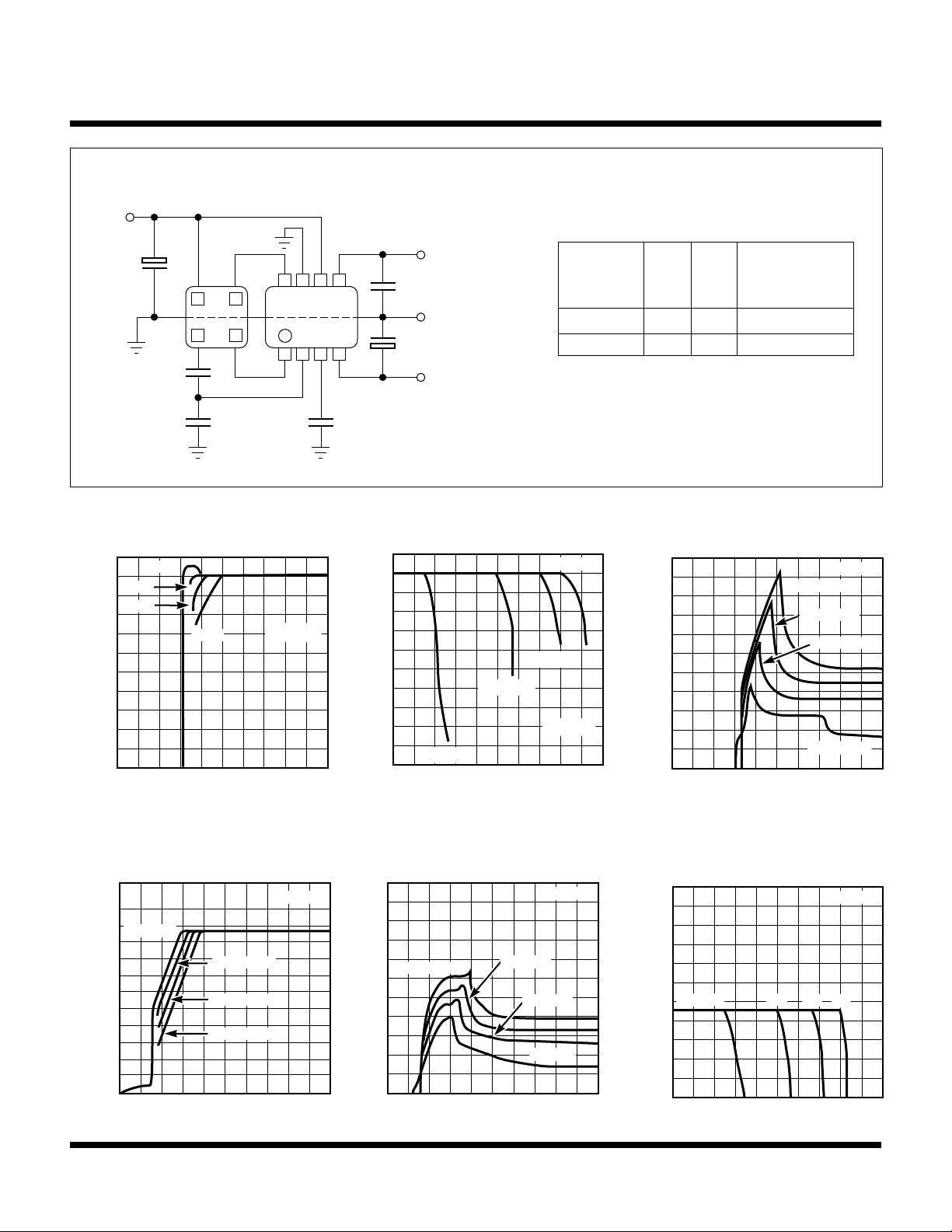
OUTPUT VOLTAGE vs. OUTPUT CURRENT
24 V OUTPUT
T = 25°C
A
V = 2 V
IN
3 V 4 V 5 V
2
TEST CIRCUIT
V
IN
The value of the circuit constants
against the input voltage.
+
2 µF
L
1
3
C
A
C
OUTPUT VOLTAGE vs. INPUT VOLTAGE
10 V OUTPUT
0 µA
40 µA
80 µA
120 µA
O
V (V)
10
5
T
6
4
B
821
C2 0.1 µF
0.1 µF
GND
+
1 µF
V
O
The output voltage is 24 V.
When connected between the V
and the T terminal, the output
voltage will be 10 V.
INPUT TOKO COIL
VOLTAGE C
A CB
0.9 V to 2 V 33 pF 10 pF PS5CDLN-1250
1.8 V to 10 V 820 pF 33 pF PS5CDLN-1303
O
TYPICAL PERFORMANCE CHARACTERISTICS
T = 25 °C
A
OUTPUT VOLTAGE vs. OUTPUT CURRENT
10 V OUTPUT
10
IN
V
= 2 V
O
V (V)
5
V
IN
V = 4 V
= 3 V
IN
INPUT CURRENT vs. INPUT VOLTAGE
10
(mA)
5
IN
I
PART NUMBER
10 V OUTPUT
T = 25°C
A
IO = 120 µA
IO = 80 µA
IO = 40 µA
TA = 25 °C
V
= 1 V
0
0 0.4 0.8 1.2 1.6 2.
V (V)
IN
TPC0
0
OUTPUT VOLTAGE vs. INPUT VOLTAGE
24 V OUTPUT
T = 25 °C
A
24
IO = 0 µA
V (V)
O
10
0
0 0.8 1.6 2.4 3.2 4.
IO = 40 µA
IO = 80 µA
IO = 120 µA
V (V)
IN
TPC0
20
(mA)
10
IN
I
0
0 0.8 1.6 2.4 3.2 4.
January, 1996 TOKO, Inc.
IN
0 0.2 0.4 0.6 0.8 1.
I (mA)
O
TPC0
INPUT CURRENT vs. INPUT VOLTAGE
24 V OUTPUT
T = 25°C
A
1-30-96
V (V)
IN
IO = 80 µA
IO = 40 µA
IO = 0 µA
TPC0
IO = 120 µA
0
0 0.4 0.8 1.2 1.6 2.
V
IO = 0 µA
(V)
IN
TPC0
Page 3
Page 4
TK11821
OUTPUT VOLTAGE vs.
T
VIN
G
1
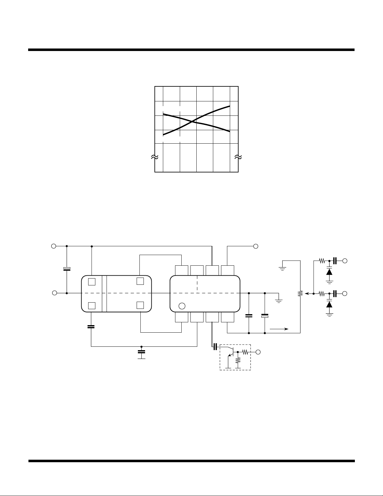
TYPICAL PERFORMANCE CHARACTERISTICS (CONT.)
10.3
10.2
V = 10 V
O
10.1
O
V (V)
10.0
V = 24 V
O
9.9
0
-30 -20 0 20 40 60
TEMPERATURE
TEMP (°C)
TK11821 • TPC07
24.6
24.5
24.4
24.3
24.2
O
V (V)
TYPICAL AM/FM VARACTOR DIODE BIAS CIRCUIT
+
1
ND
C
A
C
B
6
43
1
PIN
821
0.1
+
h
C
2
TR
AM HIGH
FM LOW
TK 11821 BD FIG 0
Page 4
1-30-96
January, 1996 TOKO, Inc.
Page 5
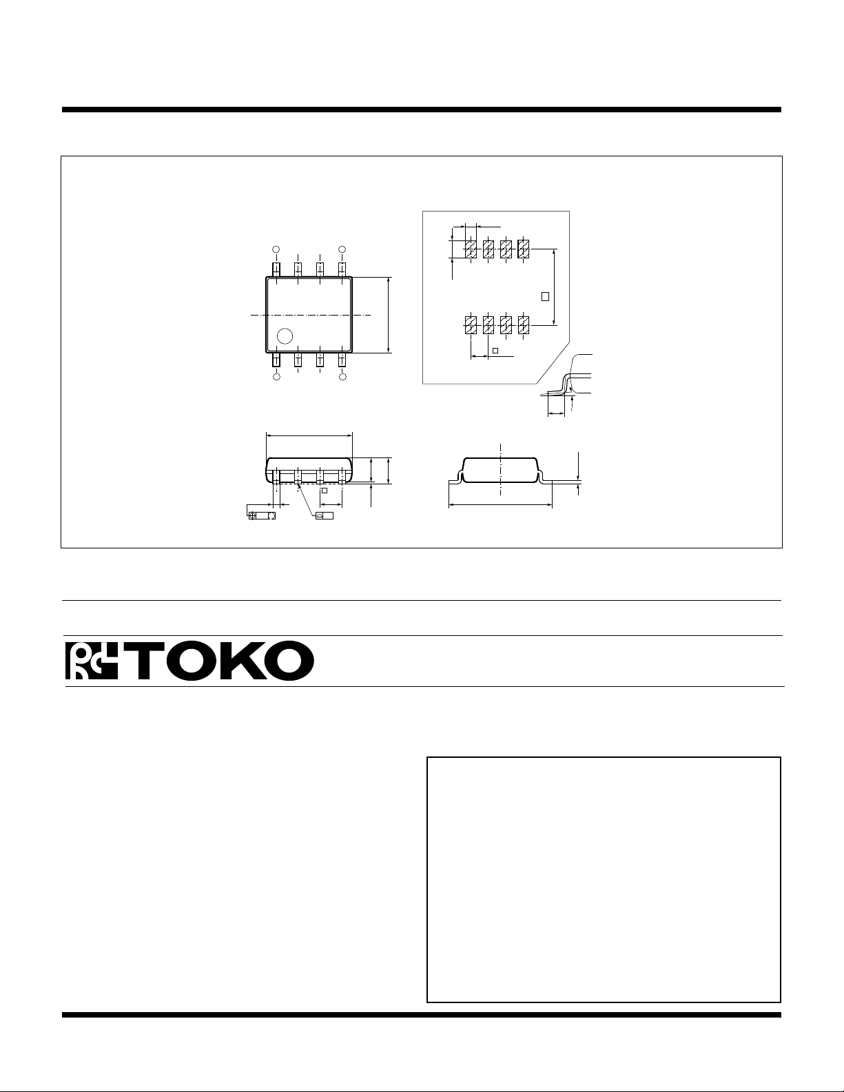
PACKAGE OUTLINES
MFP-8
0.76
TK11821
8
1 4
+0.1
-0.01
0.4
0.12
M
5
1.27
0.2
±
4.4
e
1.27
Recommended Mount Pad
±
0.2
5.0
0.2
±
1.4
0.1min
1.7max
6.0
e
1.27
0.1
5.5
1
e
±
0.2
0.5
0°~10°
-0.05
+0.1
0.15
0.3
±
Unit:mm
Marking Information
821
The information furnished by TOKO, Inc. is believed to be accurate and reliable. However, TOKO reserves the right to make changes or improvements in the design, specification or manufacture of its products without further notice. TOKO
does not assume any liability arising from the application or use of any product or circuit described herein, nor for any infringements of patents or other rights of third parties which may result from the use of its products. No license is granted
by implication or otherwise under any patent or patent rights of TOKO, Inc.
TOKO America, Inc.
1250 Feehanville Dr.
Mt. Prospect, IL 60056
Tel: (800) PIK-TOKO
Fax: (847) 699-1194
January, 1996 TOKO, Inc.
© 1993 Toko America, Inc.
All Rights Reserved
YOUR LOCAL REPRESENTATIVE IS:
1-30-96
Order this literature by: IC-109-TK11821
Page 5
Printed in U.S.A.
 Loading...