

Page 1
TK14584
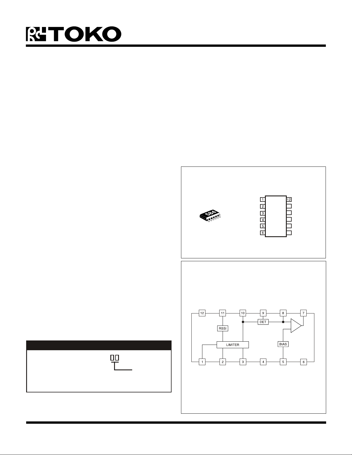
GND
RSSI
IF OUTPUT
DET INPUT
DET OUTPUT
AMP OUTPUT
IF INPUT
DECOUPLE
DECOUPLE
NC
POWER SAVE
V
CC
+
-
GND
AMP
V
CC
FM IF IC
FEATURES
■ Input Frequency (~22 MHz)
■ Low Voltage Operation (2.3 to 5.5 V)
■ Battery Save Function
■ Wide Band Demodulator (~1 MHz)
■ Very Small Package (SSOP-12)
DESCRIPTION
The TK14584M is a standard function general purpose IF
IC capable of operating up to 22 MHz. The TK14584M has
a unique function that allows establishing the demodulation
characteristics by changing the external RC time constant,
and not changing the phase shifter constant. The RSSI
output is individually trimmed, resulting in excellent
accuracy, good linearity, and stable temperature
characteristics. The TK14584M was developed for highspeed data communication, DECT, wireless LAN, keyless
entry systems, etc.
APPLICATIONS
■ Communications Equipment
■ Wireless LAN
■ Keyless Entry Systems
TK14584M
IF INPUT
DECOUPLE
DECOUPLE
NC
POWER SAVE
V
CC
BLOCK DIAGRAM
GND
RSSI
11
10
IF OUTPUT
DET INPUT
9
8
DET OUTPUT
AMP OUTPUT
7
The TK14584M is available in the very small SSOP-12
surface mount package.
ORDERING INFORMATION
TK14584M
January 2000 TOKO, Inc. Page 1
Tape/Reel Code
TAPE/REEL CODE
TL: Tape Left
Page 2
TK14584
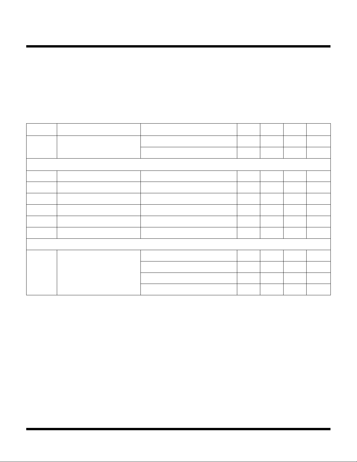
ABSOLUTE MAXIMUM RATINGS
Supply Voltage ........................................................... 6 V
Operating Voltage Range.............................. 2.3 to 5.5 V
Power Dissipation (Note 1) ................................ 250 mW
TK14584M ELECTRICAL CHARACTERISTICS
Test conditions: V
LOBMYSRETEMARAPSNOITIDNOCTSETNIMPYTXAMSTINU
CC
= 3 V, f
= 10.7 MHz, fm = 1 kHz, Modulation = ±50 kHz, T
IN
Storage Temperature Range ................... -55 to +150 °C
Operating Temperature Range ...................-30 to +85 °C
Operating Frequency Range (IF) ................. 6 to 22 MHz
Operating Frequecy Range (Demodulation) ..... to 1 MHz
= 25 °C, unless otherwise specified.
A
I
CC
tnerruCylppuS
tupnioN,NO=evaSrewoP2.00.5Aµ
FI
tupnioN5.30.5Am
V
TUO
egatloVtuptuOtupnimBd03-021002063smrVm
DHTnoitrotsiDcinomraHlatoTtupnimBd03-5.00.2%
N/SoitaResioNotlangiStupnimBd03-0607Bd
DANISDANISBd21 98-38-mBd
R
)NI(FI
ecnatsiseRtupnIretimiL 4.18.12.2kΩ
GniaG9657Bd
ISSR
tupnioN00.002.003.0V
tupnidetaludom-nonmBd06-04.055.007.0V
V
ISSR
egatloVtuptuOISSR
tupnidetaludom-nonmBd03-50.102.104.1V
tupnidetaludom-nonmBd005.107.159.1V
Note 1: Power dissipation is 250 mW when mounted as recommended. Derate at 2.0 mW/°C for operation above 25°C.
Page 2 January 2000 TOKO, Inc.
Page 3
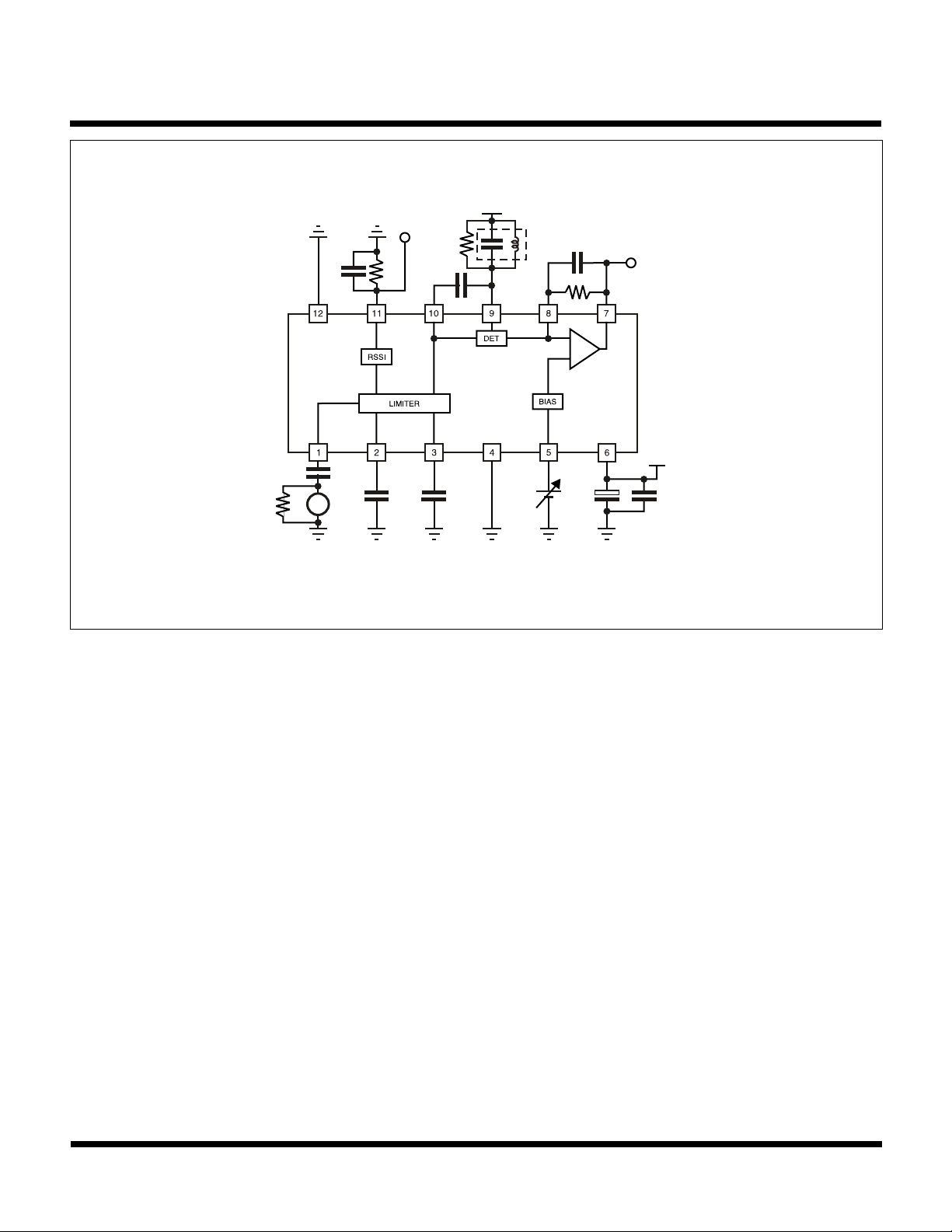
0.01 µF
TEST CIRCUIT
V
12 kΩ
RSSI
OUT
3.3 kΩ
CC
836BH-0268 (TOKO)
1000 pF
TK14584
DET OUTPUT
50 Ω
GND
~
0.01 µF
IF-INPUT
1 pF
0.01 µF 0.01 µF
51 kΩ
+
AMP
P.S.
4.7 µF 0.01 µF
V
CC
V
CC
+
January 2000 TOKO, Inc. Page 3
Page 4
TK14584
(
)
(
)
(
)
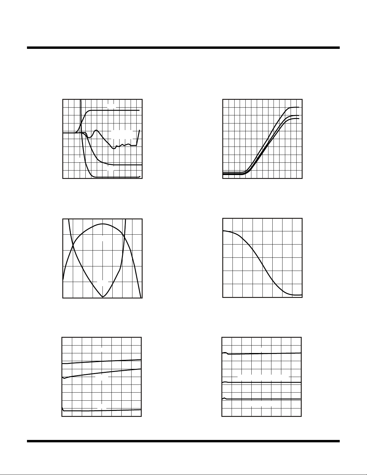
TYPICAL PERFORMANCE CHARACTERISTICS
TA = 25 °C, unless otherwise specified.
S+N, N, AM OUT, TOTAL
HARMONIC DISTORTION vs.
0
INPUT VOLTAGE
S+N
-20
-40
AM OUT
(30% mod.)
-60
S+N,N, AM OUT (dBV)
-80
THD
N
-100
-120 -100 -80 -60 -40 -20 0 20
VIN (dBm)
DETUNE CHARACTERISTICS
-10
-20
V
OUT
-30
(dBV)
-40
OUT
V
20
16
12
8
4
0
20
16
12
8
%
THD
%
THD
RSSI OUTPUT VOLTAGE vs.
INPUT VOLTAGE
2.0
1.6
1.2
(V)
RSSI
0.8
V
0.4
0.0
-120 -100 -80 -60 -40 -20 0 20
VIN (dBm)
S CURVE
3
2
(V)
OUT(DC)
1
V
V
CC
5.5 V
3.0 V
2.3 V
-50
-60
10.3 10.5 10.7 10.9 11.1
THD
fIN (MHz)
SUPPLY CURRENT, OUTPUT VOLTAGE,
TOTAL HARMONIC DISTORTION vs.
SUPPLY VOLTAGE
300
I
260
CC
220
V
(mVrms)
180
OUT
V
140
100
2 3 4 5 6
OUT
THD
VCC (V)
4
0
5
4
3
2
1
0
(mA)
CC
THD (dB), I
0
10.3 10.5 10.7 10.9 11.1
fIN (MHz)
SIGNAL TO NOISE RATIO,
-3 dB LIMITING SENSITIVITY,
12 dB SINAD vs. SUPPLY VOLTAGE
80
70
S/N
60
-3 dB LIMITING SENSITIVITY
S/N (dB)
50
40
30
2 3 4 5 6
12 dB SINAD
VCC (V)
-50
-60
-70
dBm
-80
-90
12 dB SINAD
-3 dB LIMITING SENSITIVITY,
-100
Page 4 January 2000 TOKO, Inc.
Page 5
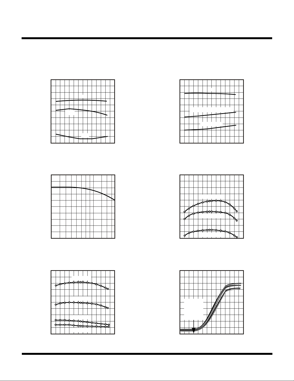
TYPICAL PERFORMANCE CHARACTERISTICS (CONT.)
(
)
TA = 25 °C, unless otherwise specified.
TK14584
SUPPLY CURRENT, OUTPUT VOLTAGE,
TOTAL HARMONIC DISTORTION
vs. TEMPERATURE
300
260
I
CC
220
V
(mVrms)
180
OUT
V
OUT
140
THD
100
-40 -20 0 20 40 60 80 100
TA (°C)
LIMITER GAIN vs.
INPUT FREQUENCY
100
80
60
5
4
3
2
1
0
(mA)
CC
THD (%), I
SIGNAL TO NOISE RATIO,
-3 dB LIMITING SENSITIVITY,
12 dB SINAD vs. TEMPERATURE
80
70
S/N
60
-3 dB LIMITING SENSITIVITY
S/N (dB)
50
12 dB SINAD
40
30
-40 -20 0 20 40 60 80 100
TA (°C)
RSSI OUTPUT VOLTAGE vs.
TEMPERATURE
2.0
1.8
VIN = 0 dBm
(V)
1.6
-50
-60
-70
dBm
-80
-90
12 dB SINAD
-3 dB LIMITING SENSITIVITY,
-100
40
GAIN (dB)
20
0
1 3 5 10 30 50
fIN (MHz)
RSSI OUTPUT VOLTAGE vs.
TEMPERATURE
1.0
VIN = -45 dBm
0.8
0.6
(V)
RSSI
0.4
V
0.2
0.0
-40 -20 0 20 40 60 80 100
VIN = -60 dBm
VIN = -75 dBm
VIN = -90 dBm
TA (°C)
RSSI
1.4
V
VIN = -15 dBm
1.2
1.0
VIN = -30 dBm
-40 -20 0 20 40 60 80 100
TA (°C)
RSSI OUTPUT VOLTAGE vs.
INPUT VOLTAGE
2.0
1.6
1.2
(V)
RSSI
V
TEMP (deg)
-30
0.8
0.4
0.0
-120 -100 -80 -60 -40 -20 0 20
0
25
50
70
85
VIN (dBm)
January 2000 TOKO, Inc. Page 5
Page 6
TK14584
(
)
(
)
(
)
3
2
(V)
OUT(DC)
1
V
0
9.9 10.3 10.7 11.1 11.5
TYPICAL PERFORMANCE CHARACTERISTICS (CONT.)
TA = 25 °C, unless otherwise specified.
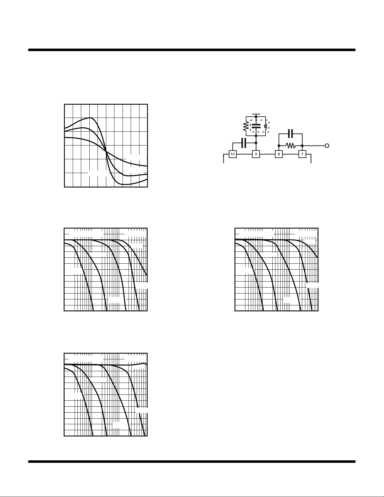
S CURVE
V
CC
836BH-0268 (TOKO)
RD = 3.3 k
fIN (MHz)
RD
1 pF
RD = 1.0 k
RD = 2.0 k
C
51 kΩ
DET OUTPUT
OUTPUT VOLTAGE vs.
MODULATING FREQUENCY
2
0 dB = 208 mVrms
RD = 3.3 kΩ
0
(dB)
OUT
V
-2
-4
C = 1000 pF
-6
C = 330 pF
-8
-10
-12
1 3 10 30 100 300 1000
C = 47 pF
MODULATING FREQUENCY fm
OUTPUT VOLTAGE vs.
MODULATING FREQUENCY
2
0 dB = 35.2 mVrms
RD = 1.0 kΩ
0
(dB)
OUT
V
-2
-4
C = 1000 pF
-6
C = 330 pF
-8
C = ∞
C = 10 pF
C = ∞
C = 10 pF
kHz
OUTPUT VOLTAGE vs.
MODULATING FREQUENCY
2
0 dB = 107 mVrms
RD = 2.0 kΩ
0
(dB)
OUT
V
-2
-4
C = 1000 pF
-6
C = 330 pF
-8
-10
-12
1 3 10 30 100 300 1000
C = 47 pF
MODULATING FREQUENCY fm
C = ∞
C = 10 pF
kHz
-10
-12
1 3 10 30 100 300 1000
MODULATING FREQUENCY fm
C = 47 pF
kHz
Page 6 January 2000 TOKO, Inc.
Page 7
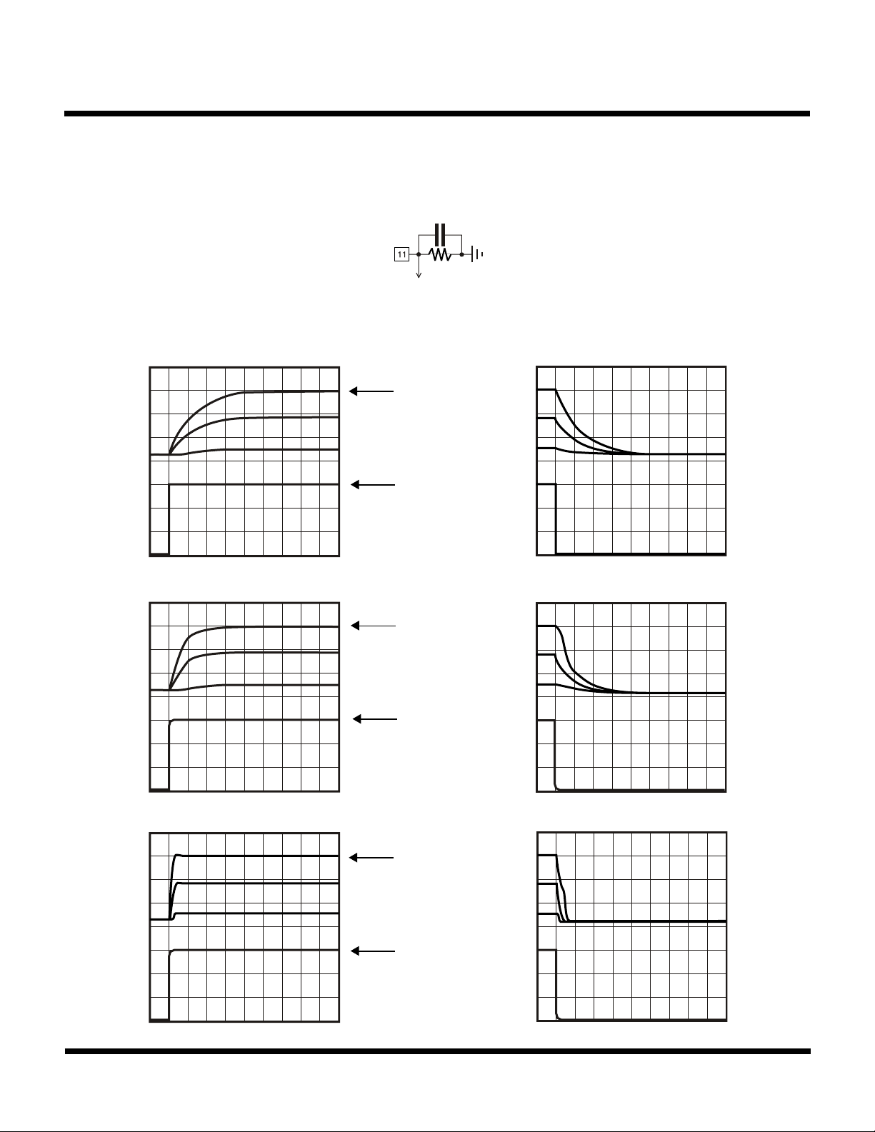
TYPICAL PERFORMANCE CHARACTERISTICS (CONT.)
TA = 25 °C, unless otherwise specified.
RSSI Output Voltage Transient Response (IF Input ON/OFF)
C
IF INPUT VOLTAGE
= -10, -40, -70 dBm
C = 0.01 µF
12 k
RSSI OUTPUT
RSSI OUTPUT
-10 dBm in
-40 dBm in
-70 dBm in
(0.5V/div)
SG
GATE PULSE
(1V/div)
TK14584
C = 0.001 µF
C = 0.0001 µF
0.1 ms/div
RSSI OUTPUT
-10 dBm in
-40 dBm in
-70 dBm in
(0.5V/div)
SG
GATE PULSE
(1V/div)
20 µs/div 20 µs/div
RSSI OUTPUT
-10 dBm in
-40 dBm in
-70 dBm in
(0.5V/div)
SG
GATE PULSE
(1V/div)
0.1 ms/div
20 µs/div
20 µs/div
January 2000 TOKO, Inc. Page 7
Page 8
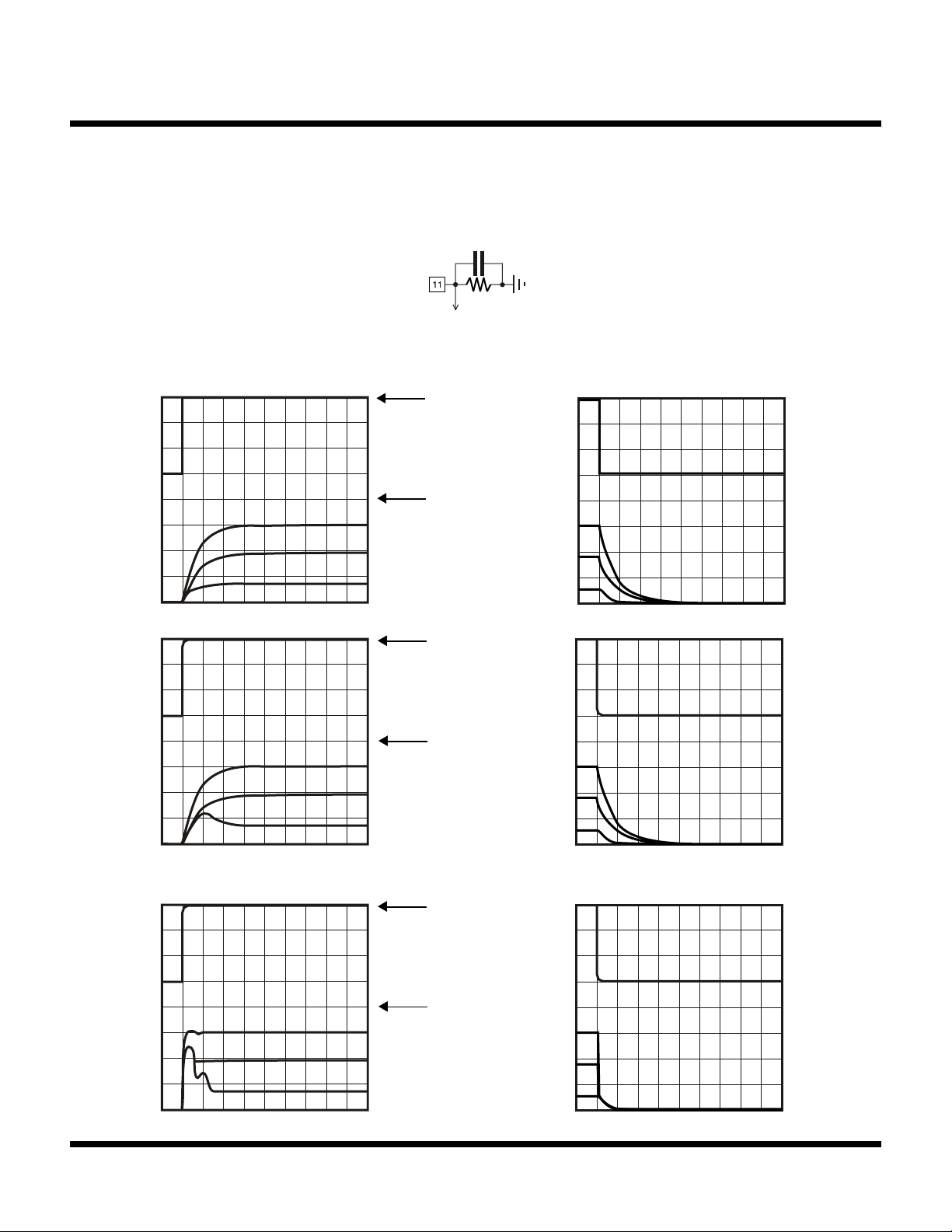
TK14584
TYPICAL PERFORMANCE CHARACTERISTICS (CONT.)
TA = 25 °C, unless otherwise specified.
RSSI Output Voltage Transient Response (Power Save ON/OFF)
C
IF INPUT VOLTAGE
= -10, -40, -70 dBm
12 k
RSSI OUTPUT
C = 0.01 µF
C = 0.001 µF
POWER SAVE
(1V/div)
RSSI OUTPUT
-10 dBm in
-40 dBm in
-70 dBm in
(0.5V/div)
0.2 ms/div
POWER SAVE
(1V/div)
RSSI OUTPUT
-10 dBm in
-40 dBm in
-70 dBm in
(0.5V/div)
20 µs/div 20 µs/div
0.2 ms/div
C = 0.0001 µF
20 µs/div 20 µs/div
POWER SAVE
(1V/div)
RSSI OUTPUT
-10 dBm in
-40 dBm in
-70 dBm in
(0.5V/div)
Page 8 January 2000 TOKO, Inc.
Page 9
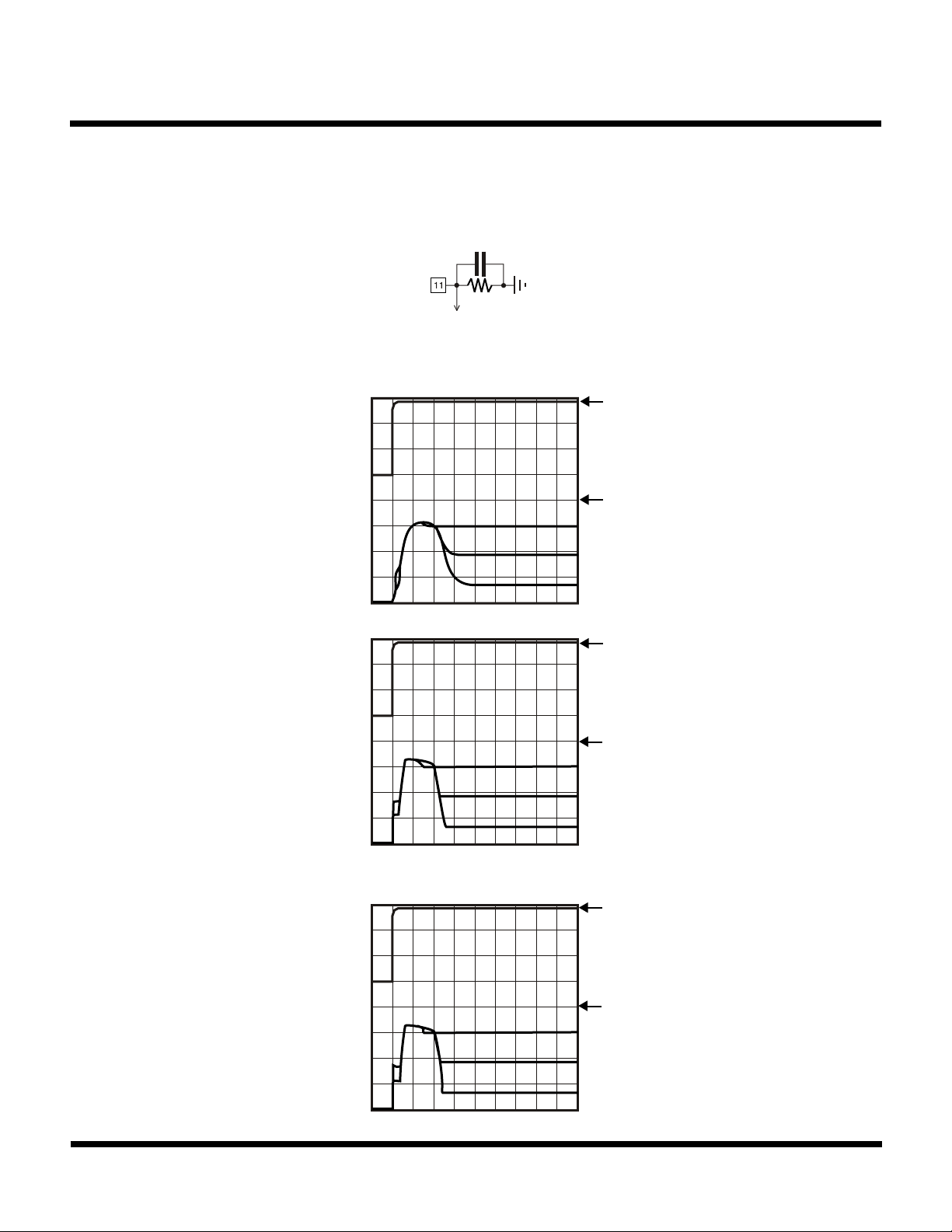
TYPICAL PERFORMANCE CHARACTERISTICS (CONT.)
TA = 25 °C, unless otherwise specified.
RSSI Output Voltage Transient Response (Supply Voltage ON)
C
IF INPUT VOLTAGE
= -10, -40, -70 dBm
12 k
RSSI OUTPUT
TK14584
C = 0.01 µF
C = 0.001 µF
0.5 ms/div
0.5 ms/div
V
CC
(1V/div)
RSSI OUTPUT
-10 dBm in
-40 dBm in
-70 dBm in
(0.5V/div)
V
CC
(1V/div)
RSSI OUTPUT
-10 dBm in
-40 dBm in
-70 dBm in
(0.5V/div)
C = 0.0001 µF
V
CC
(1V/div)
RSSI OUTPUT
-10 dBm in
-40 dBm in
-70 dBm in
(0.5V/div)
0.5 ms/div
January 2000 TOKO, Inc. Page 9
Page 10
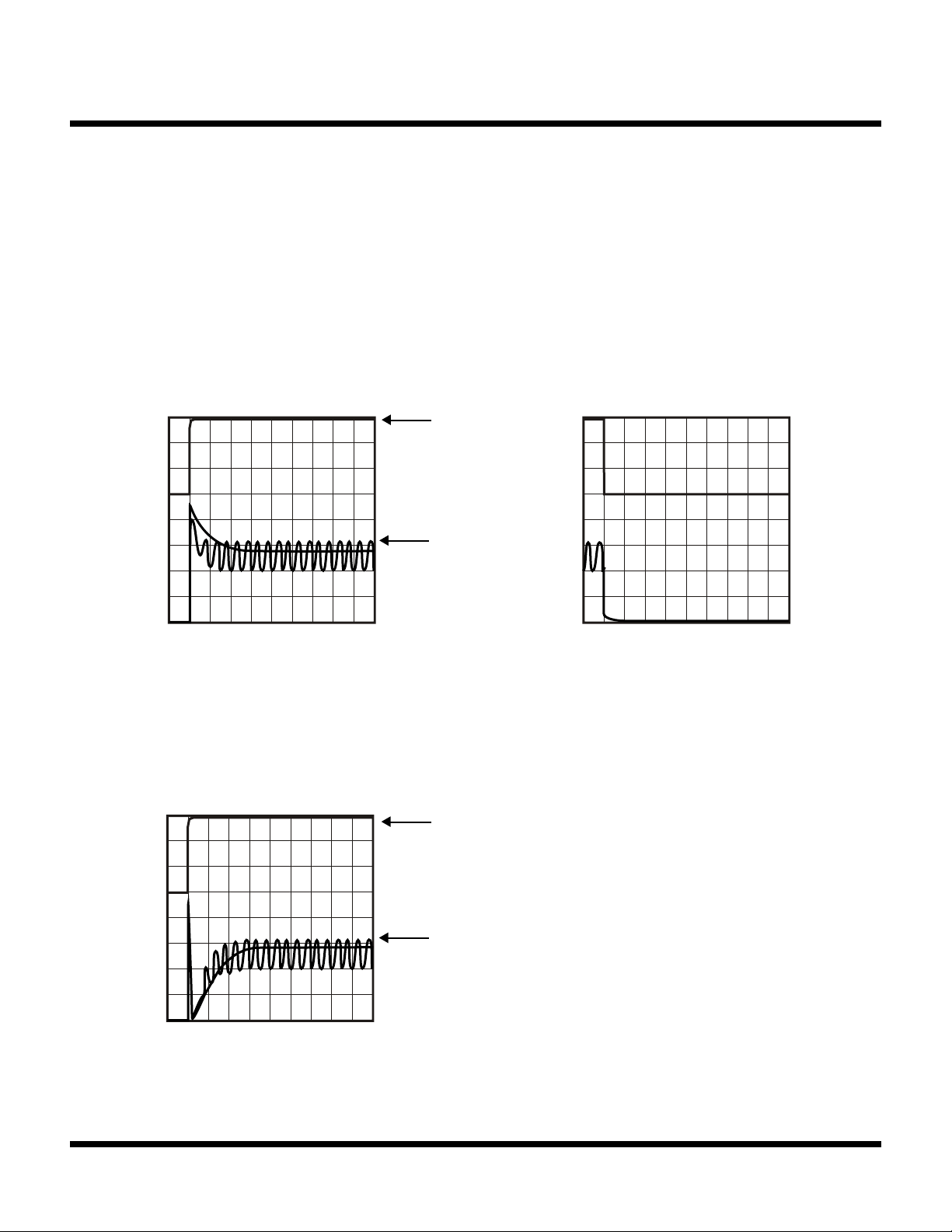
TK14584
TYPICAL PERFORMANCE CHARACTERISTICS (CONT.)
TA = 25 °C, unless otherwise specified.
Detector Output Voltage Transient Response (Power Save ON/OFF,Supply Voltage ON)
IF INPUT VOLTAGE
= -40 dBm, No input
POWER SAVE ON/OFF
POWER SAVE
(1V/div)
DET OUTPUT
SUPPLY VOLTAGE ON
2 ms/div
-40 dBm in,
No input
(0.5V/div)
V
CC
(1V/div)
DET OUTPUT
-40 dBm in,
No input
(0.5V/div)
2 ms/div
2 ms/div
Page 10 January 2000 TOKO, Inc.
Page 11
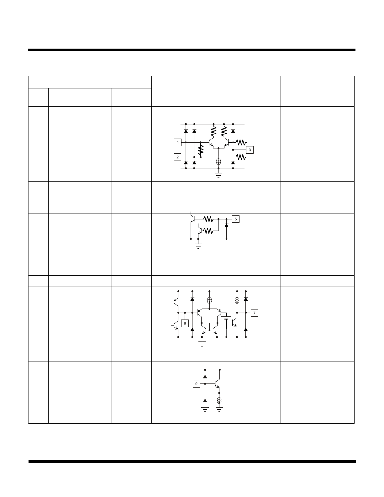
PIN FUNCTION DESCRIPTION
V
CC
1.2 V
LANIMRET
NIP
.ON
LOBMYSEGATLOV
TK14584
TIUCRICTNELAVIUQELANRETNINOITPIRCSED
1
2
3
TUPNIFI
ELPUOCED
ELPUOCED
V9.1
V9.1
V9.1
1.8 k
100 k
100 k
V
CC
4CN .noitcennoclanretnioN
5EVASREWOPV
6V
7
8
CC
TUPTUOPMA
TUPTUOTED
S
100 k
100 k
V0.3
V2.1
V2.1
TUPNIpmAgnitimiL:1
pmAgnitimiL:3,2
gnilpuoceD
tsumnipsiht,revewoH
DNGotdetcennoceb
.noitcuderesionrof
:nOevaSrewoP
V
S
V3.0<
:ffOevaSrewoP
V
S
VotV5.1=
CC
tuptuOreifilpmA:7
tuptuOrotceteD:8
9TUPNITEDV0.3tupnIrotceteD
V
CC
January 2000 TOKO, Inc. Page 11
Page 12
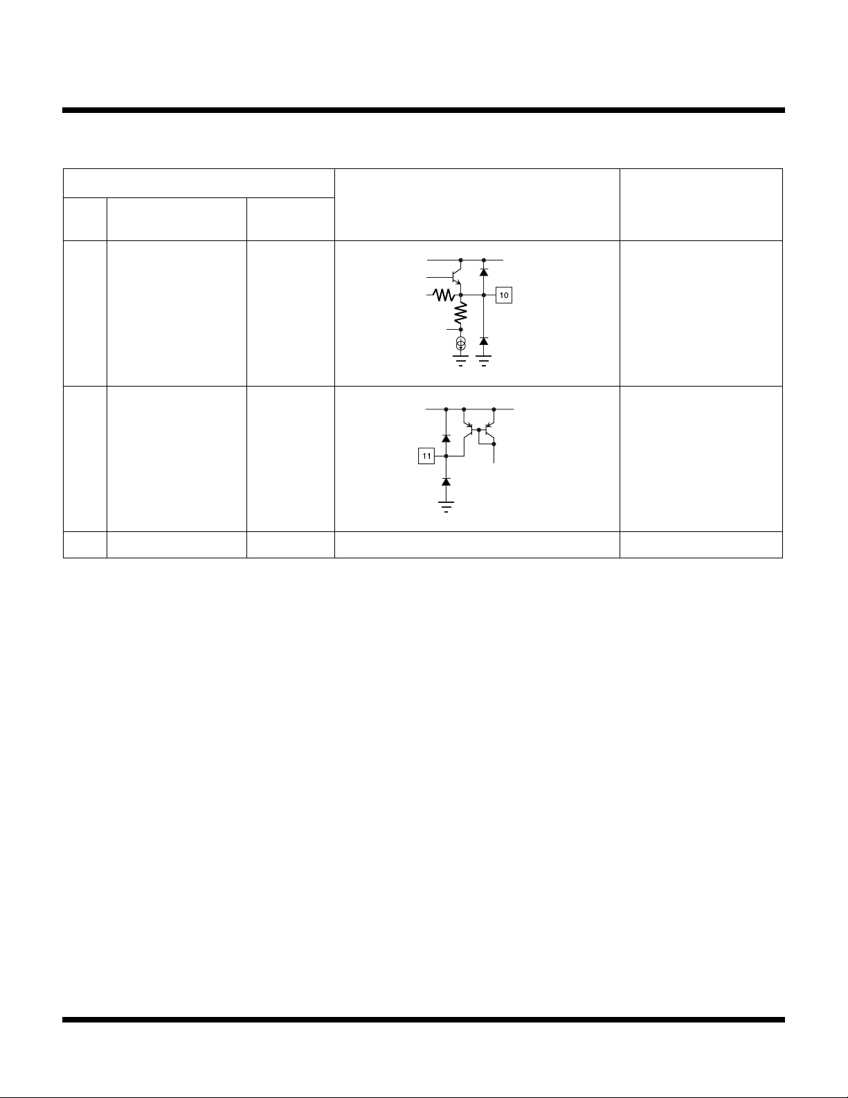
TK14584
PIN FUNCTION DESCRIPTION
LANIMRET
NIP
.ON
LOBMYSEGATLOV
TIUCRICTNELAVIUQELANRETNINOITPIRCSED
01TUPTUOFIV9.1tuptuOretimiLFI
100 k
11ISSR tuptuOISSR
V
CC
V
CC
21DNGV0
Page 12 January 2000 TOKO, Inc.
Page 13
GND
RSSI
IF OUTPUT
DET INPUT
DET OUTPUT
AMP OUTPUT
IF INPUT
DECOUPLE
DECOUPLE
NC
POWER SAVE
V
CC
+
-
GND
AMP
V
CC
CIRCUIT DESCRIPTION
TK14584
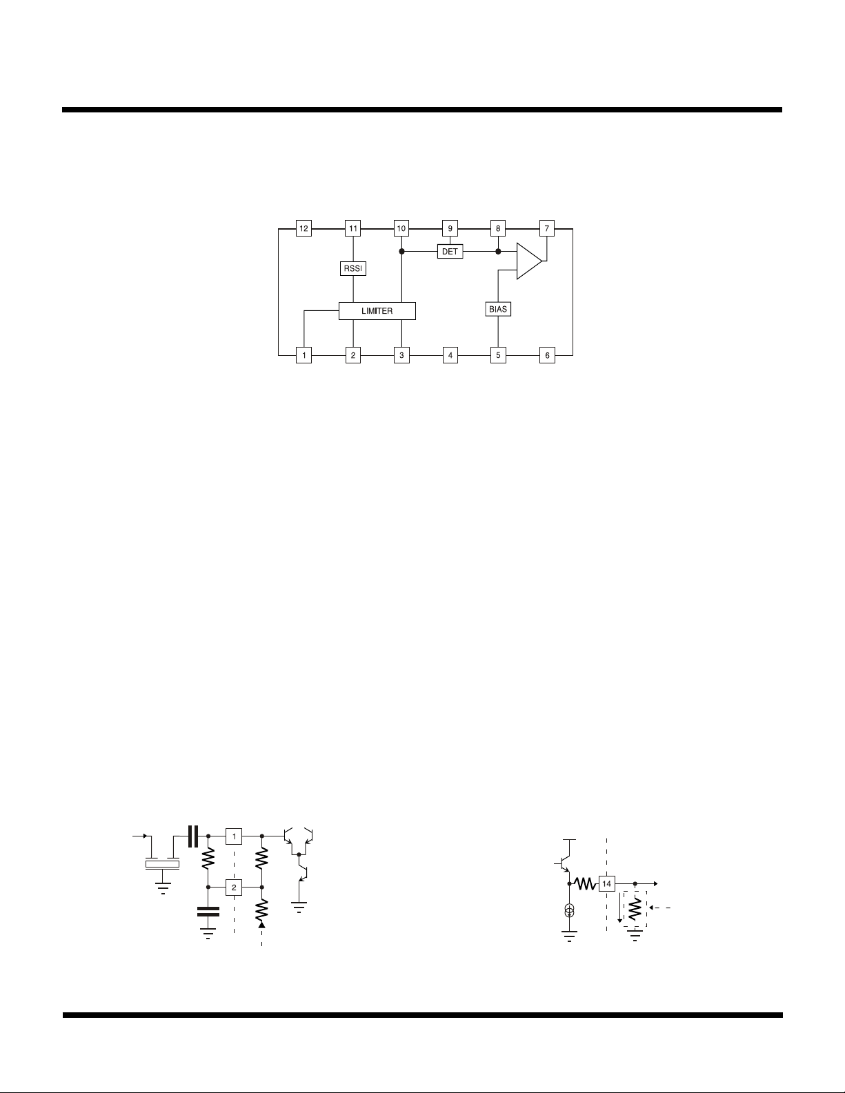
IF Limiter Amplifier, RSSI:
The IF limiter amplifier is composed of five differential gain stages. The total gain of the IF limiter amplifier is 80 dB. The
output signal of the IF limiter amplifier is provided at Pin 10 through the emitter-follower output stage. The IF limiter amplifier
output level is 0.5 V
P-P
.
The input resistance of the IF limiter amplifier is 1.8 kΩ (see Figure 1A). If the impedance of the filter is lower than 1.8
kΩ, connect an external resistor between Pin 1 and Pin 2 in parallel to provide the equivalent load impedance of the filter.
Figure 1A shows the case that the impedance of the filter is 330 Ω.
The operating current of the emitter-follower of the IF limiter amplifier output is 200 µA. If the capacitive load is large, the
negative half cycle of the output waveform may be distorted. This distortion can be reduced by connecting an external
resistor between Pin 10 to GND to increase the operating current. The increased operating current from an external resistor
is calculated as follows (see Figure 1B):
The increased operating current Ie (mA) = (VCC - 1.0) / Re (kΩ)
V
CC
1.8 K
100 kΩ
200 µA
IF OUTPUT
I
e
R
e
330
FIGURE 1A
January 2000 TOKO, Inc. Page 13
FIGURE 1B
Page 14
TK14584
CIRCUIT DESCRIPTION (CONT.)
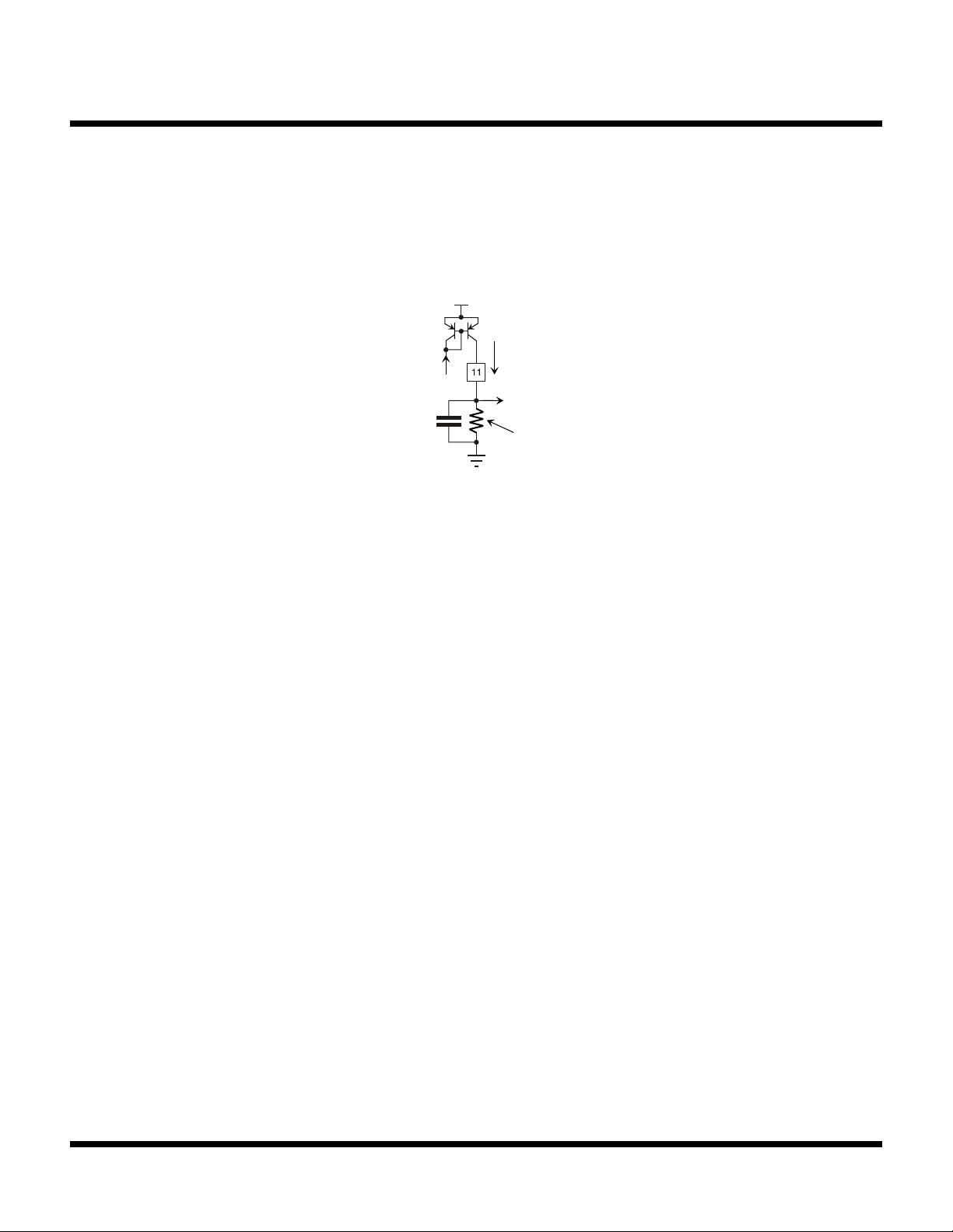
The RSSI output is a current output. It converts to a voltage by an external resistor between Pin 11 and GND. The time
constant of the RSSI output is determined by the product of the external converting resistance and parallel capacitance.
When the time constant is longer, the RSSI output is less likely to be influenced by a disturbance or component of amplitude
modulation, but the RSSI output response is slower. The external resistance and capacitance are determined by the
application.
V
CC
OUTPUT
CURRENT
RSSI- OUT
Current-to-Voltage
Transformation Resistor
FIGURE 2 - RSSI OUTPUT STAGE
The slope of the RSSI curve characteristic can be modified by changing the external resistance. In this case, the maximum
range of converted RSSI output voltage is GND level to about V
- 0.2 V (the supply voltage minus the collector saturation
CC
voltage of the output transistor).
In addition, the temperature characteristic of the RSSI output voltage can be modified by changing the temperature
characteristic of the external resistor. Normally, the temperature characteristic of the RSSI output voltage is very stable
when using a carbon resistor or metal film resistor with a temperature characteristic of 0 to 200 ppm/ °C.
The RSSI output is trimmed individually for enhanced accuracy.
AM Demodulation by Using the RSSI Output:
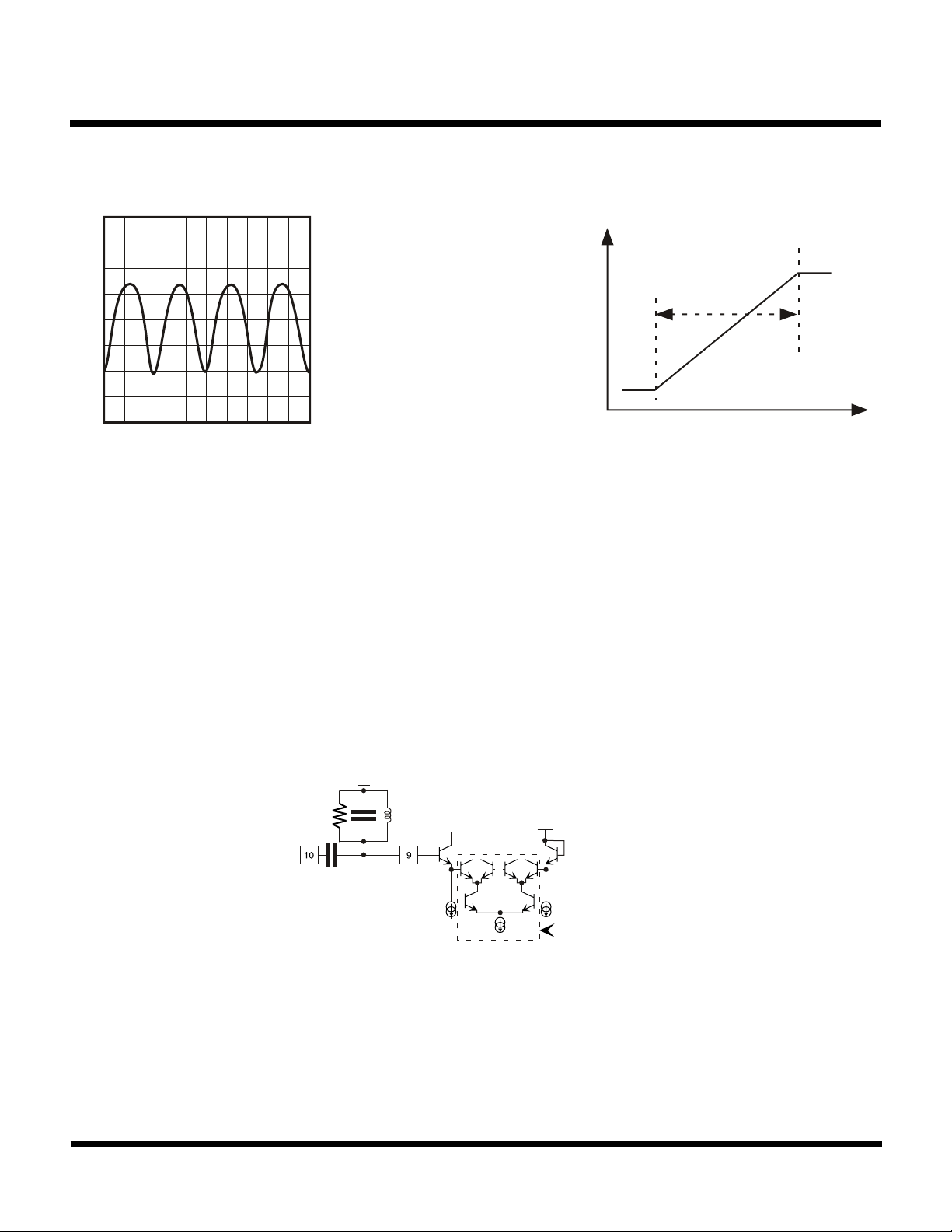
Although the distortion of the RSSI output is high because it is a logarithmic detection of the IF input envelope, AM can
be demodulated simply by using the RSSI output. In this case, the input dynamic range that can demodulate AM is the
inside of the linear portion of the RSSI curve characteristic (see Figure 3B).
This method does not have a feedback loop to control the gain because an AGC amplifier is not necessary (unlike the
popularly used AM demodulation method). Therefore, it is a very useful for some applications because it does not have
the response time problem.
Figure 3A shows the AM demodulated waveform.
Page 14 January 2000 TOKO, Inc.
Page 15
CIRCUIT DESCRIPTION (CONT.)
Operating Condition
VCC = 3 V, fIN = 10.7 MHz,
fm = 40 kHz, Mod = 80%,
VIN = -40 dBm
100mV/div
10µs/div
TK14584
RSSI-OUT (V)
AM can be
demodulated
inside of linear
range
RF INPUT - LEVEL (dBu)
FIGURE 3A - AM DEMODULATED WAVEFORM
FIGURE 3B
FM Detector:
The FM detector is included in the quadrature FM detector using a Gilbert multiplier.
It is suitable for high speed data communication because the demodulation bandwidth is over 1 MHz.
The phase shifter is connected between Pin 10 (IF limiter output) and Pin 9 (input detector). Any available phase shifter
can be used: a LC resonance circuit, a ceramic discriminator, a delay line, etc.
Figure 4 shows the internal equivalent circuit of the detector.
V
CC
V
CC
QB
QA
V
CC
multiplier core circuit
FIGURE 4
January 2000 TOKO, Inc. Page 15
Page 16
TK14584
CIRCUIT DESCRIPTION (CONT.)
The signal from the phase shifter is applied to the multiplier (in the dotted line) through emitter-follower stage QA. When
the phase shifter is connected between Pin 10 and Pin 9, note that the bias voltage to Pin 9 should be provided from an
external source because Pin 9 is only connected to the base of QA.
Because the base of QB (at the opposite side) is connected with the supply voltage, Pin 9 has to be biased with the
equivalent voltage.
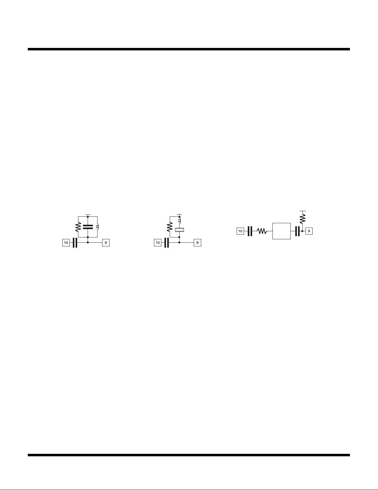
Using an LC resonance circuit is not a problem (see Figure 5). However, when using a ceramic discriminator, it is necessary
to pay attention to bias. If there is a difference of the base voltages, the DC voltages of the multiplier do not balance. It
alters the DC zero point or worsens the distortion of demodulation output.
The Pin 9 input level should be saturated at the multiplier; if this level is lower, it is easy to disperse the modulation output.
Therefore, to have stable operation, Pin 9 should be higher than 100 mV
The following figures show examples of the phase shifter.
P-P
.
Rz is the characteristic impedance
V
CC
LC resonance circuit ceramic discriminator delay line
V
CC
Rz
Delay
Line
Rz
V
CC
FIGURE 5 - EXAMPLES OF PHASE SHIFTERS
Establishing Demodulation Characteristics:
Generally, demodulation characteristics of FM detectors are determined by the external phase shifter. However, this
product has a unique function which can optionally establish the demodulation characteristics by the time constant of the
circuit parts after demodulation. The following explains this concept.
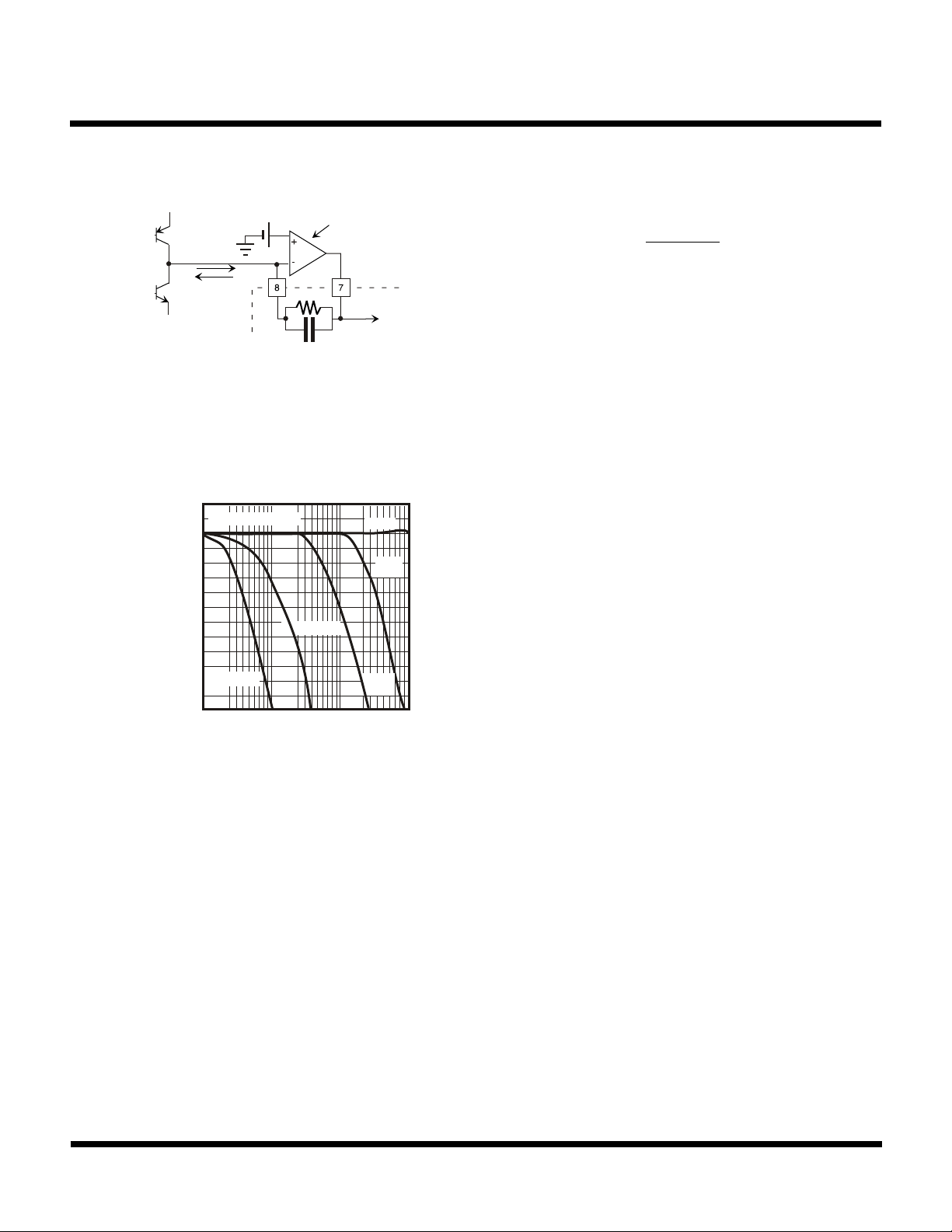
Figure 6 shows the internal equivalent circuit of the detector output stage.
The multiplier output current of the detector is converted to a voltage by the internal OP AMP. The characteristic of this
stage is determined by converting the current to voltage with resistor RO and the capacitor CO connected between Pin 7
and Pin 8 (see Figure 6).
In other words, the slope of the S-curve characteristic can be established optionally with resistor RO without changing the
constant of the phase shifter. The demodulated bandwidth can be established optionally by the time constant of this
external resistor RO and capacitor CO inside of a bandwidth of the IF-filter and phase shifter. Figure 7 shows an example
of this characteristic.
Page 16 January 2000 TOKO, Inc.
Page 17
CIRCUIT DESCRIPTION (CONT.)
(Hz)
TK14584
The -3 dB frequency Fc is calculated by the following:
2 π C
1
0R0
Fc =
The S-curve output voltage is calculated by the following
as centering around the internal reference voltage V
V
= V
± io X R
ref
Where V
= 1.4 V, maximum of current io = ±100 µA
ref
OUT
io
Demodulated
Output Current
V
ref
I to V convertor
R
0
C
0
Demodulated
Output Voltage
V
OUT
FIGURE 6 - INTERNAL EQUIVALENT CIRCUIT OF DETECTOR OUTPUT STAGE
2
(dB)
OUT
V
0 dB = 35.2 mVrms
0
-2
-4
-6
-8
C = 330 pF
C = ∞
10 pF
C =
Operating Condition:
Measured by the standard test circuit.
Parallel resistor to phase shift coil = 1 kΩ.
fIN = 10.7 MHz, modulation = ±100 kHz.
External capacitance CO = 0~1000 pF.
:
ref
0
C = 1000 pF
-10
-12
1 3 10 30 100 300 1000
MODULATING FREQUENCY fm
C =
47 pF
FIGURE 7 - EXAMPLE: BANDWIDTH OF DEMODULATION VS. TIME CONSTANT CHARACTERISTIC
Center Voltage of Detector DC Output:
The center voltage of the detector DC output is determined by the internal reference voltage source. It is impossible to
change this internal reference voltage source, but it is possible to change the center voltage by the following method.
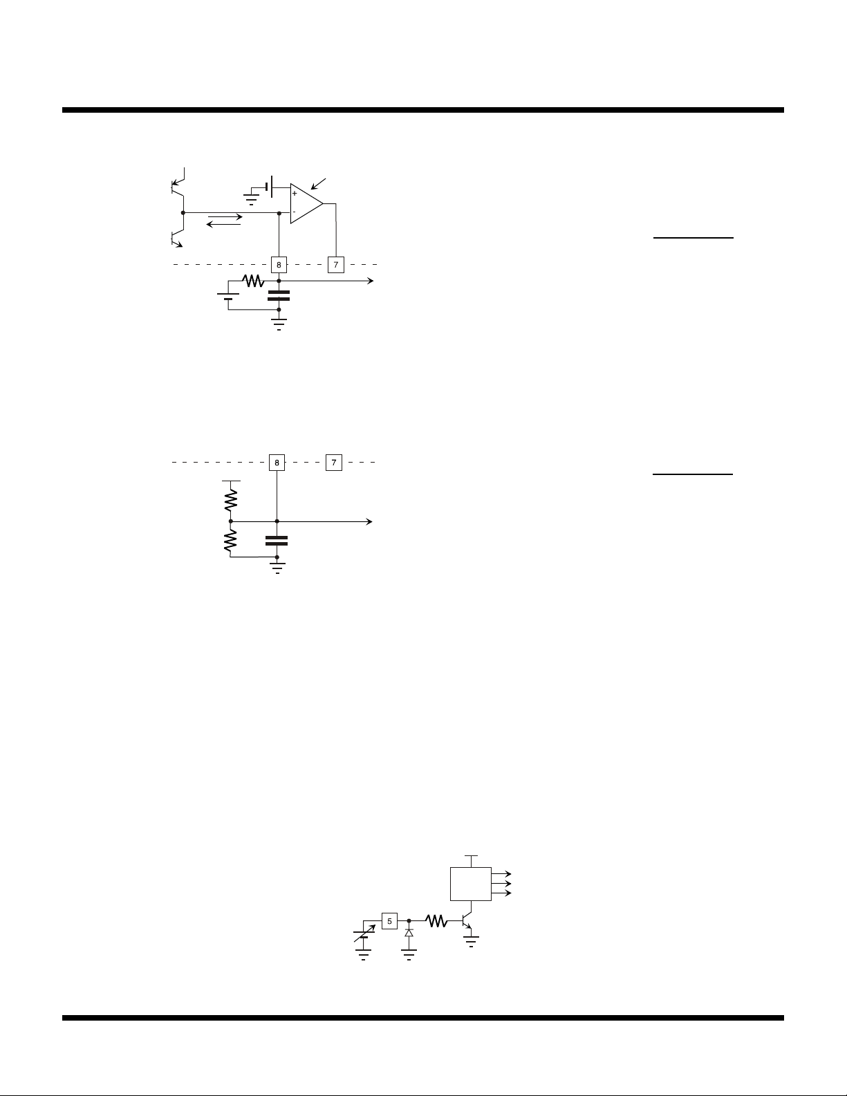
As illustrated in Figure 8, the demodulated output current at Pin 8 is converted to the voltage by an external resistor R1
without using the internal OP AMP.
Figure 9 shows an example of a simple circuit that divides the supply voltage into halves using resistors. Since both circuits
have a high output impedance, an external buffer amplifier should be connected.
January 2000 TOKO, Inc. Page 17
Page 18
TK14584
CIRCUIT DESCRIPTION (CONT.)
V
ref
I to V convertor
Demodulated Output Voltage V
= VB ± R1 x io
OUT
io
Demodulated
Output Current
Fc =
1
2 π C1(1/gm)
1/gm is approximately 50 kΩ which is the output
Demodulated Bandwidth
VB
Demodulated
R1
C1
Output Voltage
V
OUT
resistance of the multiplier.
Pin 7 is disconnected.
FIGURE 8 - EXAMPLE OF USING EXTERNAL REFERENCE SOURCE
Demodulated Output Voltage V
V
CC
R1
R2
C1
Demodulated
Output Voltage
V
OUT
Demodulated Bandwidth
1/gm is approximately 50 kΩ which is the output
= VCC/2 ± R1 x io
OUT
Fc =
1
2 π C1(1/gm)
resistance of the multiplier.
R1 = R2
Pin 7 is disconnected.
FIGURE 9 - EXAMPLE OF DIVIDING SUPPLY VOLTAGE INTO HALVES BY THE RESISTORS
Power Save Function:
Pin 5 is the control terminal for the battery save function. The ON/OFF operation of the whole IC can be switched by
controlling the DC voltage at this terminal. Figure 10 shows the internal equivalent circuit of Pin 5.
Because it switches the bias circuit of the entire IC by using the transistor in standby mode, it reduces the supply current
to near zero. As the input terminal is connected with an electrostatic discharge protection diode at GND side only, it is
possible to control the voltage above the supply voltage. It is possible to go into standby mode by disconnecting Pin 5,
but it is not recommended because Pin 5 is a high impedance and may malfunction by an external disturbance.
When Pin 5 is disconnected, a suitable capacitor should be connected between Pin 5 and GND.
V
CC
BIAS
50 K
Vs
FIGURE 10
Page 18 January 2000 TOKO, Inc.
Page 19
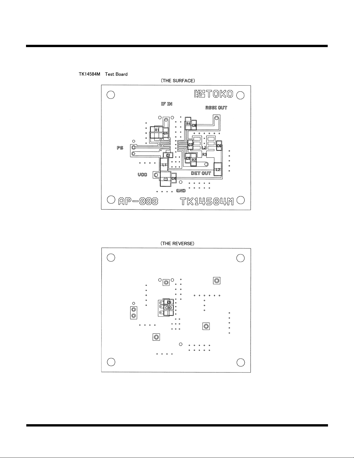
TEST BOARD
TK14584
C1 = C2 = C4 = C6 = C8 = C9 = C10 = 0.01 µF
C3 = 4.7 µF, C5 = 1000 pF, C7 = 1 pF
R1 = 51 Ω, R2 = 51 kΩ, R3 = 3.3 kΩ, R4 = 12 kΩ, R5 = 3 kΩ
L1 = L2 = 10 µH
L3 = 836BH-0268 (TOKO)
January 2000 TOKO, Inc. Page 19
Page 20
TK14584
(
)
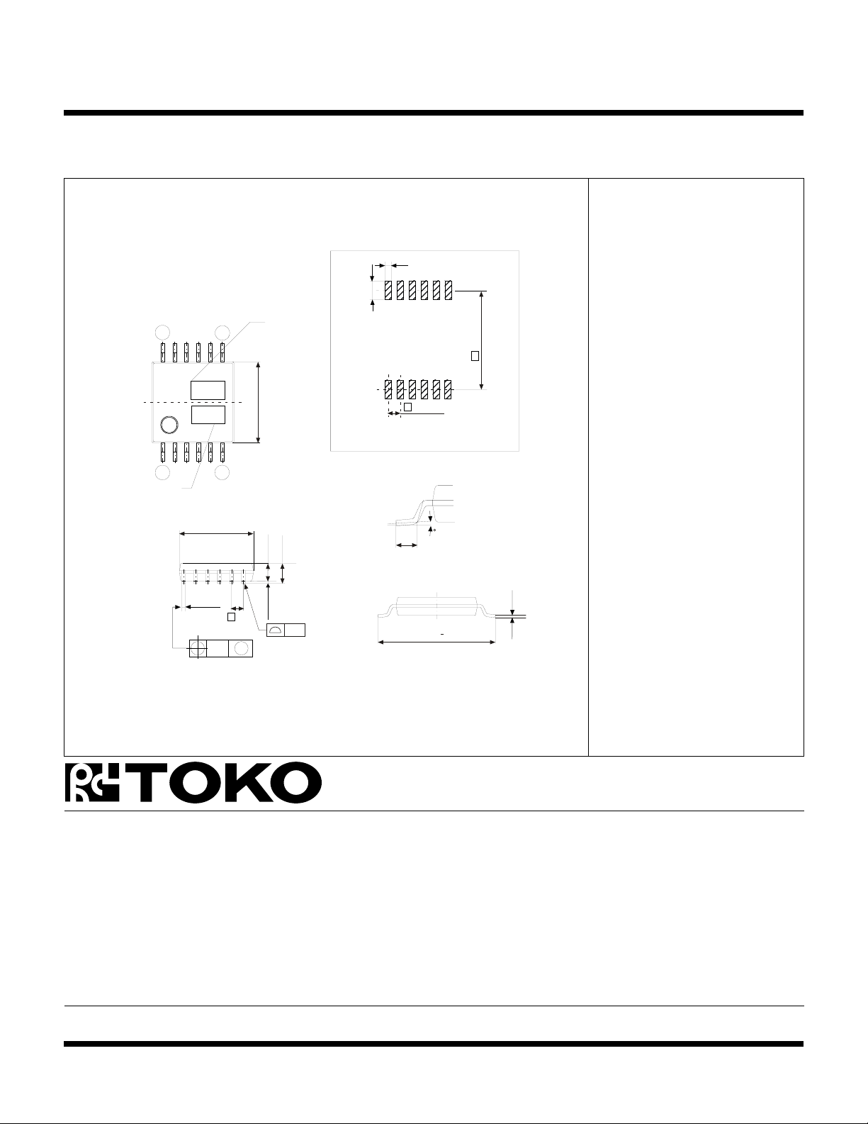
PACKAGE OUTLINE
SSOP-12
12
1
Lot. No.
AAA
YYY
+0.15
-0.05
0.3
5.0
0.10
Marking Information
TK14584M 584
0.4
1.2
7
6
Marking
5.4
e1
4.4
1.4
1.7 max
0 ~ 0.2
e
0.8
M
0.1
e
0.8
Recommended Mount Pad
0 ~ 10
0.5
+
0.3
6.0
+0.15
-0.05
0.15
Dimensions are shown in millimeters
Tolerance: x.x = ± 0.2 mm
unless otherwise specified
Toko America, Inc. Headquarters
1250 Feehanville Drive, Mount Prospect, Illinois 60056
Tel: (847) 297-0070 Fax: (847) 699-7864
TOKO AMERICA REGIONAL OFFICES
Midwest Regional Office
Toko America, Inc.
1250 Feehanville Drive
Mount Prospect, IL 60056
Tel: (847) 297-0070
Fax: (847) 699-7864
Western Regional Office
Toko America, Inc.
2480 North First Street , Suite 260
San Jose, CA 95131
Tel: (408) 432-8281
Fax: (408) 943-9790
Eastern Regional Office
Toko America, Inc.
107 Mill Plain Road
Danbury, CT 06811
Tel: (203) 748-6871
Fax: (203) 797-1223
Semiconductor Technical Support
Toko Design Center
4755 Forge Road
Colorado Springs, CO 80907
Tel: (719) 528-2200
Fax: (719) 528-2375
Visit our Internet site at http://www.tokoam.com
The information furnished by TOKO, Inc. is believed to be accurate and reliable. However, TOKO reserves the right to make changes or improvements in the design, specification or manufacture of its
products without further notice. TOKO does not assume any liability arising from the application or use of any product or circuit described herein, nor for any infringements of patents or other rights of
third parties which may result from the use of its products. No license is granted by implication or otherwise under any patent or patent rights of TOKO, Inc.
Page 20 January 2000 TOKO, Inc.
All Rights Reserved
IC-119-TK119xx
0798O0.0K
Printed in the USA© 1999 Toko, Inc.
 Loading...