

Page 1
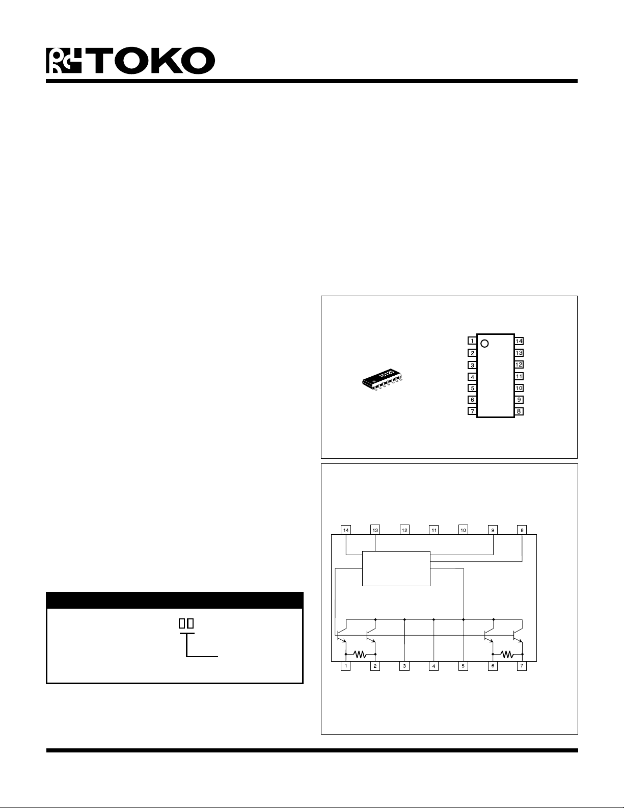
TK15125
Dual Supply Grand Earthing System Audio Signal Mute IC
FEATURES
■ Wide Voltage Range (±2.5 to ±5.5 V)
■ High Volume Attenuation (typ. -89dB)
■ Very Low Signal Distortion (typ. 0.0025%)
■ High Maximum Input Voltage (max. 5.2 V
P-P
)
■ Very Low Standby Current (typ. 0.6 mA)
■ Minimal External Component Circuitry
DESCRIPTION
The TK15125M is a dual power supply Mute IC of the
Grand Earthing System that was developed as a low
frequency signal attenuator for audio products.
The mute function includes two channels which operate
simultaneously by one control key.
The optional time for the Attack/Release action can be set
up by an external timing control capacitor.
APPLICATIONS
■ Audio Systems
■ Television
■ VTR
■ MD
■ CD
TK15125
OUT/IN 1
IN/OUT 1
GND 1
GND 2
GND 3
IN/OUT 2
OUT/IN 2
V
DD
MUTE-C
NC
NC
NC
CONTROL
V
SS
The TK15125M is available in a SOP-14 Surface Mount
Package.
ORDERING INFORMATION
TK15125M
Tape/Reel Code
TAPE/REEL CODE
TL: Tape Left
DD
MUTE-C
V
CONTROL DRIVER TIMING
OUT/IN 1
IN/OUT 1
BLOCK DIAGRAM
NC
GND 2
NC
GND 3
NC
GND 1
CONTROL
IN/OUT 2
SS
V
OUT/IN 2
Control
Lo: Mute off
Hi: Mute on
July 1999 TOKO, Inc. Page 1
Page 2

TK15125
ABSOLUTE MAXIMUM RATINGS
Supply Voltage ......................................................... ±6 V
Power Dissipation (Note 3) ................................ 350 mW
Input Frequency ..................................................100 kHz
Storage Temperature Range ................... -55 to +150 °C
Operating Temperature Range ...................-20 to +60 °C
Signal Input Voltage ......................................... VSS to V
TK15121M ELECTRICAL CHARACTERISTICS
Test conditions: V
LOBMYSRETEMARAPSNOITIDNOCTSETNIMPYTXAMSTINU
V
DD
V
SS
I
)FFO(DD
I
)NO(DD
TTAnoitaunettAR
IC
NO
IC
FFO
VWS
FFO
= ±5 V, T
CC
egatloV
= 25 °C, f = 1 kHz, V
A
egatloVgnitarepO
ffOetuM,tnerruCgnitarepO 6.09.0Am
nOetuM,tnerruCgnitarepO 0.210.71Am
NI
tnerruCegrahCnOetuM0.80.210.81Aµ
tnerruCegrahcsiDffOetuM)2etoN(8.10.30.5Aµ
ffOetuM,WSlortnoCetuM
SIN
= 5 V
unless otherwise specified.
P-P
003= Ω )1etoN(58-98-Bd
DD
5.20.55.5V
5.2-0.5-5.5-V
V
SS
V
4.0+V
SS
VWS
NO
IWS
NO
V
TASO
egatloV
tnerruC
1DHT
2DHTNOretliFA-SIJ7000.00300.0%
noitrotsiD
nOetuM,WSlortnoCetuM
V
nOetuM,WSlortnoCetuM
egatloVCDtuptuOnOetuM 4.27.3Vm
cinomraHlatoTffOetuM
4.2+V
SS
DD
6152Aµ
5200.00700.0%
V
AVGniaGegatloVzHk02~=Bd5.0-05.0+Bd
V
)XAM(NI
RMecnatsiseRnoitaunettArennI861042213
Note 1: If an RIN other than 300 Ω is used, the volume attenuation and attack/release times change.
Note 2: In the standard application a capacitor is connected between Pin 13 and VSS. Attack is the term used to describe the action of changing the
unit from ‘mute off’ to ’mute on’. Release is the term used to describe the action of changing the unit from ‘mute on’ to ‘mute off’. The standard
timing control capacitance is 0.047 µF.
Note 3: Power dissipation is 350 mW when mounted as recommended. Derate at 2.8 mW/°C for operation above 25°C.
egatloVtupnImumixaM%10.0<DHT2.5V
P-P
Ω
Page 2 July 1999 TOKO, Inc.
Page 3
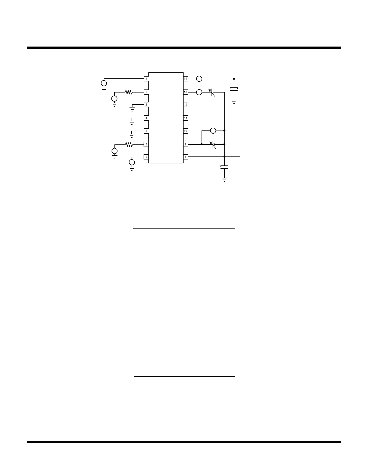
TEST CIRCUIT AND TESTING METHODS
V
+
+5 V
22 µF
DD
VM
300 Ω
SG
A1
A2
NC
TK15125
NC
NC
V1
V
SS
-5 V
22 µF
+
SG
TESTING METHODS
1) POWER SUPPLY CURRENT
GND
300 Ω
VM
· ‘MUTE OFF’ Mode
Measure current ‘A1’ while control, Pin 9, is ‘Lo’ (or open).
· ‘MUTE ON’ Mode
Measure current ‘A1’ while control, Pin 9, is ‘Hi’.
2) ATTENUATION VOLUME
· Attenuation is calculated by the following equation while control, Pin 9, is ‘Hi’:
Pin 1(Pin 7) output AC voltage
ATT = 20Log
(
Pin 2(Pin 6) input AC voltage
)
3) CAPACITOR PIN CHARGING AND DISCHARGING CURRENT
· Charging Current
Measure outflow current ‘A2’ while control, Pin 9, is ‘Hi’ and the voltage at Pin 13 is VSS + 0.75 V.
· Discharging Current
Measure inflow current ‘A2’ while control, Pin 9, is ‘Lo (or open)’ and the voltage at Pin 13 is VSS + 0.75 V.
4) CONTROL SWITCH VOLTAGE
· ‘MUTE OFF’ Mode
Gradually elevate Pin 9 voltage above VSS. When the Attack action (Mute On) is implemented at Pin 1 (Pin 7),
measure the voltage ‘V1’.
· ‘MUTE ON’ Mode
Gradually lower Pin 9 voltage below VDD. When the Release action (Mute Off) is implemented at Pin 1 (Pin 7),
measure the voltage ‘V1’.
5) ‘MUTE ON’ OUTPUT DC VOLTAGE
· Measure output voltage at Pin 1 (Pin 7) while control, Pin 9, is ‘Hi’ and there is no input.
6) TOTAL HARMONIC DISTORTION
· Measure the distortion of the Pin 1 (Pin 7) output while control, Pin 9, is ‘Lo’ (or open).
7) SIGNAL VOLTAGE GAIN
· Signal gain is calculated by the following equation while control, Pin 9, is ‘Lo’ (or open).
Pin 1(Pin 7) output AC voltage
GV = 20Log
(
Pin 2(Pin 6) input AC voltage
)
8) INNER ATTENUATION RESISTANCE
· Using a multimeter, measure the resistance between Pin 1 (Pin 7) and Pin 2 (Pin 6) while the power supply is
off.
9) MAXIMUM INPUT SIGNAL VOLTAGE
· While control, Pin 9, is ‘Lo’ (or open), gradually elevate Pin 2 (Pin 6) voltage above 0 V
becomes 0.01% at the output of Pin 1 (Pin 7), measure the AC voltage.
. When the distortion
P-P
July 1999 TOKO, Inc. Page 3
Page 4
TK15125
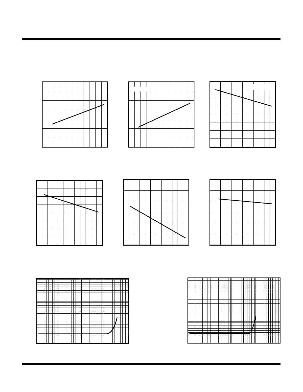
TYPICAL PERFORMANCE CHARACTERISTICS
TA = 25 °C, unless otherwise specified.
SUPPLY CURRENT
vs. SUPPLY VOLTAGE
Mute: off
0 2 3 4 5 6
V
CC
CONTROL THRESHOLD
VOLTAGE vs. TEMPERATURE
(mA)
CC
I
-3
-3.5
(V)
-4
CONT
V
-4.5
0.7
0.6
0.5
0.4
(±V)
SUPPLY CURRENT
vs. SUPPLY VOLTAGE
Mute: on
13
12
(mA)
CC
I
11
10
0 2 3 4 5 6
V
CC
CHARGE CURRENT (Mute Pin)
16
15
14
(µA)
13
12
CURRENT
11
vs. TEMPERATURE
(±V)
SUPPLY CURRENT
14
12
(mA)
10
CC
I
8
6
-40 -20 0 20 40 60 80
4
3
(µA)
2
CURRENT
vs. TEMPERATURE
Mute: on
TA (°C)
DISCHARGE CURRENT (Mute Pin)
vs. TEMPERATURE
-5
-40 -20 0 20 40 60 80
TA (°C)
TOTAL HARMONIC DISTORTION
vs. FREQUENCY
1
0.1
THD (%)
0.01
0.001
0.01 0.1 1 10 100
f (kHz)
10
-40 -20 0 20 40 60 80
TA (°C)
0.1
THD (%)
0.01
0.001
1
0.01 0.1 1 10 100
0
-40 -20 0 20 40 60 80
TA (°C)
TOTAL HARMONIC DISTORTION
vs. OUTPUT VOLTAGE
V
(V
P-P
)
OUT
Page 4 July 1999 TOKO, Inc.
Page 5
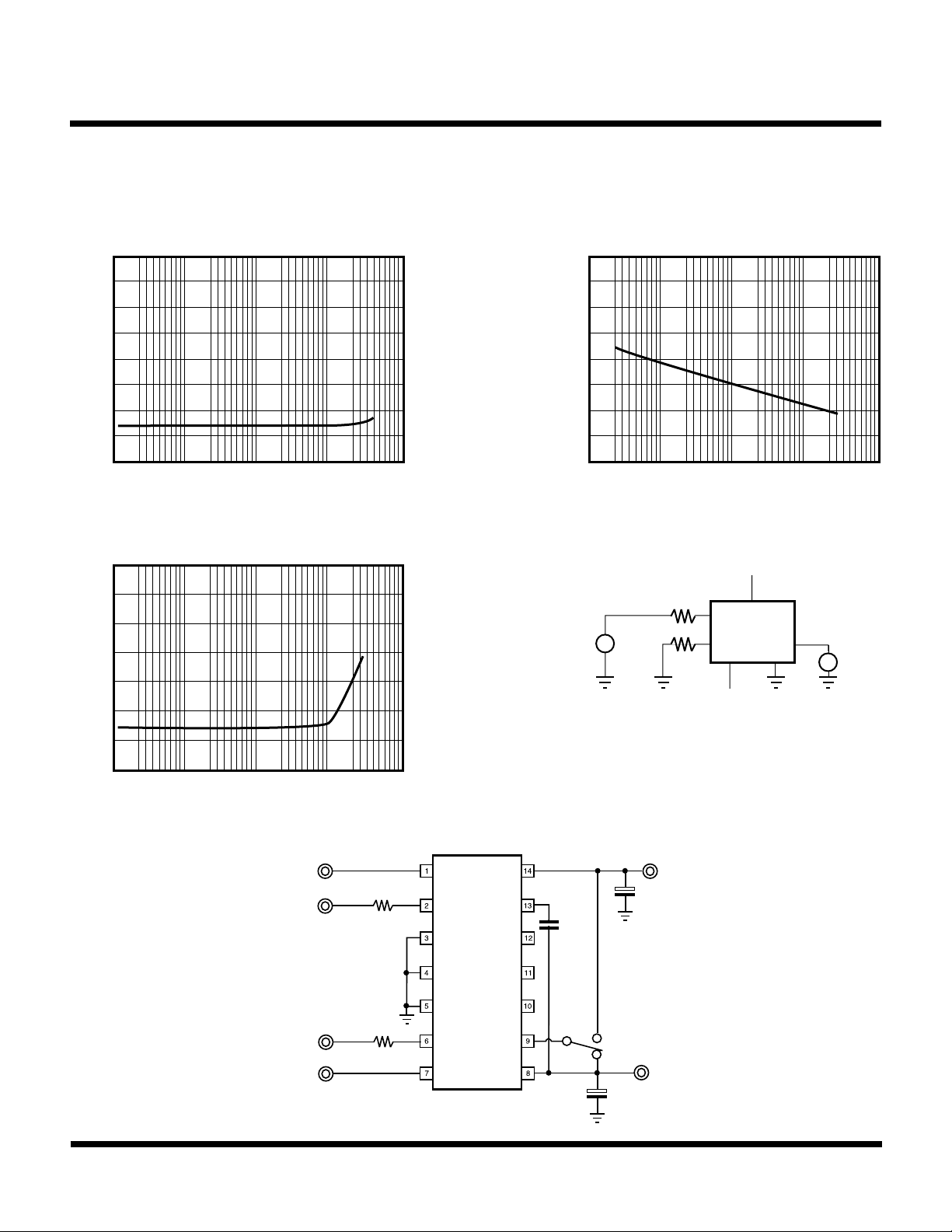
TYPICAL PERFORMANCE CHARACTERISTICS (CONT.)
ATT (dB)
-40
ATTENUATION VOLUME
vs. MUTE RESISTANCE
RESISTANCE (kΩ)
-120
0.01 0.1 1 10 100
-60
-80
-100
CROSS
TALK
(dB)
TA = 25 °C, unless otherwise specified.
ATTENUATION VOLUME
vs. FREQUENCY
-20
-40
-60
ATT (dB)
-80
-100
0.01 0.1 1 10 100
f (kHz)
CROSS TALK
vs. FREQUENCY
-80
-90
-100
~
5 V
P-P
300
300
I/O 1
I/O 2
-5 V
TK15125
+5 V
O/I 1
O/I 2
V
~
-110
0.01 0.1 1 10 100
f (kHz)
July 1999 TOKO, Inc. Page 5
OUT 1
IN 1
IN 2
OUT 2
STANDARD APPLICATION
300
300
on
off
0.047 µF
22 µF
+
Cross Talk Test Circuit
+5 V
+
22 µF
on
off
-5 V
Page 6
TK15125
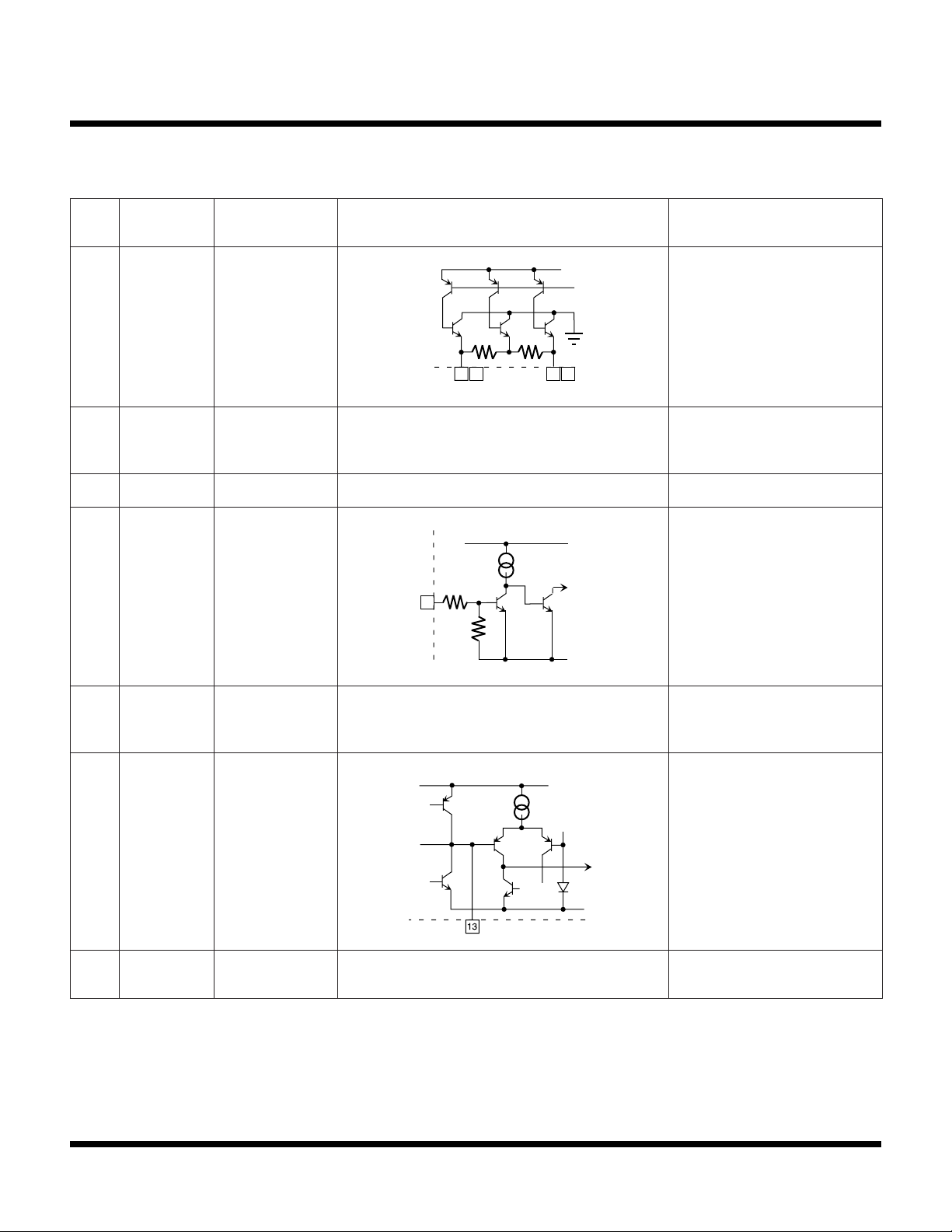
TERMINAL VOLTAGE AND EQUIVALENT CIRCUIT
NIP
.ON
1
2
6
7
3
4
5
8V
LOBMYS
1NI/TUO
1TUO/NI
2TUO/NI
2NI/TUO
1DNG
2DNG
3DNG
SS
CD
EGATLOV
V0/gnitaolF
V0/gnitaolF
V0/gnitaolF
V0/gnitaolF
V0
V0
V0
V5.2-~5.5-V
SS
TIUCRICTNELAVIUQENOITANALPXE
V
DD
120
1267
120
.nipDNG.nipdnuorG
.nip.niPegatloVevitageN
9lortnoCV0.5- etuMehtrofniPlortnoC
V
DD
47 K
9
47 K
V
SS
.2niProftuptuO:1niP
.1niProftupnI:2niP
.7niProftupnI:6niP
.6niProftuptuO:7niP
1etoN
2etoN
.ffo/no
01
11
21
CN
CN
CN
gnitaolF
.niPnoitcennoCoN
gnitaolF
gnitaolF
31C-etuMV2.3/V0.5- roticapaCgnimiTrofniP
V
41V
DD
V5.5~5.2V
.niP.niPegatloVevitisoP
DD
DD
V
SS
.emitesaeleR/kcattArof
Note 1: Even if the input and output became opposite, the action is the same.
Note 2: Connect all GND pins to the Ground.
Note 3: Although all NC pins are not connected internally to the IC, signals should not be externally applied to
these pins.
Note 4: In the standard application a capacitor is connected between Pin 13 and VSS. Attack is the term used to describe
the action of changing the unit from ‘mute on’ to ‘mute off’.
The standard timing control capacitance is 0.047 µF.
3etoN
4etoN
Page 6 July 1999 TOKO, Inc.
Page 7
TK15125
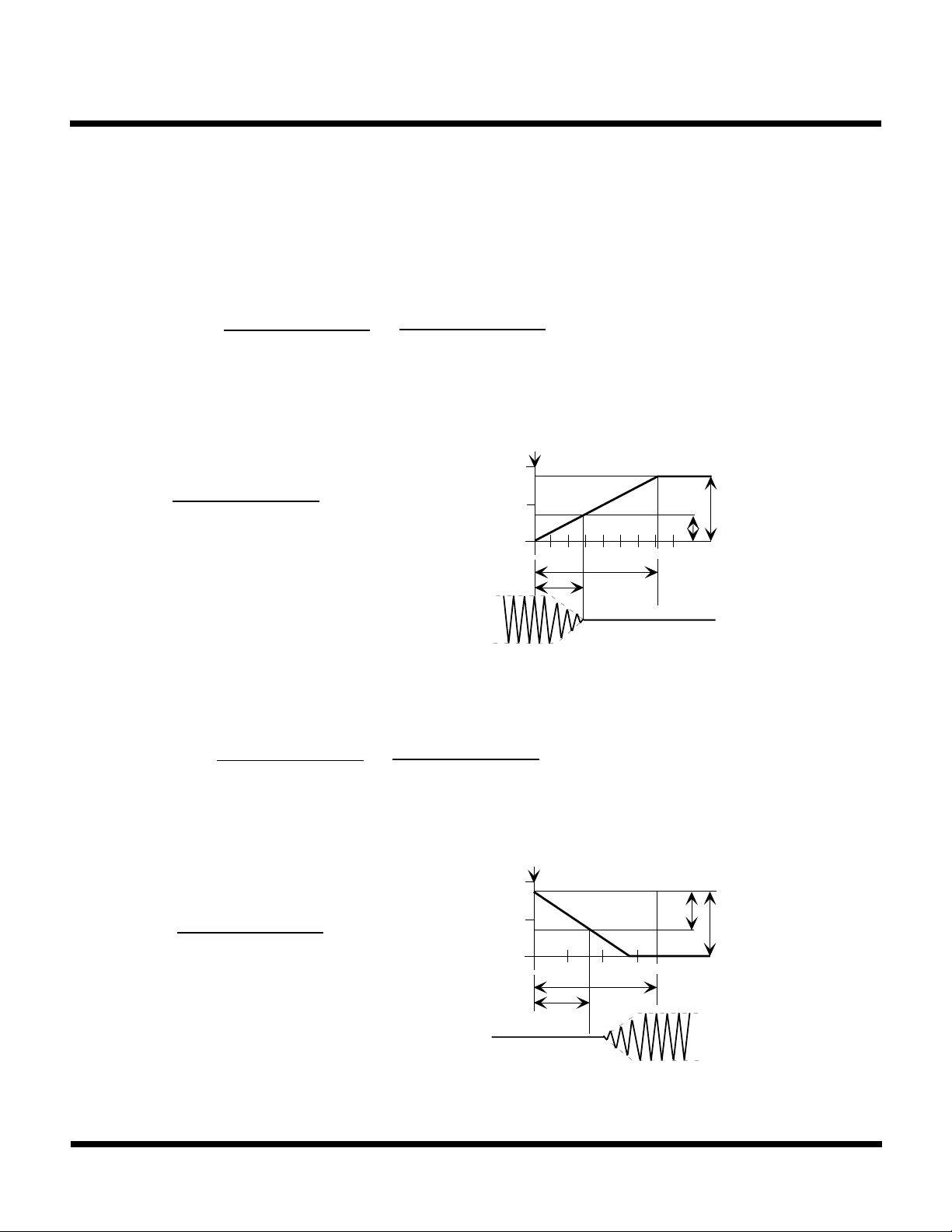
TIMING-CHART AND ACTION TIME AT MUTE
Test conditions: V
The following values are typical characteristics; accordingly they are not guaranteed values.
ATTACK ACTION START (MUTE ON)
When the attack action is started (‘mute on’ is initiated), the capacitor on Pin 13 starts to charge. The voltage at the
capacitor on Pin 13 rises by 1.8 V. The 1.8 V rise time can be calculated by the following equation:
When the capacitor of Pin 13 rises by 1.8 V to -3.2 V as detected by the upper limit circuit, the mute action functions
(VSS + 1.8 V = -3.2 V). In this estimate, when the capacitor on Pin 13 has risen by 0.7 V to 0.8 V, the attenuation is
approximately 90% of the final attenuation achieved. This results in the following calculation and timing chart.
T2 ≈
= 2.9 msec
This time is the attack time.
= ±5 V, Timing Capacitor = 0.047 µF
CC
T1 ≈
Capacitance X 1.8 V
Charge Current
0.047 µF X 0.75 V
12 µA
0.047 µF X 1.8 V
=
12 µA
= 7.1 msec
Control SW_on
-3 V
-4 V
-5 V
Pin 13
1 2 3 4 5 6 7 8 (ms)
T1
T2
Capacitor pin voltage
1.8 V
0.75 V
Input
wave
Output
wave
RELEASE ACTION START (MUTE OFF)
When the release action is started (‘mute off’ is initiated) the capacitor on Pin 13 starts to discharge. The voltage
at the capacitor on Pin 13 falls to VSS + 10 mV. This fall time can be calculated by the following equation:
T3 ≈
Capacitance X 1.8 V
Disharge Current
0.047 µF X 1.8 V
=
3 µA
= 28 msec
In this estimate, when the capacitor on Pin 13 has fallen to VSS + 0.7 V to 0.8 V, the signal is restored to approximately
90% of its value. This results in the following calculation and timing chart:
Control SW_off
-3 V
T4 ≈
0.047 µF X 1.05 V
3 µA
= 16 msec
This time is the release time.
Accordingly, the release action time is 12 msec
-4 V
-5 V
Pin 13
10 20 30 (ms)
T4
T3
1.05 V
1.8 V
Capacitor pin voltage
Output
wave
(T3 - T4 = 28 msec - 16 msec = 12 msec).
July 1999 TOKO, Inc. Page 7
Page 8
TK15125
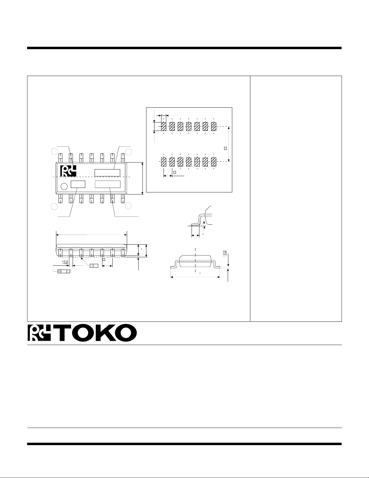
PACKAGE OUTLINE
SOP-14
14
1
0.42
Lot No.
0.12
YYY
M
AAAAA
KOREA
8.65
0.1
e
1.27
MarkToko Mark
8
7
Country of Origin
3.9
0.3
+
1.45
0 ~ 0.25
1.64
1.27
0.76
e
1.27
Recommended Mount Pad
0.5
6.07
Marking Information
TK15125M 15125
5.4
1
e
0 ~10
0.2
+
0.3
Dimensions are shown in millimeters
Tolerance: x.x = ± 0.2 mm (unless otherwise specified)
Toko America, Inc. Headquarters
1250 Feehanville Drive, Mount Prospect, Illinois 60056
Tel: (847) 297-0070 Fax: (847) 699-7864
TOKO AMERICA REGIONAL OFFICES
Midwest Regional Office
Toko America, Inc.
1250 Feehanville Drive
Mount Prospect, IL 60056
Tel: (847) 297-0070
Fax: (847) 699-7864
Western Regional Office
Toko America, Inc.
2480 North First Street , Suite 260
San Jose, CA 95131
Tel: (408) 432-8281
Fax: (408) 943-9790
Eastern Regional Office
Toko America, Inc.
107 Mill Plain Road
Danbury, CT 06811
Tel: (203) 748-6871
Fax: (203) 797-1223
Semiconductor Technical Support
Toko Design Center
4755 Forge Road
Colorado Springs, CO 80907
Tel: (719) 528-2200
Fax: (719) 528-2375
Visit our Internet site at http://www.tokoam.com
The information furnished by TOKO, Inc. is believed to be accurate and reliable. However, TOKO reserves the right to make changes or improvements in the design, specification or manufacture of its
products without further notice. TOKO does not assume any liability arising from the application or use of any product or circuit described herein, nor for any infringements of patents or other rights of
third parties which may result from the use of its products. No license is granted by implication or otherwise under any patent or patent rights of TOKO, Inc.
Page 8 July 1999 TOKO, Inc.
All Rights Reserved
IC-119-TK119xx
0798O0.0K
Printed in the USA© 1999 Toko, Inc.
 Loading...