

Page 1
TK15400
75 Ω VIDEO LINE DRIVER
FEATURES
■ Fixed Gain (6 dB)
■ Internal 75 Ω Drivers
■ Very Small Output Capacitor Using SAG
Function Pin
■ Active High ON/OFF Control
■ Very Low Standby Current (typ. I
≤ 25 µA)
STBY
■ Internal Summing Circuit of Y/C Signal
■ Single +5 V Power Supply Operation
DESCRIPTION
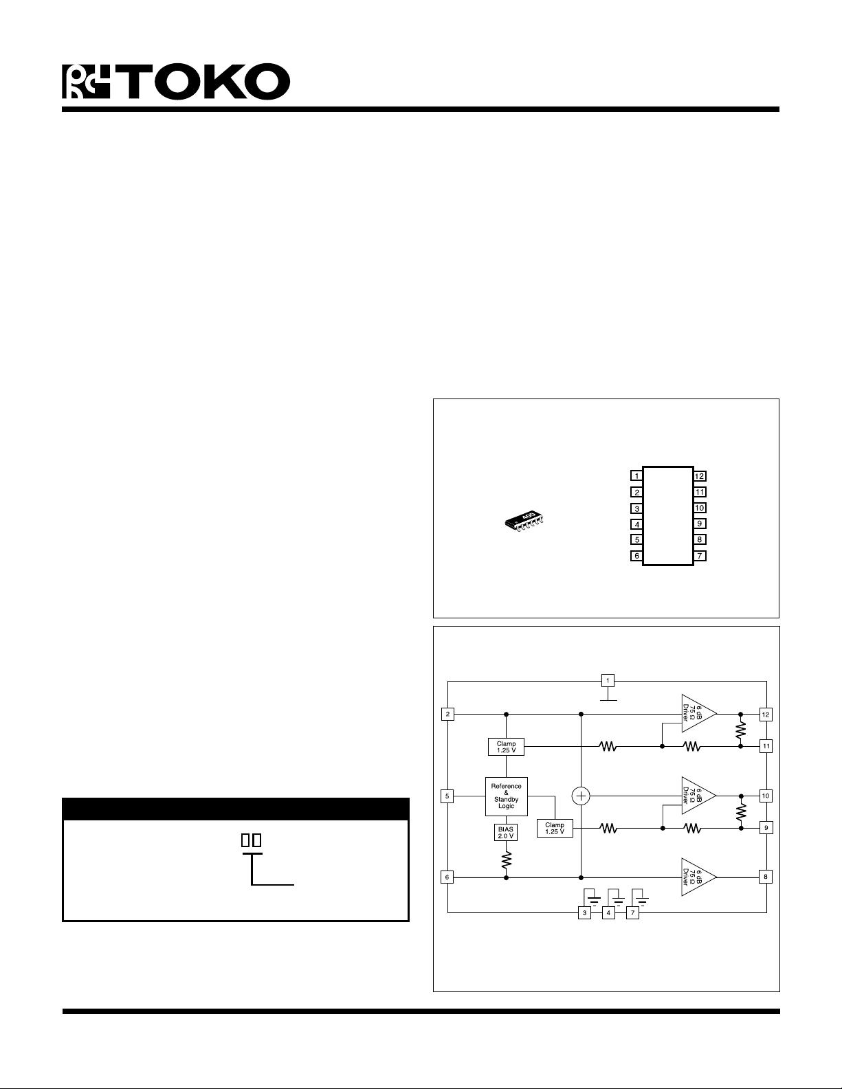
Operating from a single +5 V supply, the TK15400 is a
triple video line driver IC that takes standard Y/C analog
inputs and provides simultaneous Y/C and composite
analog outputs for driving 75 Ω lines. Internal summing of
the Y and C inputs is performed to produce the composite
video output. The luminance (Y) input is clamped at
1.25 V and amplified 6 dB to produce 2 V
a series 75 Ω resistor and 75 Ω cable load. The internal
1.5 k SAG function resistor provides gain compensation
for low frequency signals. The chromanance (C) input is
biased at 2.0 V and amplified 6 dB to produce 1.3 V
(typical) into a series 75 Ω resistor and 75 Ω cable load.
During standby (Pin 5 grounded), the TK15400 consumes
only 113 µW of power. Nominal power dissipation (no
input) is typically 168 mW.
The TK15400M is available in the SSOP-12 Surface
Mount Package.
(typical) into
P-P
P-P
APPLICATIONS
■ Video Equipment
■ Digital Cameras
■ CCD Cameras
■ TV Monitors
■ Video Tape Recorders
■ LCD Projectors
TK15400
BLOCK DIAGRAM
V
CC
Y-INPUT
GND
GND
STANDBY
C-INPUT
V
CC
5 k 5 k
Y-OUTPUT
Y-SAG
CVBS-OUTPUT
CVBS-SAG
C-OUTPUT
GND
1.5 k
ORDERING INFORMATION
TK15400M
Tape/Reel Code
TAPE/REEL CODE
TL: Tape Left
5 k 5 k
100 k
1.5 k
January 2000 TOKO, Inc. Page 1
Page 2

TK15400
ABSOLUTE MAXIMUM RATINGS
Supply Voltage ........................................................... 6 V
Operating Voltage ......................................... 4.5 to 5.5 V
Storage Temperature Range ................... -55 to +150 °C
Operating Temperature Range ...................-25 to +75 °C
Power Dissipation (Note 1) ................................ 350 mW
TK15400M ELECTRICAL CHARACTERISTICS
Test conditions: V
LOBMYSRETEMARAPSNOITIDNOCTSETNIMPYTXAMSTINU
I
CC
I
YBTS
I
SO
V
LHT
V
HLT
V
PMC
V
SAIB
AVGniaGegatloVC
GDniaGlaitnereffiDtupnievawesacriatS0.3-5.1-0.3+%
= 5.0 V, VIN = 1.0 V
CC
tnerruCylppuStupnioN5.330.54Am
)woL
)hgiH
egatloVpmalClanimrettupnilangisY2niP50.152.154.1V
egatloVsaiBlanimrettupnilangisC6niP07.100.203.2V
, RL = 150 Ω, TA = 25 °C unless otherwise specified.
P-P
tnerruCylppuSybdnatSdednuorG5niP5.220.05Aµ
tnerruClanimreTybdnatSedomybdnatS5niP5.220.05Aµ
othgiH(egatloVdlohserhT
edom
otwoL(egatloVdlohserhT
edom
C-
NI
TUOf,ni
ybdnatSotgnitarepO5niP
gnitarepOotybdnatS5niP
DNG1.03.0V
8.10.2V
CC
ZHM1=5.50.65.6Bd
V
PDesahPlaitnereffiDtupnievawesacriatS0.3-2.0-0.3+ged
rfesnopseRycneuqerFf
1TC1klaTssorCY
2TC2klaTssorCC
Note 1: Power dissipation is 350 mW in free air. Derate at 2.8 mW/°C for operation above 25°C.
ni
C-
NI
TUO
Y-
NI
TUO
zHM5/zHM1=0.0Bd
04-Bd
04-Bd
Page 2 January 2000 TOKO, Inc.
Page 3
Y-INPUT
TP1
C-INPUT
TP2
4.7 µF
75 Ω
Standby
4.7 µF
75 Ω
TEST CIRCUIT
V
CC
VCC = 5.0 V
33 µF
+
33 µF
+
33 µF
+
33 µF
+
33 µF
+
33 µF
TP7
TP5
TP3
Y-OUTPUT
V
OUT
V
OUT
C-OUTPUT
V
OUT =
= 2.0 V
75 Ω
CVBS
= 2.0 V
75
Ω
1.3 V
75 Ω
TK15400
P-P
TP8
75 Ω
P-P
TP6
75 Ω
P-P
TP4
75 Ω
GND
MEASUREMENT METHOD
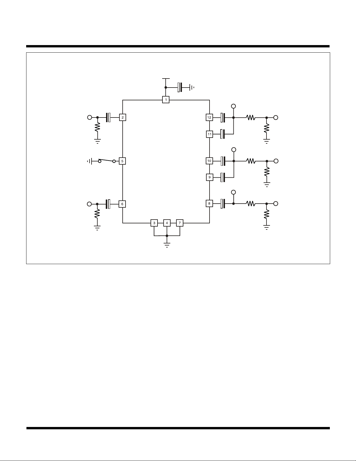
1. Supply Current (ICC)
The Pin 1 current is measured with no input signal and the Standby Pin (Pin 5) open.
2. Standby Supply Current (I
STBY
)
The Pin 1 current is measured when the Standby Pin (Pin 5) is connected to ground.
3. Standby Terminal Current (IOS)
The Pin 5 current is measured when Pin 5 is connected to ground.
4. Threshold Voltage (High to Low) (V
THL
)
The Pin 5 voltage is measured at the point which changes the device from operating mode into standby mode.
5. Threshold Voltage (Low to High) (V
TLH
)
The Pin 5 voltage is measured at the point which changes the device from standby mode into operating mode.
6. Clamp Voltage (V
CMP
)
The DC voltage at Pin 2 is measured with no input signal.
January 2000 TOKO, Inc. Page 3
Page 4

TK15400
MEASUREMENT METHOD (CONT.)
7. Bias Voltage (V
BIAS
)
The DC voltage at Pin 6 is measured with no input signal.
8. Voltage Gain (GVA)
The voltage gain equation is as follows:
GVA = 20 log10 V2/V1
Where V1 is the input voltage at TP1 and V2 is the measured voltage at TP5 (TP7). Furthermore, V1 is the input voltage
at TP2 and V2 is the measured voltage at TP3 (TP5).
9. Differential Gain (DG)
The differential gain is measured at TP5 (TP7) when a staircase waveform of 10 steps is applied to TP1.
10. Differential Phase (DP)
The differential phase is measured at TP5 (TP7) when a staircase waveform of 10 steps is applied to TP1.
11. Frequency Response (fr)
The frequency response equation is as follows:
fr = 20 log10 V2/V1
Where V1 is the measured TP7 voltage when the TP1 input frequency is set to 1 MHz and V2 is the measured TP7 voltage
when the TP1 input frequency is set to 5 MHz. Furthermore, V1 is the measured TP3 (TP5) voltage when the TP2 input
frequency is set to 1 MHz and V2 is the measured TP3 (TP5) voltage when the TP2 input frequency is set to 5 MHz.
12. Cross Talk 1 (CT1)
The cross talk equation is as follows:
CT1 = 20 log10 V1/V2
Where V1 is measured at TP3 when a 1 MHz 1 V
MHz 1 V
input signal is applied to TP2.
P-P
input signal is applied to TP1 and V2 is measured at TP3 when a 1
P-P
13. Cross Talk 2 (CT2)
The cross talk equation is as follows:
CT2 = 20 log10 V1/V2
Where V1 is measured at TP7 when a 1 MHz 1 V
MHz 1 V
input signal is applied to TP1.
P-P
input signal is applied to TP2 and V2 is measured at TP7 when a 1
P-P
Page 4 January 2000 TOKO, Inc.
Page 5
TYPICAL PERFORMANCE CHARACTERISTICS
I
STBY
(µA)
10
40
STANDBY SUPPLY CURRENT
VS.
SUPPLY VOLTAGE
V
CC
(V)
0
4.0 4.5 5.0 5.5 6.0
30
50
TA = 25 °C,
Pin 5 = GND
20
TK15400
SUPPLY CURRENT
VS.
TEMPERATURE
40
VCC = 5.0 V,
No Input
35
(mA)
30
CC
I
25
20
-50 0 50 100
TA (°C)
STANDBY SUPPLY CURRENT
TEMPERATURE
50
VCC = 5.0 V,
40
30
(µA)
Pin 5 = GND
VS.
SUPPLY CURRENT
VS.
SUPPLY VOLTAGE
40
TA = 25 °C,
No Input
35
(mA)
30
CC
I
25
20
4.0 4.5 5.0 5.5 6.0
V
(V)
CC
20
STBY
I
10
0
-50 0 50 100
TA (°C)
VOLTAGE GAIN
8.0
7.0
TEMPERATURE
6.0
GVA (dB)
5.0
4.0
-50 0 50 100
TA (°C)
VS.
VCC = 5.0 V,
fin = 1 MHz,
VIN = 1 V
P-P
VS.
TA = 25 °C,
fin = 1 MHz,
VIN = 1 V
8.0
7.0
VOLTAGE GAIN
SUPPLY VOLTAGE
6.0
GVA (mA)
5.0
4.0
4.0 4.5 5.0 5.5 6.0
V
(V)
CC
P-P
January 2000 TOKO, Inc. Page 5
Page 6
TK15400
TYPICAL PERFORMANCE CHARACTERISTICS (CONT.)
FREQUENCY RESPONSE
TEMPERATURE
1.0
fin = 1/5 MHz,
VIN = 1 V
P-P
0.5
0.0
fc (dB)
-0.5
-1.0
-50 0 50 100
TA (°C)
CLAMP VOLTAGE
VS.
TEMPERATURE
1.5
VCC = 5.0 V,
1.4
1.3
(V)
Pin 2 Voltage
VS.
FREQUENCY RESPONSE
SUPPLY VOLTAGE
1.0
fin = 1/5 MHz,
VIN = 1 V
0.5
0.0
fc (dB)
-0.5
-1.0
4.0 4.5 5.0 5.5 6.0
V
(V)
CC
CLAMP VOLTAGE
SUPPLY VOLTAGE
VS.
1.5
TA = 25 °C,
1.4
1.3
(V)
Pin 2 Voltage
VS.
P-P
CMP
1.2
V
1.1
1.0
-50 0 50 100
TA (°C)
BIAS VOLTAGE
TEMPERATURE
VS.
2.4
VCC = 5.0 V,
Pin 6 Voltage
2.2
(V)
2.0
BIAS
V
1.8
1.6
-50 0 50 100
TA (°C)
CMP
1.2
V
1.1
1.0
4.0 4.5 5.0 5.5 6.0
V
(V)
CC
BIAS VOLTAGE
SUPPLY VOLTAGE
VS.
2.4
TA = 25 °C
Pin 6 Voltage
2.2
(V)
2.0
BIAS
V
1.8
1.6
4.0 4.5 5.0 5.5 6.0
V
(V)
CC
Page 6 January 2000 TOKO, Inc.
Page 7
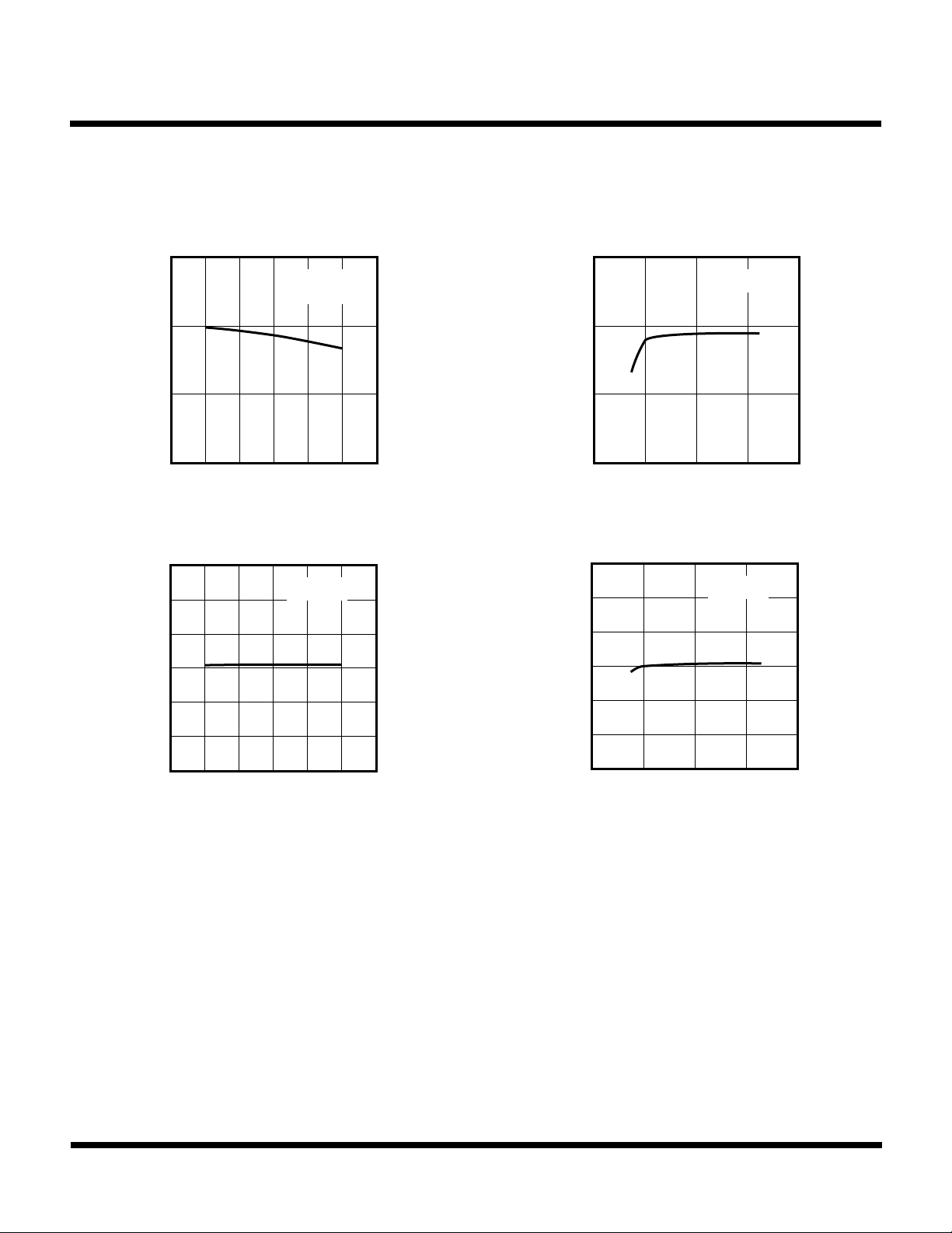
TYPICAL PERFORMANCE CHARACTERISTICS (CONT.)
DG
(%)
TK15400
DIFFERENTIAL GAIN
VS.
TEMPERATURE
10
VCC = 5.0 V,
VIN = 1 V
P-P
0
-10
-20
-50 0 50 100
TA (°C)
DIFFERENTIAL PHASE
TEMPERATURE
6
VCC = 5.0 V,
VIN = 1 V
4
P-P
2
0
DP (deg)
-2
VS.
DIFFERENTIAL GAIN
SUPPLY VOLTAGE
10
TA = 25 °C
VIN = 1 V
0
DG (%)
-10
-20
4.0 4.5 5.0 5.5 6.0
V
(V)
CC
DIFFERENTIAL PHASE
SUPPLY VOLTAGE
6
TA = 25 °C,
4
VIN = 1 V
2
0
DP (deg)
-2
VS.
P-P
VS.
P-P
-4
-6
-50 0 50 100
TA (°C)
-4
-6
4.0 4.5 5.0 5.5 6.0
V
(V)
CC
January 2000 TOKO, Inc. Page 7
Page 8
TK15400
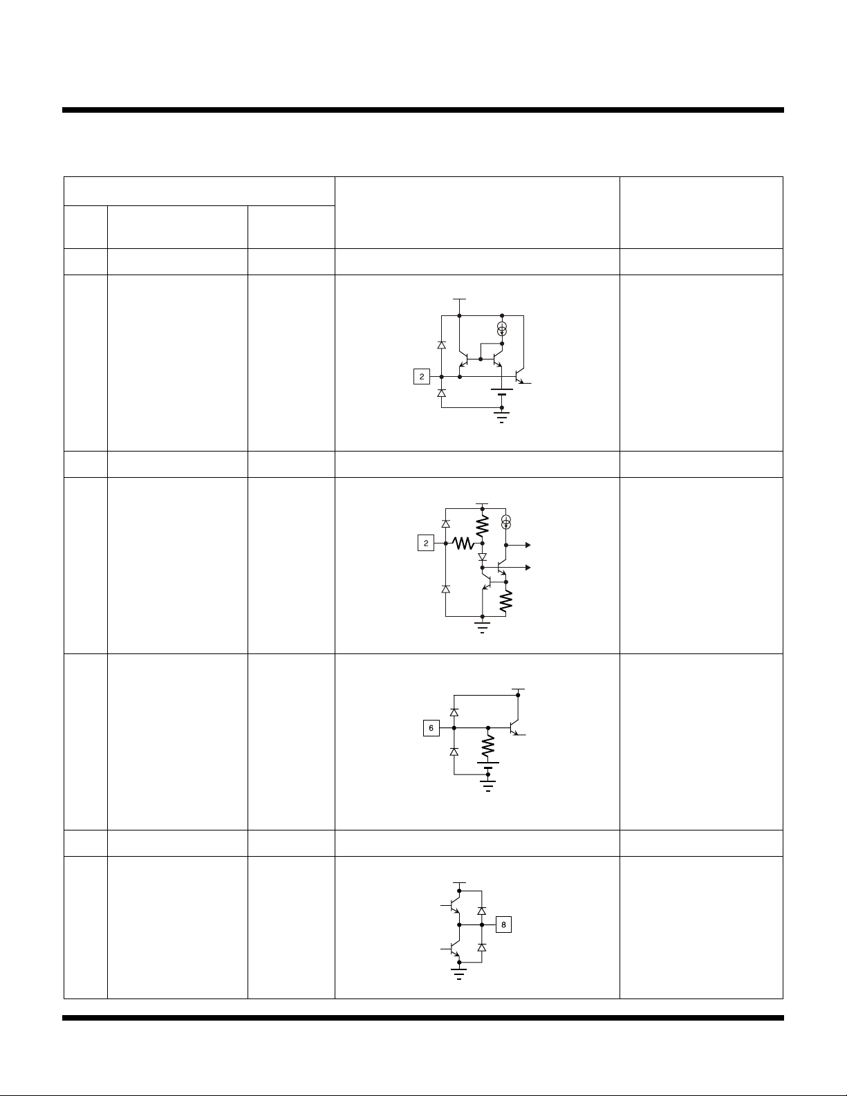
PIN FUNCTION DESCRIPTION
LANIMRET
NIP
.ON
LOBMYSEGATLOV
TIUCRICTNELAVIUQELANRETNINOITPIRCSED
1V
CC
2TUPNI-YV52.1 langisYehtsi2niP
V
CC
V
CC
1.25 V
4,3DNGDNGlanimretDNG
5YBDNATSV4.1 ybdnatsehtsi5niP
200 k
5 k
V
CC
lanimretylppusrewoP
.lanimrettupni
sexiftiucricpmalcehT
suonorhcnyseht
.V52.1otegatlov
.lanimretcigol
ehtnisiecivedehT
5niPnehwetatsevitca
levelhgihotpudellupsi
.neporo
ehtnisiecivedehT
niPnehwetatsybdnats
wolotnwoddellupsi5
.level
6TUPNI-CV0.2 langisCehtsi6niP
V
CC
.lanimrettupni
ehtsexiftiucricsaibehT
ehtybV0.2otlangisC
100 k
2.0 V
k001 Ω .rotsisersaib
7DNGDNGlanimretDNG
8TUPTUO-CV0.2 langisCehtsi8niP
V
CC
.lanimrettuptuo
otelbaliavasi8niP
57aevird Ω 57+ Ω
.daol
Page 8 January 2000 TOKO, Inc.
Page 9
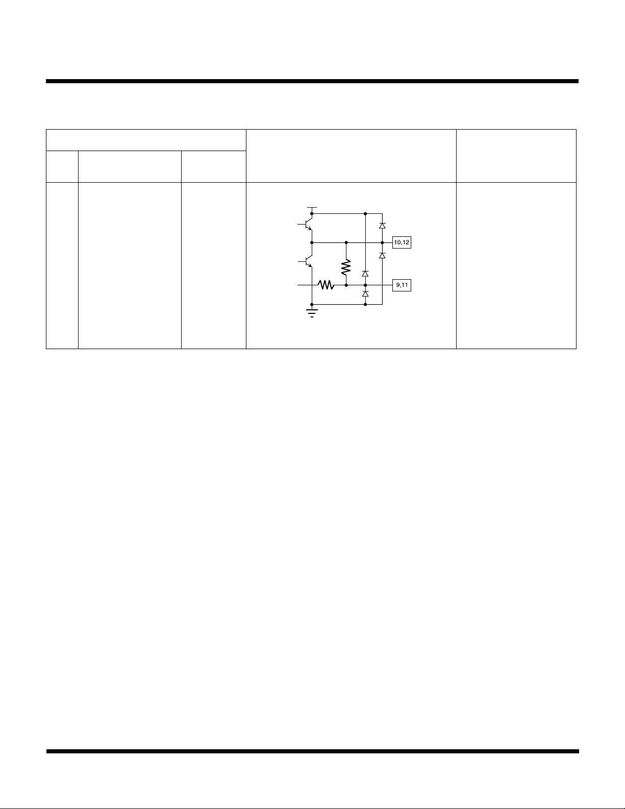
PIN FUNCTION DESCRIPTION
LANIMRET
NIP
.ON
LOBMYSEGATLOV
TK15400
TIUCRICTNELAVIUQELANRETNINOITPIRCSED
9
01
11
21
GAS-SBVC
TUPTUO-SBVC
GAS-Y
TUPTUO-Y
V52.1
V
V52.1
CC
V52.1
V52.1
.lanimretGAS
ehtera01niPdna9niP
tuptuolangisSBVC
-SBVCehtdnalanimret
Yehtera21dna11niP
lanimrettuptuolangis
1.5 k
GAS-Yehtdna
.lanimret
5 k
erasnipesehT
57evirdotelbaliava Ω
57+ Ω .sdaol
January 2000 TOKO, Inc. Page 9
Page 10

TK15400
NOTES
Page 10 January 2000 TOKO, Inc.
Page 11

NOTES
TK15400
January 2000 TOKO, Inc. Page 11
Page 12
TK15400
(
)
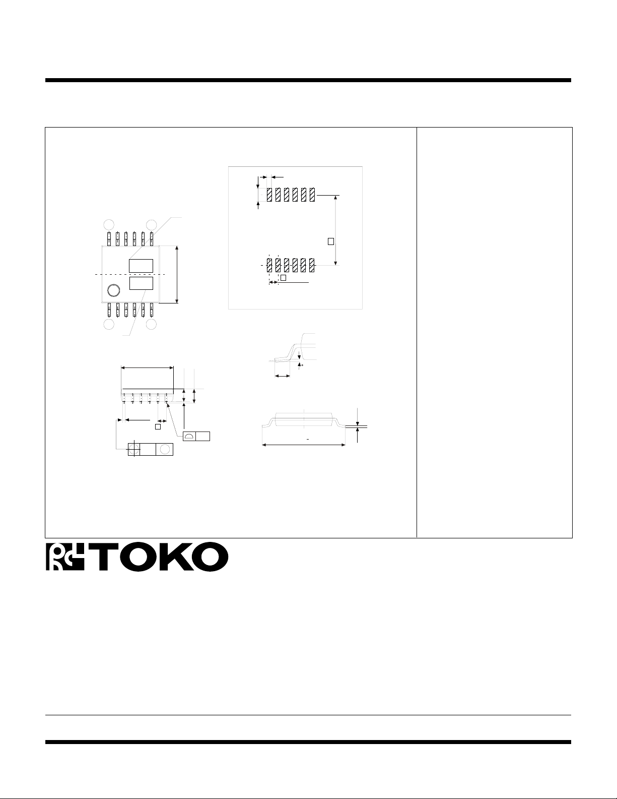
PACKAGE OUTLINE
SSOP-12
12
1
Lot. No.
AAA
YYY
+0.15
-0.05
0.3
5.0
0.10
Marking Information
0.4
1.2
7
6
Marking
5.4
e1
4.4
1.4
1.7 max
0 ~ 0.2
e
0.8
M
0.1
e
0.8
Recommended Mount Pad
0 ~ 10
0.5
+
0.3
6.0
+0.15
-0.05
0.15
Marking
TK15400 400
Dimensions are shown in millimeters
Tolerance: x.x = ± 0.2 mm
unless otherwise specified
Toko America, Inc. Headquarters
1250 Feehanville Drive, Mount Prospect, Illinois 60056
Tel: (847) 297-0070 Fax: (847) 699-7864
TOKO AMERICA REGIONAL OFFICES
Midwest Regional Office
Toko America, Inc.
1250 Feehanville Drive
Mount Prospect, IL 60056
Tel: (847) 297-0070
Fax: (847) 699-7864
Western Regional Office
Toko America, Inc.
2480 North First Street , Suite 260
San Jose, CA 95131
Tel: (408) 432-8281
Fax: (408) 943-9790
Eastern Regional Office
Toko America, Inc.
107 Mill Plain Road
Danbury, CT 06811
Tel: (203) 748-6871
Fax: (203) 797-1223
Semiconductor Technical Support
Toko Design Center
4755 Forge Road
Colorado Springs, CO 80907
Tel: (719) 528-2200
Fax: (719) 528-2375
Visit our Internet site at http://www.tokoam.com
The information furnished by TOKO, Inc. is believed to be accurate and reliable. However, TOKO reserves the right to make changes or improvements in the design, specification or manufacture of its
products without further notice. TOKO does not assume any liability arising from the application or use of any product or circuit described herein, nor for any infringements of patents or other rights of
third parties which may result from the use of its products. No license is granted by implication or otherwise under any patent or patent rights of TOKO, Inc.
Page 12 January 2000 TOKO, Inc.
All Rights Reserved
IC-xxx-TK15400
0100O0.0K
Printed in the USA© 2000 Toko, Inc.
 Loading...