

Page 1
INTEGRATED CIRCUITS
DATA SH EET
TDA1373H
General Digital Input (GDIN)
Product specification
Supersedes data of 1995 Aug 28
File under Integrated Circuits, IC01
1996 Jul 17
Page 2

Philips Semiconductors Product specification
General Digital Input (GDIN) TDA1373H
FEATURES
• Four operating modes:
– Sample Rate Conversion (SRC) mode
– AD/DA mode
– SLAVE-VCO mode
– SLAVE-VCXO mode
• Full digital sample rate conversion over a wide range of
input sample rates
• Fast and automatic detection and locking to the input
sample rate with continuous tracking
• Digital Phase-Locked Loop (PLL) with adaptive
bandwidth which removes jitter on the digital audio input
• Audio outputs (soft) muted during loop acquisition
• Full linear phase processing based on all-FIR filtering
• Integrated full digital IEC 958 demodulator for digital
input signals (AES/EBU or SPDIF format) with intelligent
error handling
• Extended input sample frequency range
• IEC 958 Channel Status (CS) and User Channel (UC)
outputs
• On-chip CS and/or UC demodulation and buffering
(consumer and professional format)
• Dedicated subcode processing for Compact Disc (CD)
• Final output quantization to 16, 18 or 20 bits with
optional in-audio-band noise shaping
• Bitstream input and output for coupling with 1-bit
analog-to-digital conversion (ADC) and digital-to-analog
conversion (DAC)
2
S and Japanese serial input formats supported for
• I
SRC and DAC functions
• I2S and Japanese serial output formats supported for
SRC and ADC functions
• I2S and Japanese 4× oversampled serial output
available for SRC and ADC functions
• 8-bit digital gain/attenuation control
• Switchable Digital Signal Processor (DSP)-interface
(I2S input and output) for additional audio processing
• Additional clock outputs available at 768, 384, 256 and
128f
so
• 3-line serial microcontroller interface, compatible with
the Philips CD I.C. protocol (HCL)
• 5 V power supply
• 0.7 µm double metal Complementary Metal Oxide
Semiconductor (CMOS)
• SRC THD + N:
– −113 dB over the 0 to 20 kHz band (1 kHz, 20 bits
input and output) (see Fig.3)
– −95 dB over the 0 to 20 kHz band (1 kHz, 16 bits
input and output)
• Pass band ripple smaller than ±0.004 dB for
up-sampling and down-sampling filters
• Stop band suppression:
– selectable between 70 dB and 50 dB for 64×
up-sampling filters
– 80 dB for 128× down-sampling filters
• Microcontroller operated and stand-alone mode.
APPLICATIONS
• Professional audio equipment for:
– mixing
– recording
– editing
– broadcasting
• CD-Recordable (CD-R)
• Digital Speaker Systems (DSS)
• Digital Compact Cassette recorders (DCC)
• Digital Audio Tape (DAT) and MD recorders
• Digital amplifiers
• Jitter killers.
1996 Jul 17 2
Page 3

Philips Semiconductors Product specification
General Digital Input (GDIN) TDA1373H
GENERAL DESCRIPTION
The TDA1373H is a General Digital Input (GDIN) device
for audio signals which is able to perform a high-quality
sample rate conversion of digital audio signals (SRC
mode). The device reads several serial input formats and
signals in the IEC 958 digital audio format (also known as
AES/EBU or SPDIF signals). For this purpose a full Audio
Digital Input Circuit (ADIC) is present in the device.
An internal digital PLL results in extensive jitter removal
from incoming digital audio signals without any analog
loop electronics. The standard 20 bit output word length
The GDIN digital filters can also be reused for Bitstream
ADC and DAC conversion (AD/DA mode). The internal
digital PLL can be reconfigured to operate the GDIN in a
slave mode, where the output sample frequency of the
device is locked to the incoming sample rate
(SLAVE-VCO and SLAVE-VCXO modes).
The combination of an ADIC function, sample rate
conversion and Bitstream ADC and DAC results in a
device with a highly versatile functionality and large
replacement value in consumer and professional
audio sets.
can be limited to 16 or 18 bits by means of ‘in-audio-band
noise shaping’.
QUICK REFERENCE DATA
All inputs and outputs CMOS compatible; unless otherwise specified.
SYMBOL PARAMETER CONDITIONS MIN. TYP. MAX. UNIT
Supply
V
DD
I
DD(tot)
P
tot
supply voltage fso> 44.1 kHz 4.75 5 5.5 V
≤ 44.1 kHz 4.5 5 5.5 V
f
so
total supply current fso= 44.1 kHz − 155 − mA
total power dissipation fso= 44.1 kHz − 775 − mW
= 49 kHz;
f
so
− 1030 − mW
VDD= 5.5 V
IEC 958 input DI1S (high-sensitivity IEC input)
V
i(p-p)
AC input voltage
0.2 − V
(peak-to-peak value)
Clock and timing
f
so(max)
maximum output sample frequency VDD= 4.75 V 49 55 − kHz
Temperature
T
amb
operating ambient temperature 0 70 °C
ORDERING INFORMATION
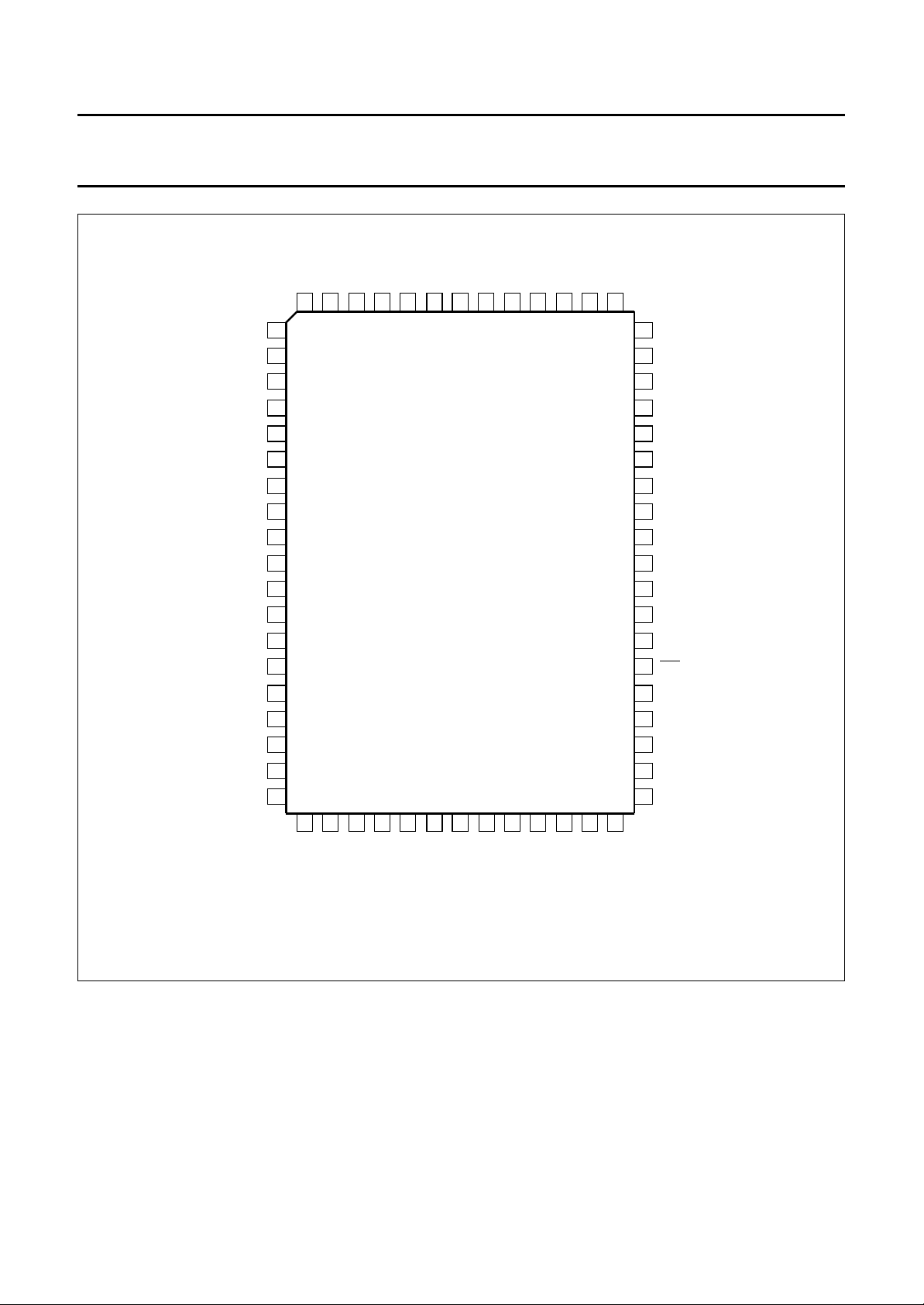
TYPE
NUMBER
NAME DESCRIPTION VERSION
PACKAGE
TDA1373H QFP64 Plastic quad flat package; 64 leads (lead length 1.95 mm);
body 14 × 20 × 2.7 mm; high stand-off height
DD
SOT319-1
V
1996 Jul 17 3
Page 4
Philips Semiconductors Product specification
General Digital Input (GDIN) TDA1373H
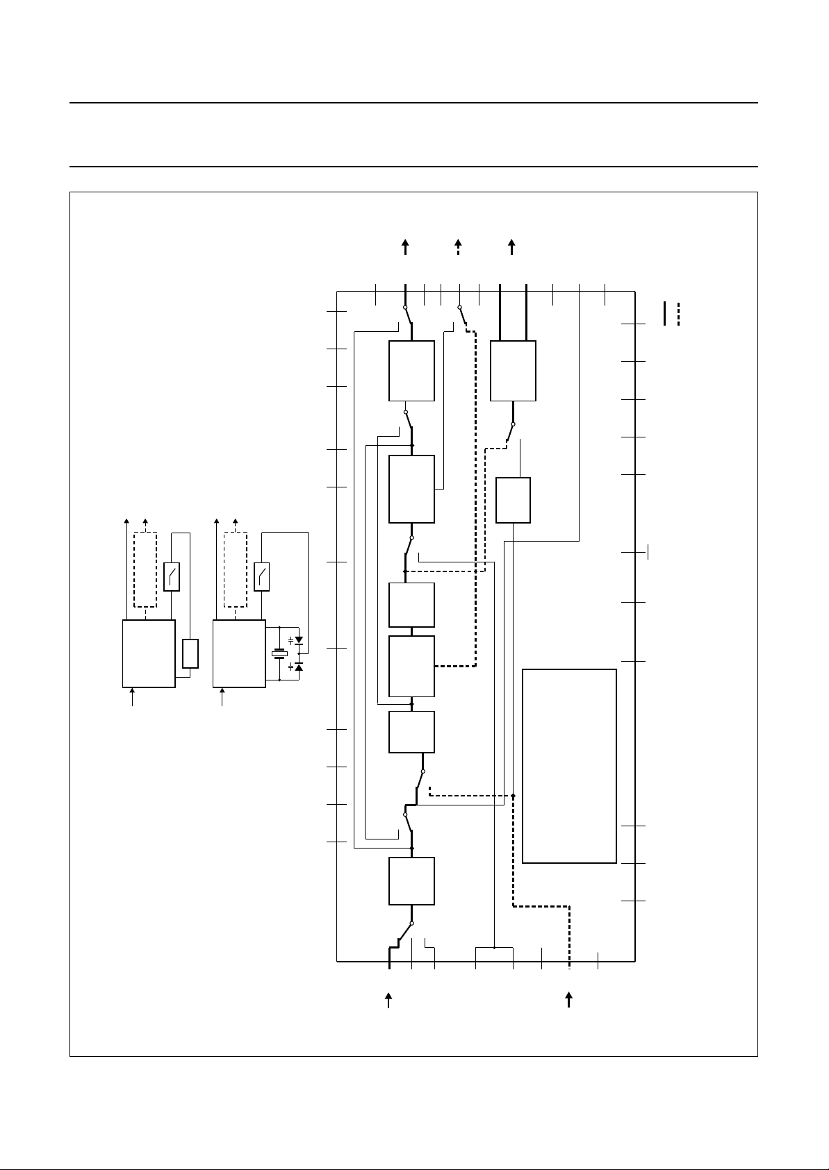
BLOCK DIAGRAM
V
SSA4
V
DDA4
CRYSTAL
OSCILLATOR
GENERAL
CONTROL
HOLD VCO
MM0
23 27 28 30 312221 19 204645473536345239 14327
MM1
CLO4CLO3CLO2CLO1CLIXTLOXTLIDA
so
768fso384fso256fso128f
CLOCK
SHOP
64f
so
25
FSL
handbook, full pagewidth
MU
EM
LOCK
SA
DI1D
DI1O
DI1S
V
DDA1
V
SSA1
DDDVDDDVDDD
V
DDD
DDDVDDD
11
44
37
48
43
62
63
1
DATA
SLICER
3
2
V
V
USER
CHANNEL
EXTRACTION
CHANNEL
EXTRACTION
DI2
STATUS
PHASE
DETECTOR
DI1
ADIC
(IEC 958
DECODER)
U
PV
C
WS
PO
LDCLCENCUSBS
MICRO-
CONTROLLER
INTERFACE/
STAND-ALONE
CONTROL
LOOP
FILTER
TST1
TST2
RST
AIL
AIR
42
41
38
4
5
stereo
FOD
FOS
2
I S OUT
55
FOC
FIFO
AND
GAIN
DNI
DI2
HOLD
2
I S IN
8
60
59
57
54
56
V
DI2C
DI2W
DI2D
FOW
SSD
V
12
SSD
32 x
DOWN-
SAMPLING
V
SSD
4 x
UP-
SAMPLING
SAMPLING
AOS
13 24
V
SSD
17
V
SSD
ATTENUATOR
4 x
DOWN-
16 x
UP-
SAMPLING
INS
VARIABLE
HOLD
IN-BAND
NOISE
SHAPER
BITSTREAM
DIGITAL
FILTER
DO2
DSO
2
I S
OUT
2
I S
OUT
DAC
OUTPUT
10
DO2D
16
DO2W
6
DO2C
50
DO1D
49
DO1W
51
DO1C
9
AOL1
15
AOR1
18
CLD
TDA1373H
33
40
26
29
V
V
SSD
V
SSD
SSD
53
58
61
64
V
SSD
V
V
SSD
SSD
SSDVSSD
MLC334 - 2
V
Switches MM1 and MM0 are controlled indirectly via the mode selection. All other switches can be controlled directly by the user.
Fig.1 Block diagram.
1996 Jul 17 4
Page 5
Philips Semiconductors Product specification
General Digital Input (GDIN) TDA1373H
PINNING
SYMBOL PIN DESCRIPTION TYPE
DI1S 1 IEC 958 digital audio input ‘S’ (200 mV peak-to-peak value) E036A
V
SSA1
V
DDA1
AIL 4 Bitstream audio input left HPP01
AIR 5 Bitstream audio input right HPP01
DO2C 6 serial digital audio output 2; bit clock output (192f
V
DDD
V
SSD
AOL1 9 Bitstream audio output left OPF40
DO2D 10 DLO = 0; serial digital audio output 2; data;
V
DDD
V
SSD
V
SSD
V
DDD
AOR1 15 Bitstream audio output right OPF40
DO2W 16 DLO = 0; serial digital audio output 2; word select output (4f
V
SSD
CLD 18 Bitstream DAC clock (192 or 128f
V
DDA4
V
SSA4
XTLI 21 crystal input 768f
XTLO 22 crystal output OSX01
CLI 23 external VCO input (SLAVE-VCO mode only) HPP01
V
SSD
FSL 25 SA = 0 (microcontroller operated) external VCO output (slave modes
V
SSD
CLO1 27 clock output 768f
CLO2 28 clock output 384f
V
SSD
CLO3 30 clock output 256f
CLO4 31 clock output 128f
V
DDD
V
SSD
BS 34 block sync; channel status/user channel/CD subcode OPF40
CEN 35 data enable; channel status/user channel/CD subcode OPF40
CUS 36 data bit; channel status/user channel/CD subcode OPF40
EM 37 IEC 958 source pre-emphasis flag OPF20
2 IEC 958 slicer analog ground E038A
3 IEC 958 slicer analog supply voltage E037A
) OPF40
so
7 digital supply voltage; note 1 −
8 digital ground; note 2 −
OPF40
DLO = 1; Bitstream audio output left inverted (
AOL1); note 3
11 digital supply voltage; note 1 −
12 digital ground; note 2 −
13 digital ground; note 2 −
14 digital supply voltage; note 1 −
);
so
OPF40
DLO = 1; Bitstream audio output right inverted (AOR1); note 3
17 digital ground; note 2 −
) OPF43
so
19 oscillator analog supply voltage E037A
20 oscillator analog ground E038A
so
OSX01
24 digital ground; note 2 −
HOF21
only); SA = 1 (stand-alone control) DI11 control line; note 4
26 digital ground; note 2 −
so
so
OPF40
OPF40
29 digital ground; note 2 −
so
; OPF40
so
OPF40
32 digital supply voltage; note 1 −
33 digital ground; note 2 −
1996 Jul 17 5
Page 6
Philips Semiconductors Product specification
General Digital Input (GDIN) TDA1373H
SYMBOL PIN DESCRIPTION TYPE
RST 38 power-on reset input (active LOW) HPP07
V
DDD
V
SSD
TST2 41 test pin 2 (LOW for normal operation) HPP01
TST1 42 test pin 1 (LOW for normal operation) HPP01
SA 43 Stand-alone/microcontroller operated selection;
MU 44 mute flag (active HIGH) OPF40
LD 45 SA = 0 (microcontroller operated) microcontroller interface; load
DA 46 SA = 0 (microcontroller operated) microcontroller interface (data);
CL 47 SA = 0 (microcontroller operated) microcontroller interface (clock);
LOCK 48 ADIC lock flag (active HIGH) OPF40
DO1W 49 serial digital audio output 1; word select input/output (f
DO1D 50 serial digital audio output 1; data OPF43
DO1C 51 serial digital audio output 1; bit clock input/output (48f
V
DDD
V
SSD
FOW 54 serial digital audio feature output; word select OPF43
FOD 55 serial digital audio feature output; data OPF43
FOC 56 serial digital audio feature output; bit clock (64f
DI2D 57 serial digital audio input 2; data HPP01
V
SSD
DI2W 59 serial digital audio input 2; word select HOF21
DI2C 60 serial digital audio input 2; bit clock output HOF21
V
SSD
DI1D 62 SA = 0 (microcontroller operated) IEC 958 digital audio input ‘D’ (CMOS
DI1O 63 IEC 958 digital audio input ‘O’ (CMOS level) HPP01
V
SSD
Notes
1. All V
2. All V
pins are internally connected.
DDD
pins are internally connected.
SSD
3. DLO is a command flag from register 4 (see Section “Command registers”).
4. SA is the stand-alone/microcontroller operated pin (pin 43). DI11, NSD, DI2, QU1, QU0 and MS0 are command flags
to control the operation of the device. For more information see Section “Controlling the GDIN”.
39 digital supply voltage; note 1 −
40 digital ground; note 2 −
HPP01
SA = 1 for stand-alone operation
HPP01
(read/write); SA = 1 (stand-alone control) NSD control line; note 4
HOF41
SA = 1 (stand-alone control) DI2 control line; note 4
HPP01
SA = 1 (stand-alone control) QU1/QU0 control line; note 4
) HOF41
so
) HOF41
so
52 digital supply voltage; note 1 −
53 digital ground; note 2 −
) OPF43
so
58 digital ground; note 2 −
61 digital ground; note 2 −
HPP01
level); SA = 1 (stand-alone control) MSO control line; note 4
64 digital ground; note 2 −
1996 Jul 17 6
Page 7
Philips Semiconductors Product specification
General Digital Input (GDIN) TDA1373H
handbook, full pagewidth
DI1S
V
SSA1
V
DDA1
DO2C
V
DDD
V
SSD
AOL1
DO2D
V
DDD
V
SSD
V
SSD
V
DDD
AOR1
DO2W
V
SSD
CLD
V
DDA4
AIL
AIR
SSD
V
DI1O
64
63
1
2
3
4
5
6
7
8
9
10
11
12
13
14
15
16
17
18
19
DI1D
62
SSD
V
61
DI2C
60
SSD
V
DI2W
59
58
TDA1373H
DI2D
57
FOC
56
FOD
55
FOW
54
SSD
V
53
DDD
V
52
51
DO1C
DO1D
50
49
DO1W
48
LOCK
CL
47
DA
46
45
LD
44
MU
SA
43
TST1
42
TST2
41
V
40
SSD
V
39
DDD
38
RST
EM
37
CUS
36
35
CEN
BS
34
V
33
SSD
20
21
SSA4
V
XTLI
22
XTLO
23
CLI
24
SSD
V
25
FSL
Fig.2 Pin configuration.
1996 Jul 17 7
26
V
SSD
27
CLO1
28
CLO2
29
SSD
V
30
CLO3
31
CLO4
32
DDD
V
MLB955 - 2
Page 8

Philips Semiconductors Product specification
General Digital Input (GDIN) TDA1373H
FUNCTIONAL DESCRIPTION
Operating modes
AMPLE RATE CONVERSION (SRC) MODE
S
The output sample rate is determined by a crystal and can
be chosen up to 49 kHz. The range of input sample rates
for a given output sample rate is given in Table 1. A pitch
variation (‘Varispeed’) of ±12% around the nominal input
sample rate can be tracked.
Table 1 Input sample rates
OUTPUT SAMPLE RATE
(kHz)
2
I
S INPUT (kHz)
0.3 to 1.7f
48 13 to 83 16 to 68
44.1 12 to 76 15 to 62
32 9to55 12to45
60
handbook, full pagewidth
THD N
(dB)
80
Data path
(see Fig.4)
The input signal at sample frequency fsi comes in via one
of the DI1 inputs (IEC 958) or via the serial input DI2X.
The signal passes through the FIFO/GAIN part and is
interpolated in the up-sampling filters. The actual sample
rate conversion takes place in the variable hold block. The
down-sampling filters decimate the sample frequency to
fso and after in-band noise shaping, the output signal is
present at serial output DO1. Additionally the converted
signal is available at the ‘analog’ Bitstream outputs AOL,
AOR and at the serial digital output DO2 (4f
).
so
IEC 958 INPUT (kHz)
so
0.35 to 1.45f
so
MLB956
100
120
140
160
10
Measurement done with ‘Audio Precision’.
SRC mode; 48 to 44.1 kHz; 20-bit output.
2
10
Fig.3 Total harmonic distortion plus noise as a function of frequency.
1996 Jul 17 8
3
10
4
10
f (Hz)
5
10
Page 9

Philips Semiconductors Product specification
General Digital Input (GDIN) TDA1373H
DO1C
DO1D
DO1W
DO2C
DO2D
DO2W
AOL
AOR
FOC
FOD
FOW
MLC335
Main path.
Example of
additional path.
TST2TST1CLIXTLIXTLOLOCKEMCUSCENBSFSL
DSO
DO2
CLD
2
digital output
digital input
analog output
fsoI S
DAC
BITSTREAM
TDA1373H
2
fsiAES/EBU or I S
e.g. TDA1547
so
768f
NOISE
IN-BAND
SHAPER
INS
DOWN-
SAMPLING
32 x AND 4 x
DNI
HOLD
VARIABLE
4 x AND 16 x
UP-SAMPLING
&
FIFO
GAIN
AOS
TDA1373H
FILTER
DIGITAL
BITSTREAM
HOLD
CS AND UC
DIGITAL PLL
EXTRACTION
CLO4CLO3CLO2CLO1RSTSAMUDALDCL
handbook, full pagewidth
Fig.4 Standard data path in the SRC mode.
DI2
FOS
ADIC
(IEC 958
DECODER)
DI1
DI1S
DI1O
DI1D
AIL
1996 Jul 17 9
AIR
INTERFACE
CLOCK SHOP
MICROCONTROLLER
DI2C
DI2D
GENERAL CONTROL
DI2W
Page 10

Philips Semiconductors Product specification
General Digital Input (GDIN) TDA1373H
SLAVE-VCO AND SLAVE-VCXO MODES
In the SLAVE-VCO and SLAVE-VCXO modes, the GDIN
can pass an exact copy of the incoming samples to the
output, e.g. for storage on a digital medium such as CD-R.
The output sample rate tracks any input sample rate within
the frequency range of the external VC(X)O (fso=fsi).
In the SLAVE-VCO mode a pitch variation of ±12.5%
around the nominal sample frequency can be tolerated.
Data path
The signal at input sample frequency fsi comes in via one
of the DI1 inputs (IEC 958).
The ADIC signal passes through the FIFO/GAIN block and
can be fed through the IN-BAND NOISE SHAPER to the
serial output DO1. Additionally, the signal is present at
DO2 (4fso) and at the Bitstream outputs AOL and AOR.
Exact copies for digital use (e.g. write to a disk) from the
input signal can be retrieved at output FO (this signal might
be affected by jitter since it has not passed through the
FIFO/GAIN block). By means of data path switch DSO, this
direct output of the ADIC block can also be fed to
output DO1. Note that in this event the DO1 serial format
becomes equal to the FO format (see Table 3).
(see Fig.5)
AD/DA
In this mode, the GDIN supports an economic realization
of analog-to-digital and digital-to-analog conversion, in
accordance with the Bitstream principle. This requires a
Bitstream sigma-delta modulator and a Bitstream DAC,
since the up-sampling and down-sampling filters of the
sample rate convertor are reused. ADC and DAC can be
simultaneously performed.
Data path DA conversion
The signal at sample frequency fso comes in via serial input
DI2X or via one of the DI1 inputs (IEC 958). The signal
passes through the FIFO/GAIN part and is interpolated in
the up-sampling filters. A Bitstream digital filter converts
this signal into a Bitstream signal at outputs AOL and AOR,
after which it can be filtered by a Bitstream DAC like the
TDA1547.
Data path AD conversion
The Bitstream signal from the sigma-delta modulator
enters the GDIN at inputs AIL and AIR. The
down-sampling filters decimate this signal to fso and after
in-band noise shaping (selectable), the output signal is
present at serial output DO1.
MODE
(see Fig.6)
(see Fig.6)
1996 Jul 17 10
Page 11
Philips Semiconductors Product specification
General Digital Input (GDIN) TDA1373H
DO1C
DO1D
DO1W
DO2C
DO2D
DO2W
AOL
AOR
FOC
FOD
FOW
MLC336
Main path.
Example of
additional path.
TST2TST1CLIXTLIXTLOLOCKEMCUSCENBSFSL
DSO
DO2
CLD
2
digital output
analog output
fsiI S
BITSTREAM
TDA1373H
2
digital input
fsiAES/EBU or I S
digital output
fsiI S
DAC e.g.TDA1547
VCO
digital input
2
analog output
BITSTREAM
DAC e.g.TDA1547
TDA1373H
2
fsiAES/EBU or I S
so
768f
NOISE
IN-BAND
SHAPER
INS
DOWN-
SAMPLING
32 x AND 4 x
DNI
HOLD
VARIABLE
4 x AND 16 x
UP-SAMPLING
&
FIFO
GAIN
DI2
TDA1373H
FILTER
DIGITAL
BITSTREAM
AOS
HOLD
CS AND UC
DIGITAL PLL
CLO4CLO3CLO2CLO1RSTSAMUDALDCL
handbook, full pagewidth
EXTRACTION
FOS
ADIC
DI1
DI1S
1996 Jul 17 11
(IEC 958
DECODER)
DI1O
DI1D
AIL
AIR
INTERFACE
CLOCK SHOP
MICROCONTROLLER
DI2C
DI2D
GENERAL CONTROL
Fig.5 Standard data path in the SLAVE-VCO and SLAVE-VCXO modes.
DI2W
Page 12

Philips Semiconductors Product specification
General Digital Input (GDIN) TDA1373H
2
digital output
fsoI S
TDA1373H
analog output
DAC
BITSTREAM
e.g. TDA1547
so
768f
TST2TST1CLIXTLIXTLOLOCKEMCUSCENBSFSL
DO1C
AD OUT
DO1D
DSO
NOISE
IN-BAND
SHAPER
INS
DOWN-
SAMPLING
32 x AND 4 x
DNI
HOLD
VARIABLE
DO1W
DO2C
DO2D
DO2
DO2W
DA OUT
AOL
AOR
FILTER
DIGITAL
BITSTREAM
AOS
HOLD
FOC
FOD
FOW
MLC337
Main path.
CLD
CLO4CLO3CLO2CLO1RSTSAMUDALDCL
Example of
additional path.
handbook, full pagewidth
4 x AND 16 x
UP-SAMPLING
ADC
BITSTREAM
e.g. SAA7360
digital input
analog input
2
fsoAES/EBU or I S
DI1S
DA IN
FOS
FIFO
ADIC
DI1
&
GAIN
DI2
(IEC 958
DECODER)
DI1O
DI1D
1996 Jul 17 12
TDA1373H
AIL
AD IN
AIR
CS AND UC
DIGITAL PLL
INTERFACE
CLOCK SHOP
MICROCONTROLLER
DI2C
DI2D
EXTRACTION
Fig.6 Standard data paths in the AD/DA mode.
GENERAL CONTROL
DI2W
Page 13

Philips Semiconductors Product specification
General Digital Input (GDIN) TDA1373H
Description of functional blocks
IEC 958
AUDIO DIGITAL INPUT CIRCUIT
The TDA1373H has three IEC 958 inputs:
1. DI1S.
2. DI1O.
3. DI1D.
DI1S accepts IEC 958 line signals (minimum 200 mV
ADIC locks in less than 1 ms for a 44.1 kHz input signal.
During this lock-in time the word clock is stopped and the
audio bits are muted.
The validity flag (VA), pre-emphasis flag and pin (EM), lock
flag (LCK) and lock pin (LOCK) are available to check the
status of the ADIC. This validity flag is an OR-ing of the
incoming validity (V) bit and the own error detection of the
ADIC. The actions which take place in case of detected
errors are listed in Table 2.
peak-to-peak value and maximum 5 V peak-to-peak
value), DI1O and DI1D accept only CMOS level signals.
The input sample rate range that can be handled depends
on the output sample frequency (fso) of the device.
The maximum useful word length of the incoming samples
is 20 bits.
The internal ADIC retrieves the stereo audio samples, the
V, U, C and P data bits, the ADIC word clock and the bit
clock from the selected IEC 958 input signal. The digital
SERIAL DIGITAL INPUTS DI2W, DI2D AND DI2C
The serial digital input DI2 can be used as standard input
instead of the DI1 IEC 958 input or can be used together
with the FO-output to switch a DSP IC in the input data
path. A third possibility is to use DI2 as direct input to the
GDIN Bitstream digital filter. In that case the DI2 input
signal should be 4× oversampled externally. The serial
formats supported are shown in Fig.7 and Table 3.
Table 2 Error concealment in the IEC 958 decoder
ERROR ACTION DATA ACTION WORD CLOCK
Validity (V-bit) error pass sample no action
Parity (P-bit) error repeat last correct sample
Number of data bits ≠32
Missing pre-amble(s)
Extra pre-amble(s)
More than 4 pre-ambles missing or extra mute output; restart stop ADIC word clock
Table 3 Serial input and output formats (see note 1)
INPUT
OUTPUT
DI2 f
DO1 f
DO2 4f
FO f
f
WS
si
4f
so
so
so
si
f
BCK
≤128f
192f
48f
≤128f
192f
64f
I2S
si
so
so
so
so
so
JAPANES
E 16-BIT
JAPANESE
18-BIT
S S S S no DI2, DI21 and DI22
M S S S no DI2
MM M
S −−
MM M − no DO2, DO21 and DO22
M −− −yes FO and FO1
Note
1. S = slave; M = master.
1996 Jul 17 13
JAPANESE
20-BIT
3-STATE CONTROL BITS
− yes DO1S, DO1 1 and DO12
Page 14

Philips Semiconductors Product specification
General Digital Input (GDIN) TDA1373H
handbook, full pagewidth
DATA
LSB MSB LSB MSB
BCK
WS
WS (W)
BCK (C)
DATA (D)
RIGHT RIGHT
LEFT
t
t
HB
r
t
LB
t
f
T
BCK
t
hWS
t
suWS
LEFT
t
suDATthDAT
LSB MSB
LEFT
RIGHT
a.
LEFT
DATA
BCK
WS
a. I2S input format.
b. Japanese input format.
WS (W)
t
r
RIGHT
t
HB
t
LB
t
f
t
hWS
t
suWS
BCK (C)
T
BCK
DATA (D)
MSB LSB MSB
LSB MSB
LEFT
b.
Fig.7 Timing diagram for the serial input and output formats.
t
suDATthDAT
RIGHT
LSB
MLB960
1996 Jul 17 14
Page 15

Philips Semiconductors Product specification
General Digital Input (GDIN) TDA1373H
SERIAL DIGITAL OUTPUTS DO1W, DO1D AND DO1C
Depending on the operating mode and data path
switching, DO1 can contain the output of the in-band noise
shaper or can be directly connected to the output of the
internal ADIC. The supported serial formats and modes of
this interface are given in Table 3.
In case the GDIN goes out-of-lock the output data is muted
and if the output is configured as master transmitter, the
word clock slips half a word clock period. If this is
undesirable, use the serial output as a slave transmitter.
S
ERIAL DIGITAL OUTPUTS DO2W, DO2D AND DO2C
The additional digital audio output DO2 operates at 4fso.
DO2 can contain data of the up-sampling (not in SRC
mode) or down-sampling filters. The formats supported
are shown in Table 3.
ERIAL FEATURE OUTPUTS FOW, FOD AND FOC
S
The internal ADIC output is directly available in I2S format
at this output. This makes it possible to switch a DSP
featuring IC in the data path before SRC (at f
). See
si
Table 3 for the formats supported.
BITSTREAM INPUTS AIL AND AIR
The Bitstream input receives data at 128fso from a 1-bit
sigma-delta modulator. Possible Bitstream inputs at 64f
so
are held twice. The timing diagram for the Bitstream inputs
and outputs is given in Fig.8.
B
ITSTREAM OUTPUTS AOL1 AND AOR1
The Bitstream output generates a 128 (SRC and SLAVE
modes) or 192 (AD/DA mode) times oversampled
Bitstream and can be connected to a Bitstream DAC (e.g.
TDA1547) for high-quality DAC. It is also possible to get
the inverted Bitstream signals on the complementary
Bitstream outputs AOL1 (pin DO2D) and AOR1
(pin DO2W) by setting the DLO control bit. By using a
simple low-pass filter, this symmetrical Bitstream output
can be used to make an inexpensive analog monitor
output. In that event the serial digital output DO2 cannot be
used.
handbook, full pagewidth
FOC, CLO4 and DO2C
CLOCK
AIL and AIR
DATA
CLD
CLOCK
AOL1, AOL2,
AOR1 and AOR2
DATA
Fig.8 Timing diagram for the Bitstream inputs and outputs.
t
d1
T
t
f
cy
t
r
t
t
d2
CH
t
d3
V 1 V
1.0 V
DD
t
CL
MLB961
1996 Jul 17 15
Page 16

Philips Semiconductors Product specification
General Digital Input (GDIN) TDA1373H
FIRST-IN FIRST-OUT (FIFO)
The incoming samples are buffered in a FIFO. The depth
of this FIFO determines the transients that can be allowed
in the input frequency, as they may occur during pitch
control. The FIFO has a depth of 8 samples, which makes
GDIN support a tracking speed of up to 4 kHz/ms. FIFO
overflow detection is provided to detect out-of-lock
situations.
G
AIN CONTROL
At the begin of the data path, the signal level can be
controlled over a gain/attenuation range from 2 to 0 with a
step size of 2E-7. This gain control can be used for volume
control, gain correction and fade-in or fade-out. For normal
operation, the gain level should be set to 1-2E-7
(−0.068 dB) to avoid pass band ripple clipping in the digital
filters. Whenever a new gain value is set, the gain level is
increased or decreased by one step per input sample until
the new entered value is reached.
Setting the MMU control bit forces the GDIN to start a soft
muting. The gain is decreased, by one step per input
sample, to zero. Clearing the MMU bit will increase the
gain back to its original value. Only those outputs, for
which the signal passes through the ‘gain control’ part, are
muted.
as the up-sampling filter for a Bitstream digital-to-analog
conversion in the AD/DA mode, in combination with the
Bitstream digital filter and Bitstream DAC (e.g. TDA1547).
Two filter characteristics can be chosen by the control bit
SS (see Table 4).
The 50 dB stop band suppression mode is especially
suited for 32 kHz input sources like Digital Satellite Radio
(DSR), where a very narrow transition band is required to
obtain 0 to 15 kHz pass band.
VARIABLE HOLD
In SRC mode, the variable hold is the interface between
the 64× up-sampling filters (64fsi) and the
128× down-sampling filters (128fso). In SLAVE and AD/DA
modes, the variable hold holds each sample twice from
64fsito 128fsi (fsi=fso).
128×
DOWN-SAMPLING FILTER (see Fig.10)
After SRC, a 128× (32× +4×) down-sampling filter
decimates the signal to fso. In the AD/DA mode, this filter
is used as the ADC down-sampling filter for a Bitstream
sigma-delta modulator. The stop band suppression is
80 dB from 0.54648fso (e.g. 24.1 kHz at fso= 44.1 kHz).
UP-SAMPLING FILTER
64×
A 64× (4× and 16×) oversampling filter is incorporated in
the GDIN for the SRC process. This filter can also be used
Table 4 Filter characteristics 64× up-sampling filter
SS PASS BAND STOP BAND
0 0 to 0.45351f
1 0 to 0.46875f
si
si
±0.004 dB 0.54648fsito 1f
±0.004 dB 0.53125fsito 1f
si
si
−70 dB
−50 dB
1996 Jul 17 16
Page 17

Philips Semiconductors Product specification
General Digital Input (GDIN) TDA1373H
stop band
(dB)
100
0
20
40
60
80
0 20406080
handbook, full pagewidth
suppression
SS = 0; 70 dB stop band suppression.
Fig.9 Filter characteristic 64× up-sampling filter.
f (kHz)
MLB962
100
stop band
(dB)
100
0
20
40
60
80
0 20406080
handbook, full pagewidth
suppression
Fig.10 Filter characteristic 128× down-sampling filter.
f (kHz)
MLB963
100
1996 Jul 17 17
Page 18

Philips Semiconductors Product specification
General Digital Input (GDIN) TDA1373H
IN-BAND NOISE SHAPING (INS)
The standard 20-bit output word length can be reduced to
16 or 18 bits to match digital consumer equipment.
Normally 16 bit output re-quantization at audio-band
sample rates drops the signal-to-noise ratio (S/N)
inevitably to 95 dB, because of the re-quantization noise at
−98 dB.
It is possible however to shape the re-quantization noise in
a psycho-acoustical way. This reduces the re-quantization
noise at the frequencies where the human ear is most
sensitive and stores the bulk of re-quantization noise at
high frequencies, where the human ear is quite insensitive.
The In-band Noise Shaping function (to 16 or 18 bits)
results in a subjective quality improvement of about 2 bits
below the actual quantization level.
It is also possible to re-quantize the 20 bit output to 16 bits
without noise shaping but by a simple rounding operation.
Table 5 gives an overview of the 4 possible settings.
Table 5 Selectable output word lengths
QU1 QU0 WORD LENGTH
0 0 16 bit (rounded)
0 1 20 bit
1 0 16 bit INS
1 1 18 bit INS
(1)
(1)
Note
1. INS = In-band Noise Shaping.
ITSTREAM DIGITAL FILTER
B
The Bitstream digital filter generates a Bitstream signal
which should be filtered by a Bitstream DAC
(e.g. TDA1547) to become a high-quality analog signal.
The input for this block can be selected from the output of
the up-sample path or directly from serial input DI2. In this
case, the input signal applied to DI2 should be externally
oversampled to 4fso and further oversampling will be
carried out by the hold function. The Bitstream signal has
a frequency of 128fso (SRC and SLAVE modes) or 192f
so
(AD/DA mode).
To prevent idle patterns in the audio band, it is strongly
advised to add out-of-band dither by setting
control bit NSD.
IGITAL PLL
D
allows fast locking to the input frequency and a small
bandwidth during steady-state. At start-up, the bandwidth
of the 3-step digital loop filter is gradually reduced to
0.5 Hz. A difference frequency of 1 Hz is reached within
512 input samples (10 ms at 44.1 kHz), which allows to
start the SRC. At this moment the outputs are de-muted,
indicated at pin MU and status flag MUT.
The FIFO position is continuously monitored to control the
adaptive loop filter. The loop filter switches back to a fast
state when the FIFO tends to drift, e.g. during pitch control
on the input signal. It is possible to fix the loop filter in one
of the three states. In the adaptive mode, the actual state
can be monitored by the microcontroller (ST1 and ST0). In
SRC mode, the microcontroller can retrieve the exact input
sample frequency via the status registers STS3 and STS4.
Table 6 PLL operation modes
LC1 LC0
PLL
OPERATION
PLL BANDWIDTH
(Hz)
0 0 adaptive 500, 50 or 0.5
0 1 state 1 fixed 500
1 0 state 2 fixed 50
1 1 state 3 fixed 0.5
In both SLAVE modes, a pulse modulated signal at
pin FSL is present to control the external VC(X)O. In
SLAVE-VCO mode, CLI is the clock input of the GDIN and
in SLAVE-VCXO mode XTLI is the clock input. An external
1000 Hz low-pass filter retrieves the control voltage for the
VC(X)O. To get the loop characteristics as described
above, the centre frequency of the VCO should be at
1
⁄2VDD and the sensitivity should be:
768f
=
------------------------ 1
-- 2
so c()
V
DD
Hz/V.
g
v
The maximum VCO frequency range is:
(768 × 0.3)f
IEC 958 C
< 768fsi(=fso) < (768 × 1.7)f
so(c)
HANNEL STATUS AND USER CHANNEL EXTRACTOR
so(c)
(49 kHz).
(CUP)
The internal ADIC retrieves also the Channel Status (CS)
and User Channel (UC) bits from the IEC 958 signal. The
C/U processing function block can be programmed for
4 different functions (see Table 7).
The digital PLL controls the variable hold function which
steers the actual SRC process. An adaptive loop filter
1996 Jul 17 18
Page 19

Philips Semiconductors Product specification
General Digital Input (GDIN) TDA1373H
Table 7 Overview of selectable CUP functions
SM1 SM0 LR
0 1 0 extract full C-block left (192 bits/block) 80H to 97H
0 1 1 extract full C-block right (192 bits/block) 80H to 97H
1 0 X extract full U-block (384 bits/block) 80H to AFH
0 0 X decode CD-Subcode Q-information (80 bits/CD frame) from U-bits 80H to 89H
Note
1. X = don’t care.
(1)
CUP FUNCTION RAM BUFFER
The extracted or decoded information can be read in three
ways:
• From the internal RAM buffer by a microcontroller
(see Section “The RAM buffer”)
• At the output pins CUS, BS and CEN (see Fig.11)
• In status registers STS5 and STS6 (permanent 16
‘consumer mode’ C-bits, see Table 9).
During CD subcode Q extraction, a 16-bit CRC is done
over the Q-channel (CRC flag). This flag is only
meaningful when the ADIC is locked (LCK flag).
T
HE RAM BUFFER
A double RAM buffer is present in the device. While
reading one buffer, the other buffer is filled with the new
incoming data. The RAM buffer can be read in two ways:
1. Interrupt protocol (UIP = 0).
2. User request protocol (UIP = 1).
Interrupt protocol (UIP = 0)
A C-block, a U-block or CD Subcode frame is read in the
time between two Block Sync (output pin BS) pulses,
which can be used as the interrupt for a microcontroller. At
a sample rate of 44.1 kHz, the microcontroller must be
able to read a C-block or U-block within
CD Subcode frames are received at a data rate of 75 Hz
or 13.3 ms/frame.
192
---------------44100
4.35 ms.=
User request protocol (UIP = 1)
The microcontroller requests for a C, U and CD-Q block or
frame, which will then become available at the next block
preamble, indicated by BS. The information is not updated
until the next user request, which means the
microcontroller can take any time to read the information.
The CD Subcode CRC check flag always shows the CRC
over the last received CD Subcode Q frame and is not
stored with the present Q frame in the buffer. Figure 12
shows the user request read procedure.
1996 Jul 17 19
Page 20

Philips Semiconductors Product specification
General Digital Input (GDIN) TDA1373H
T
handbook, full pagewidth
BS
cyBS
t
suBC
CEN
t
suCC
CUS
BS
CEN
CUS
t
HBS(CD)
t
hBC
t
hCC
t
suCC(CD)
LEFT CS0
or UC0
t
LCEN
RIGHT CS0
or UC1
LEFT CS191
or UC382
t
cyCEN
RIGHT CS191
or UC 383
a.
t
suBC(CD)
t
hCC(CD)
Q1 R1 S1 Q98 Q1 R1 S1
T
cyBS(CD)
t
HCEN(CD)
t
cyCEN
b.
a. Channel Status (CS) or User Channel (UC) extraction.
b. CD subcode demodulation.
Fig.11 Timing of the CUS, CEN and BS output pins.
1996 Jul 17 20
MLB964
Page 21

Philips Semiconductors Product specification
General Digital Input (GDIN) TDA1373H
handbook, full pagewidth
Block Sync or
CD subcode frame sync (BS)
Buffer Contents Valid (BCV)
OK, buffer valid
Set Buffer Free (SBF)
request to read (hold buffer)
microcontroller
data communication
(LD, CL, DA)
start to
read
buffer
Fig.12 C, U and CD-Q user request procedure.
THE MICROCONTROLLER INTERFACE/
STAND-ALONE CONTROL BLOCK
If pin SA is LOW, a microcontroller controls and monitors
the operation of the GDIN and reads C, U and CD-Q
information. A 3-line bidirectional serial interface with data
(DA), load (LD) and clock (CL) line is present. For both a
write and read operation the microcontroller generates the
clock and load signals.
A single byte is written by setting the LD signal active
HIGH during transmission of the serial data. At the rising
edge of the serial clock, the GDIN clocks in the serial data.
At the end of the 8-bit data word a ‘load pulse’ should be
given to enable the internal serial-to-parallel conversion.
Write operations are always two-byte operations. First, the
register address is sent to the GDIN, then the
corresponding data is send (see Fig.13):
1. Write Address.
2. Write Data byte.
A single byte read-operation is initialized by pulling LD
LOW. When the serial clock is started, the GDIN will
transmit serial data on the DA line. The information is read
by the microcontroller at the rising edges of the clock CL.
set buffer free again
MLB965
buffer
completely
read
Read operations are at least two-byte operations with
multi-byte reads possible. The address is sent to the GDIN
and then one or more bytes are read from the GDIN with
each additional byte coming from an incrementally higher
address:
1. Write Address.
2. Read Data byte.
3. Read Data byte.
4. Read Data byte.
5. Etc.
Multi-read operations continue to cycle through the given
Register Address Range until the read operation is
completed.
If pin SA is HIGH, the GDIN can operate without an
external microcontroller. In this event, only the SRC mode
and the AD/DA mode can be selected. A number of pins
are reconfigured to control some of the internal switches of
the device. For more information see Chapter “Pinning”
and Section “Controlling the GDIN”.
1996 Jul 17 21
Page 22

Philips Semiconductors Product specification
General Digital Input (GDIN) TDA1373H
Table 8 TDA1373H memory map
REGISTER ADDRESS RANGE REGISTER NAME TYPE
00H to 05H CMD1 to CMD6 command; read/write
40H to 45H STS1 to STS6 status; read
80H to 97H RAM buffer; C-block read
80H to AFH RAM buffer; U-block read
80H to 89H RAM buffer; CD-Q frame read
handbook, full pagewidth
CL
LD
t
suDC
DA
CL
T
cy
t
hDC
7070
t
LCL
t
HCL
t
hLC
t
suLC
t
LD1
a.
t
HLD
LD
DA
7070
b.
a. A complete write operation.
b. A complete read operation.
Fig.13 Timing for the microcontroller read and write operations.
1996 Jul 17 22
t
suLC
t
t
suDC
hDC
MLB966
Page 23

Philips Semiconductors Product specification
General Digital Input (GDIN) TDA1373H
Controlling the GDIN
M
ICROCONTROLLER OPERATED
Status registers
Table 9 Status registers
REGISTER BIT FLAG DESCRIPTION EXPLANATION
STS1 (40H) GDIN
status information
STS2 (41H) GDIN
status information
STS3 (42H) 7 to 0 LF15 to LF8 LF15 to LF0:
STS4 (43H) 7 to 0 LF7to LF0
STS5 (44H)
(6)
AES/EBU channel
status
STS6 (45H)
(6)
AES/EBU channel
status
7 − reserved −
6 − reserved −
5 − reserved −
4 − reserved −
3 LCK internal ADIC lock status 0 = not locked; 1 = locked
(1)
2 CRC CD-Q channel; CRC check
1 VA validity bit
(2)
0 = OK; 1 = error
0 = valid; 1 = not valid
0 BCV RAM buffer contents 0 = valid; 1 = not valid
7 − reserved −
6 − reserved −
5 − reserved −
4 − reserved −
3 − reserved −
2 and 1 ST1 and ST0 PLL operating status
(3)
00 = reserved; 01 = state 1;
10 = state 2; 11= state 3
0 MUT mute status
(4)
0 = mute OFF; 1 = mute ON
fsi=fso× (1 − (0.75 × LF15 to LF0))
input sample rate
(5)
7 and 6 CA1 and CA0 clock accuracy 00 = level 2; 01 = level 1;
10 = level 3; 11= reserved
5 and 4 FS1 and FS0 input sample rate 00 = 44.1 kHz; 01 = reserved;
10 = 48 kHz; 11= 32 kHz
3 EM pre-emphasis 0 = OFF; 1 = ON
2 CPY copyright protection 0 = YES; 1 = NO
1 AN audio or data 0 = audio; 1 = data
0 CPF consumer or professional use 0 = consumer; 1 = professional
7 CAT7 CAT7 to CAT0: category code some examples:
6CAT6
5CAT5
4CAT4
3CAT3
2CAT2
1CAT1
0CAT0
(7)
00000000 = general
10000000 = CD
1100001L = DCC
1100000L = DAT
0100100L = mixer
0101100L = SRC
1001000L = MD
Notes
1. Only valid when the internal ADIC is in lock (bit 3 of register STS1; LCK = 1).
1996 Jul 17 23
Page 24

Philips Semiconductors Product specification
General Digital Input (GDIN) TDA1373H
2. VA = IEC 958 V-bit or ADIC error detector.
3. Only valid when the digital PLL works in adaptive mode.
4. After approximately 512 stereo input samples (approximately 10 ms when fsi= 44.1 kHz).
5. Only valid in SRC mode. LF15 to LF0 are in two’s complement notation.
6. Only valid when IEC 958 input format is consumer (bit 0 of register STS5; CPF = 0). When the input format is
professional (CPF = 1) the STS5 and STS6 registers contain the first 16 bits of C-block.
7. Generation status (L-bit).
Command registers
Table 10 Command registers
REGISTER BIT FLAG DESCRIPTION EXPLANATION
CMD1 (00H) ADIC
control
CMD2 (01H) loop
and mode control
CMD3 (02H)
data path
(5)
7 and 6 DI12 and DI11 ADIC input selector 00 = DI1S; 01 = DI1O;
10 = DI1D; 11 = reserved
5 UIP user interface protocol 0 = interrupt;
1 = user requirement
4 SBF set internal RAM buffer free 0 = hold buffer;
1 = set buffer free
3 and 2 SM1 and SM0 channel decoding 00 = CD-Q; 01 = C-block;
10 = U-block; 11 = reserved
1 LRS C-block left/right selector 0 = left; 1 = right
0 DBA RAM buffer mode 0 = normal; 1 = test
7 − reserved −
6 − reserved −
5 and 4 LC1 and LC0 PLL control; note 1 00 = adaptive;
01 = state 1 fixed;
10 = state 2 fixed;
11 = state 3 fixed
3 and 2 MS1 and MS0 mode selector; notes 1 and 2 00 = SRC mode;
01 = AD/DA mode;
10 = SLAVE-VCXO mode;
11 = SLAVE-VCO mode
1 RTR enable 3-state outputs; note 3 0 = 3-state; 1 = enabled
0 MRS reset (hardware reset); note4 0 = no reset; 1 = reset
7 DSO DO1 output selector 0 = INS; 1 = ADIC
6 − reserved −
5 FOS FO output selector 0 = ADIC; 1 = 128× filter
4 DI2 FIFO input selector 0 = FOW, FOD and FOC;
1 = DI2W, DI2D and DI2C
3 DNI input selector 128× filter 0 = variable hold; 1 = AIL/AIR
2 INS In-band Noise Shaper input
selector
1 AOS Bitstream digital filter input
selector
0 DO2 DO2 output selector 0 = 128× down; 1 = 64× up
0 = output 128× down;
1 = output FIFO/GAIN
0 = variable hold;
1 = DI2W, DI2D and DI2C
1996 Jul 17 24
Page 25

Philips Semiconductors Product specification
General Digital Input (GDIN) TDA1373H
REGISTER BIT FLAG DESCRIPTION EXPLANATION
CMD4 (03H)
control
CMD5 (04H)
input/output
formats
CMD6 (05H) 7 GAIN7 GAIN7 to GAIN0: gain of the
7 − reserved −
6 − reserved −
5 MMU soft mute function; note 7 0 = OFF; 1 = ON
4 and 3 QU1 and QU0 in-band noise shaper 00 = 16-bit; 01 = 20-bit;
10 = 16-bit INS; 11= 18-bit INS
2 NSD dither Bitstream digital filter;
0 = OFF; 1 = ON
note 8
1 DLO symmetrical Bitstream output 0 = OFF; 1 = ON
0 SSP stop band suppression 64× filter;
0 = 70 dB; 1 = 50 dB
note 9
2
7 and 6 DI22 and DI21 serial format DI2 input 00 = I
S; 01 = Japanese 16-bit;
10 = Japanese 18-bit;
11 = Japanese 20-bit
2
5 and 4 DO22 and
DO21
serial format DO2 output 00 = I
S; 01 = Japanese 16-bit;
10 = Japanese 18-bit;
11 = reserved
2
3 and 2 DO12 and
DO11
serial format DO1 output 00 = I
S; 01 = Japanese 16-bit;
10 = Japanese 18-bit;
11 = 3-stated
1 DO1M DO1 master/slave selector 0 = master; 1 = slave
2
0 FOT FO output 3-state selector 0 = I
S; 1 = 3-stated
some examples:
6 GAIN6
5 GAIN5
4 GAIN4
GCM block
step =1⁄
128
; maximum = 2;
11111111 = ×2 (maximum)
10000000 = ×1
01111111 = ×0.992
00000001 = ×0.0078
(10)
3 GAIN3
2 GAIN2
1 GAIN1
0 GAIN0
Notes
1. In the SLAVE-VCXO mode, the PLL should be fixed in state 2 until locked.
2. A mode change will always invoke a restart of the GDIN.
3. At power-on the DO1 and FO outputs are ‘3-state’ to avoid I2S bus conflicts. This bit overrides the serial I/O
control bits.
4. A MRS or hardware reset clears all command registers, also the MRS flag itself.
5. See Section “Data path switching” for possible settings of the data path switches in the different modes.
6. Set all reserved flags to 0.
7. Setting MMU starts a soft-mute from current gain value to 0 by1⁄
per input sample. Clearing MMU starts the
128
inverse process from 0 to current gain value.
8. To prevent idle patterns in the audio band, it is strongly advised to add out-of-band dither by setting control bit NSD.
9. Set this bit for 32 kHz input sources.
10. Use ‘01111111’ for normal operation to avoid pass band ripple clipping.
1996 Jul 17 25
Page 26

Philips Semiconductors Product specification
General Digital Input (GDIN) TDA1373H
Data path switching
All data path switches are freely controllable, although not all combinations make sense in the different operating modes.
Table 11 shows the preferred settings of the CMD3 control register.
Table 11 Preferred settings of the CMD3 control register
REGISTER BIT FLAG DATA PATH SWITCH SRC
CMD3 (02H)
data path
7 DSO DO1 output selector; note 2 0 A A
6 − reserved −−−
5 FOS FO output selector; note 2 A A A
4 DI2 FIFO input selector A A A
3 DNI input selector 128× filter 0 1 1
2 − reserved −−−
1 AOS AOL and AOR output selector A A A
0 DO2 DO2 output selector 0 A A
(1)
SLAVE
(1)
AD/DA
(1)
Notes
1. Level 0 or 1 indicates to set the flag in this position. A = application dependent.
2. When the output of the internal ADIC is fed directly to DO1 or FO, the serial output format is I
2
S, the word select
jitters (by one 384fso clock cycle) and the number of bit clocks per word select is not fixed.
TAND-ALONE CONTROL
S
When pin SA is HIGH, the GDIN operates under stand-alone control. Some basic settings can be controlled in this event
by changing the level at the control pins. Table 12 shows which command bits are pin-controllable during stand-alone
operation. The command bits which are not pin-controllable are automatically set to their appropriate value in accordance
with the selected mode (SRC or AD/DA). All control bits not shown get the value 0 in the event of stand-alone control.
Table 12 Command registers
REGISTER FLAG PIN DESCRIPTION EXPLANATION
CMD1 (00H) ADIC
control
CMD2 (01H) loop
and mode control
DI11 FSL ADIC input selector 0 = DI1S;
1 = DI1O
MS0 DI1D mode selector; note 1 0 = SRC mode;
1 = AD/DA mode
RTR − enable 3-state outputs; note 2 RTR is always 1 in stand-alone
mode
CMD3 (02H)
data path
DI2 DA FIFO input selector 0 = FOW, FOD and FOC;
1 = DI2W, DI2D and DI2C
DNI − input selector 128× filter SRC mode = 0: variable hold;
AD/DA mode = 1: AIL/AIR
CMD4 (03H)
control
QU0/QU1 CL in-band noise shaper 0 = 20 bit; 1 = 16 bit INS
NSD LD dither Bitstream digital 0 = OFF; 1 = ON
CMD6 (05H) GAIN − gain of the FIFO/GAIN block gain = 01111111 = ×0.992
Notes
1. When the device operates in stand-alone control, only the SRC mode and AD/DA mode are available.
2. This means that all 3-state outputs are permanently enabled during stand-alone operation.
1996 Jul 17 26
Page 27

Philips Semiconductors Product specification
General Digital Input (GDIN) TDA1373H
LIMITING VALUES
In accordance with the Absolute Maximum Rating System (IEC 134).
SYMBOL PARAMETER CONDITIONS MIN. TYP. MAX. UNIT
V
DD
I
DD
V
i
I
i(max)
I
o(max)
P
tot
T
stg
T
amb
V
es
Notes
1. Human Body Model (HBM): C = 100 pF; R = 1.5 kΩ; 3 zaps positive and 3 zaps negative.
2. Machine Model (MM): C = 200 pF; L = 2.5 µH; R = 25 Ω; 3 zaps positive and 3 zaps negative.
supply voltage −0.5 − +6.5 V
supply current −−200 mA
input voltage −0.5 − VDD+ 0.5 V
maximum input current −−10 mA
maximum output current −−10 mA
total power dissipation − 1030 − mW
storage temperature −65 − +150 °C
operating ambient temperature 0 − +70 °C
electrostatic handling HBM; note 1 −3000 − +3000 V
MM; note 2 −300 − +300 V
THERMAL CHARACTERISTICS
SYMBOL PARAMETER VALUE UNIT
R
th j-a
thermal resistance from junction to ambient in free air 46 K/W
1996 Jul 17 27
Page 28

Philips Semiconductors Product specification
General Digital Input (GDIN) TDA1373H
CHARACTERISTICS
V
=5V±10%; T
DD
SYMBOL PARAMETER CONDITIONS MIN. TYP. MAX. UNIT
Supply
V
DD
I
DDD
I
DDA1
supply voltage −0.5 − 6.5 V
digital supply current − 148 180 mA
analog supply current IEC 958 data
slicer
I
DDA4
P
tot
I
q(tot)
analog supply current clock oscillator − 46mA
total power dissipation fso= 44.1 kHz − 775 − mW
total quiescent supply current T
DC characteristics
I
NPUT PINS TYPE HPP01 (AIL, AIR, CLI, TST2, TST1, SA, LD, CL, DI2D, DI1D AND DI1O)
V
IL
V
IH
input leakage current −−1.0 µA
I
IL
LOW level input voltage −−0.3V
HIGH level input voltage 0.7V
INPUT PIN TYPE HPP07 (SCHMITT-TRIGGER; RST)
V
IL
V
IH
V
hys
input leakage current −−1.0 µA
I
IL
LOW level input voltage −−0.2V
HIGH level input voltage 0.8V
hysteresis voltage − 0.33V
INPUT PIN DI1S (IEC 958 INPUT)
V
IL
V
IH
I
i
LOW level input voltage −−0.3V
HIGH level input voltage 0.7V
input current −−1.9 mA
OUTPUT PINS TYPE OPF40 (DO2C, AOL1, DO2D, AOR1,DO2W, CLO1,CLO2, CLO3, CLO4, BS, CEN,CUS, MU AND
LOCK; 4 mA OUTPUTS)
V
OL
V
OH
LOW level output voltage −−0.5 V
HIGH level output voltage VDD− 0.5 −−V
OUTPUT PIN TYPE OPF20 (EM; 2 mA OUTPUT)
V
OL
V
OH
LOW level output voltage −−0.5 V
HIGH level output voltage VDD− 0.5 −−V
OUTPUT PINS TYPE OPF43 (CLD, DO1D, FOW, FOD AND FOC; 4 mA 3-STATE OUTPUTS)
V
OL
V
OH
I
OZ
LOW level output voltage −−0.5 V
HIGH level output voltage VDD− 0.5 −−V
3-state leakage current −−5.0 µA
= 0 to +70 °C; CL= 50 pF; unless otherwise specified.
amb
=25°C;
amb
note 2
− 0.65 1 mA
−−10 µA
V
DD
DD
DD
DD
−−V
V
DD
−−V
− V
DD
V
DD
−−V
1996 Jul 17 28
Page 29

Philips Semiconductors Product specification
General Digital Input (GDIN) TDA1373H
SYMBOL PARAMETER CONDITIONS MIN. TYP. MAX. UNIT
INPUT/OUTPUT PINS TYPE HOF21 (FSL, DI2W AND DI2C; 2 mA OUTPUTS)
V
IL
V
IH
3-state leakage current −−5.0 µA
I
OZ
V
OL
V
OH
LOW level input voltage −−0.3V
HIGH level input voltage 0.7V
DD
−−V
LOW level output voltage −−0.5 V
HIGH level output voltage VDD− 0.5 −−V
INPUT/OUTPUT PINS TYPE HOF41 (DA, DO1W AND DO1C; 4 mA OUTPUTS)
V
IL
V
IH
3-state leakage current −−5.0 µA
I
OZ
V
OL
V
OH
LOW level input voltage −−0.3V
HIGH level input voltage 0.7V
DD
−−V
LOW level output voltage −−0.5 V
HIGH level output voltage VDD− 0.5 −−V
Characteristics per block and pin; note 1
DD
DD
V
V
I
NPUT PINS TYPE HPP01 AND HPP07
C
i
t
r
t
f
input capacitance − 10 − pF
rise time (unless otherwise specified) −−Tcyns
fall time (unless otherwise specified) −−Tcyns
OUTPUT PINS TYPE OPF40 AND OPF43
t
r
t
f
rise time (unless otherwise specified) − 510ns
fall time (unless otherwise specified) − 510ns
CRYSTAL OSCILLATOR
g
m
Z
O
input leakage current −−1.0 µA
I
IL
C
I
C
O
V
IL
V
IH
mutual conductance 0.007821 − 0.03913 mA/V
output impedance 405 − 3200 Ω
input capacitance − 3.1 − pF
output capacitance −−18 pF
LOW level input voltage −−0.3V
HIGH level input voltage 0.7V
DD
−−V
DD
IEC 958 INTERFACE (FOR TIMING SEE SECTION 13 OF REFERENCE 1 IN CHAPTER “References”)
V
C
i(p-p)
i
AC input voltage (peak-to-peak value) 0.2 − V
DD
input capacitance − 25 − pF
V
V
1996 Jul 17 29
Page 30

Philips Semiconductors Product specification
General Digital Input (GDIN) TDA1373H
SYMBOL PARAMETER CONDITIONS MIN. TYP. MAX. UNIT
SERIAL INPUT INTERFACES (see Fig.7)
t
r
t
f
t
suDAT
t
hDAT
t
suWS
t
hWS
T
BCK
t
HB
t
LB
SERIAL OUTPUT INTERFACES
t
r
t
f
t
suDAT
t
hDAT
t
suWS
t
hWS
T
BCK
t
HB
t
LB
BITSTREAM INPUTS AIL AND AIR (see Fig.8)
t
d1
BITSTREAM OUTPUTS AOL1, AOR1 AND CLD (see Fig.8)
t
r
t
f
t
su
t
h
t
r
t
f
t
CH
t
CL
rise time (unless otherwise specified) −−25 ns
fall time (unless otherwise specified) −−25 ns
set-up time data (D) to clock (C) T
cy
−−ns
hold time data (D) to clock (C) 0 −−ns
set-up time word select (W) to clock (C) T
cy
−−ns
hold time word select (W) to clock (C) 0 −−ns
clock period time see Table 3 − 1/f
bit clock HIGH time T
bit clock LOW time T
cy
cy
−−ns
−−ns
BCK
− ns
rise time (unless otherwise specified) −−10 ns
fall time (unless otherwise specified) −−10 ns
set-up time data (D) to clock (C) 0.5t
hold time data (D) to clock (C) T
set-up time word select (W) to clock (C) 0.5t
hold time word select (W) to clock (C) T
BCK
cy
BCK
cy
clock period time see Table 3 − 1/f
bit clock HIGH time 0.4t
bit clock LOW time 0.4t
delay time after HIGH-to-LOW clock
BCK
BCK
−−100 ns
−−ns
−−ns
−−ns
−−ns
BCK
− ns
−−ns
−−ns
transition
data output rise time − 10 15 ns
data output fall time − 10 15 ns
data output set-up time 0 −−ns
data output hold time 25 −−ns
clock output rise time − 510ns
clock output fall time − 510ns
clock output HIGH time 40 −−ns
clock output LOW time 40 −−ns
1996 Jul 17 30
Page 31

Philips Semiconductors Product specification
General Digital Input (GDIN) TDA1373H
SYMBOL PARAMETER CONDITIONS MIN. TYP. MAX. UNIT
MICROCONTROLLER INTERFACE (see Fig.13)
T
cyCL
t
HCL
t
LCL
t
suLC
t
hLC
t
LD1
T
cyLD
t
hLC
t
LD2
t
suDC
t
hDC
t
suDC
t
hDC
CL cycle time 6T
CL HIGH time 3T
CL LOW time 3T
set-up time LD to CL write operation 9T
hold time LD to CL write operation 3T
write pulse period LD 3T
LD cycle time read operation 3T
hold time LD to CL read operation 3T
read enable LD pulse period 6T
set-up time DA to CL write operation T
hold time DA to CL write operation 3T
set-up time DA to CL read operation T
hold time DA to CL read operation 3T
OUTPUT PINS CUS, CEN AND BS (see Fig.11)
cy
cy
cy
cy
cy
cy
cy
cy
cy
cy
cy
cy
cy
−−ns
−−ns
−−ns
−−ns
−−ns
−−ns
−−ns
−−ns
−−ns
−−ns
−−ns
−−ns
−−ns
Channel status or channel mode
T
cyBS
t
CEN
t
LCEN
t
suBC
t
hBC
t
suCC
t
hCC
BS cycle time −−ms
CEN enable time −
CEN LOW time 1.5 −−µs
set-up time BS to CEN 1.5 −−µs
hold time BS to CEN 8 −−µs
set-up time CUS to CEN 1.5 −−µs
hold time CUS to CEN 8 −−µs
CD-Q subcode demodulation mode
T
cyBS(CD)
t
HBS(CD)
t
CEN
t
HCEN(CD)
t
suBSCEN
t
suCC(CD)
t
hCC(CD)
frame sync BS cycle time − 13.3 − ms
frame sync BS HIGH time − 408 −µs
CEN enable time − 136 −µs
CEN enable HIGH time −
set-up time BS to CEN 8 −−µs
set-up time CUS to CEN 1.5 −−µs
hold time CUS to CEN 8 −−µs
192
1
⁄2f
1
⁄2f
1
×
----f
si
si
si
−µs
− ms
1996 Jul 17 31
Page 32

Philips Semiconductors Product specification
General Digital Input (GDIN) TDA1373H
SYMBOL PARAMETER CONDITIONS MIN. TYP. MAX. UNIT
R
ESET
t
PWRES
t
iRES
Notes
1. Most timing specifications are referenced to the system clock Tcy=1⁄
2. The (IDD) quiescent current is checked on as much active gate area as possible, therefore outputs are chosen
reference. Each output is IDD tested in HIGH and LOW state. The minimum number of test vectors on which I
quiescent current is tested is 2 and the maximum is N + 1 (N = number of outputs). These test vectors also define
fixed conditions in the core. IDD quiescent current test is not allowed on test vectors which may result in additional
quiescent current caused by pull-up/down resistors, I/Os, internal bus-structures, etc. In total this IDD quiescent
current test contributes highly to the (functional) fault coverage.
QUALITY SPECIFICATION
reset pulse width 10T
cy
−−ns
internal reset time after reset pulse −−40T
.
384fso
cy
ns
DD
• General quality in accordance with
(order number 9398 510 63011).
REFERENCES
“Digital audio interface”
1.
2.
“I2S bus specification”
, first edition 1989-03 International standard
, release 2-86, Philips Export B.V. (order number 9398 332 10011).
“SNW-FQ-611 part E”
and can be found in the
“IEC 958”
.
“Quality Reference Handbook”
1996 Jul 17 32
Page 33

Philips Semiconductors Product specification
General Digital Input (GDIN) TDA1373H
TEST DIAGRAM
supply
49
51
DO1C
DO1W
TDA1373H
SSA1
V
V
111412
nF
100
47
µF
6 V
R5
V
DDD
CC
voltage
IN
9
4.7 Ω
39
AOL1
DDD
V
R6
C19
V
15
CC
C15
C14
C8
C9
AOR1
SSD
V
100
C23
4.7 Ω
47
47
18
13
nF
CC
V
L1
µF
6 V
µF
6 V
nF
100
nF
100
32
7
CLO
DDD
V
SSD
AIL4AIR5TST142TST2
V
47
µF
6 V
V
V
CC
DDD
C20
C22
CC
VCCV
MLB967 - 1
L4
L3
L2
47
µF
6 V
C13
47
µF
6 V
C12
nF
C11
100
nF
C10
100
52
39
DDD
100
47
DDD
V
nF
µF
6 V
64615829265340338
V
SSD
V
SSD
V
SSD
V
SSD
V
SSD
V
SSD
V
SSD
V
SSD
V
SSD
V
60
DI2C
59
DI2W
57
DI2D
56
FOC
54
FOW
55
FOD
41
handbook, full pagewidth
Fig.14 Test diagram for the TDA1373H.
ground
13579
CC
2.2 µH
L5
1 nF
C1
22
pF
C17
s
768f
Y1
22
pF
C16
R2
100 kΩ
432
JP1
V
CC
1
C2
100
R3
10 kΩ
C7
10 µF
JP2
V
DO1D
4.7 Ω
47
µF
C6
R9
C5
20
19
31
DDA4VSSA4
V
CLO4
30
CLO3
28
CLO2
27
CLO1
23
CLI
22
XTLO
21
XTLI
46
DA
45
LD
47
CL
48
LOCK
35
CEN
36
CUS
34
BS
38
RST
nF
MU44EM37SA43DI1O63DI1D62DI1S
2468101214161820222428303234363840
DO1W
6 V
11131517192123272931333537
AIL
AIR
DI2D
DI2C
DI2W
AOL1
SSD
AOL2
DO2D
10
R8
10
kΩ
R7
16
25
10
FSL
DO2D
1
C3 100 nF
100
DO1C
nF
24
SSD
V
17
V
AOR1
DO2W
R1
C4
kΩ
75 Ω
100
AOR2
DO2W
6
DO2C
3
R4
pF
CLD
25
26
XTIN
50
DDA1
V
CC
V
SDA
DO1D
2
C18
C21
4.7 Ω
J1
RCA
1996 Jul 17 33
Page 34

Philips Semiconductors Product specification
General Digital Input (GDIN) TDA1373H
PACKAGE OUTLINE
QFP64: plastic quad flat package;
64 leads (lead length 1.95 mm); body 14 x 20 x 2.7 mm; high stand-off height
c
y
X
SOT319-1
51 33
52
pin 1 index
64
1
w M
b
0.25
p
D
H
D
cE
p
0.50
0.25
0.35
0.13
e
DIMENSIONS (mm are the original dimensions)
mm
A
max.
3.3
0.36
0.10
2.87
2.57
UNIT A1A2A3b
A
32
Z
E
e
H
E
w M
b
p
20
19
Z
D
B
0 5 10 mm
scale
(1)
(1) (1)(1)
D
20.1
19.9
eH
H
D
14.1
13.9
24.2
1
23.6
v M
A
v M
B
LLpQZywv θ
E
18.2
17.6
1.0
0.6
A
2
A
E
1.43
1.23
A
1
detail X
0.2 0.10.21.95
Q
(A )
3
θ
L
p
L
Z
E
D
1.2
0.8
o
7
o
0
1.2
0.8
Note
1. Plastic or metal protrusions of 0.25 mm maximum per side are not included.
OUTLINE
VERSION
SOT319-1
IEC JEDEC EIAJ
REFERENCES
1996 Jul 17 34
EUROPEAN
PROJECTION
ISSUE DATE
92-11-17
95-02-04
Page 35

Philips Semiconductors Product specification
General Digital Input (GDIN) TDA1373H
SOLDERING
Introduction
There is no soldering method that is ideal for all IC
packages. Wave soldering is often preferred when
through-hole and surface mounted components are mixed
on one printed-circuit board. However, wave soldering is
not always suitable for surface mounted ICs, or for
printed-circuits with high population densities. In these
situations reflow soldering is often used.
This text gives a very brief insight to a complex technology.
A more in-depth account of soldering ICs can be found in
our
“IC Package Databook”
Reflow soldering
Reflow soldering techniques are suitable for all QFP
packages.
The choice of heating method may be influenced by larger
plastic QFP packages (44 leads, or more). If infrared or
vapour phase heating is used and the large packages are
not absolutely dry (less than 0.1% moisture content by
weight), vaporization of the small amount of moisture in
them can cause cracking of the plastic body. For more
information, refer to the Drypack chapter in our
Reference Handbook”
Reflow soldering requires solder paste (a suspension of
fine solder particles, flux and binding agent) to be applied
to the printed-circuit board by screen printing, stencilling or
pressure-syringe dispensing before package placement.
Several techniques exist for reflowing; for example,
thermal conduction by heated belt. Dwell times vary
between 50 and 300 seconds depending on heating
method. Typical reflow temperatures range from
215 to 250 °C.
(order code 9398 652 90011).
“Quality
(order code 9398 510 63011).
If wave soldering cannot be avoided, the following
conditions must be observed:
• A double-wave (a turbulent wave with high upward
pressure followed by a smooth laminar wave)
soldering technique should be used.
• The footprint must be at an angle of 45° to the board
direction and must incorporate solder thieves
downstream and at the side corners.
Even with these conditions, do not consider wave
soldering the following packages: QFP52 (SOT379-1),
QFP100 (SOT317-1), QFP100 (SOT317-2),
QFP100 (SOT382-1) or QFP160 (SOT322-1).
During placement and before soldering, the package must
be fixed with a droplet of adhesive. The adhesive can be
applied by screen printing, pin transfer or syringe
dispensing. The package can be soldered after the
adhesive is cured.
Maximum permissible solder temperature is 260 °C, and
maximum duration of package immersion in solder is
10 seconds, if cooled to less than 150 °C within
6 seconds. Typical dwell time is 4 seconds at 250 °C.
A mildly-activated flux will eliminate the need for removal
of corrosive residues in most applications.
Repairing soldered joints
Fix the component by first soldering two diagonallyopposite end leads. Use only a low voltage soldering iron
(less than 24 V) applied to the flat part of the lead. Contact
time must be limited to 10 seconds at up to 300 °C. When
using a dedicated tool, all other leads can be soldered in
one operation within 2 to 5 seconds between
270 and 320 °C.
Preheating is necessary to dry the paste and evaporate
the binding agent. Preheating duration: 45 minutes at
45 °C.
Wave soldering
Wave soldering is not recommended for QFP packages.
This is because of the likelihood of solder bridging due to
closely-spaced leads and the possibility of incomplete
solder penetration in multi-lead devices.
1996 Jul 17 35
Page 36

Philips Semiconductors Product specification
General Digital Input (GDIN) TDA1373H
DEFINITIONS
Data sheet status
Objective specification This data sheet contains target or goal specifications for product development.
Preliminary specification This data sheet contains preliminary data; supplementary data may be published later.
Product specification This data sheet contains final product specifications.
Limiting values
Limiting values given are in accordance with the Absolute Maximum Rating System (IEC 134). Stress above one or
more of the limiting values may cause permanent damage to the device. These are stress ratings only and operation
of the device at these or at any other conditions above those given in the Characteristics sections of the specification
is not implied. Exposure to limiting values for extended periods may affect device reliability.
Application information
Where application information is given, it is advisory and does not form part of the specification.
LIFE SUPPORT APPLICATIONS
These products are not designed for use in life support appliances, devices, or systems where malfunction of these
products can reasonably be expected to result in personal injury. Philips customers using or selling these products for
use in such applications do so at their own risk and agree to fully indemnify Philips for any damages resulting from such
improper use or sale.
1996 Jul 17 36
Page 37

Philips Semiconductors Product specification
General Digital Input (GDIN) TDA1373H
NOTES
1996 Jul 17 37
Page 38

Philips Semiconductors Product specification
General Digital Input (GDIN) TDA1373H
NOTES
1996 Jul 17 38
Page 39

Philips Semiconductors Product specification
General Digital Input (GDIN) TDA1373H
NOTES
1996 Jul 17 39
Page 40

Philips Semiconductors – a worldwide company
Argentina: see South America
Australia: 34 Waterloo Road, NORTH RYDE, NSW 2113,
Tel. +61 2 9805 4455, Fax. +61 2 9805 4466
Austria: Computerstr. 6, A-1101 WIEN, P.O. Box 213,
Tel. +43 1 60 101, Fax. +43 1 60 101 1210
Belarus: Hotel Minsk Business Center, Bld. 3, r. 1211, Volodarski Str. 6,
220050 MINSK, Tel. +375 172 200 733, Fax. +375 172 200 773
Belgium: see The Netherlands
Brazil: see South America
Bulgaria: Philips Bulgaria Ltd., Energoproject, 15th floor,
51 James Bourchier Blvd., 1407 SOFIA,
Tel. +359 2 689 211, Fax. +359 2 689 102
Canada: PHILIPS SEMICONDUCTORS/COMPONENTS,
Tel. +1 800 234 7381, Fax. +1 708 296 8556
China/Hong Kong: 501 Hong Kong Industrial Technology Centre,
72 Tat Chee Avenue, Kowloon Tong, HONG KONG,
Tel. +852 2319 7888, Fax. +852 2319 7700
Colombia: see South America
Czech Republic: see Austria
Denmark: Prags Boulevard 80, PB 1919, DK-2300 COPENHAGEN S,
Tel. +45 32 88 2636, Fax. +45 31 57 1949
Finland: Sinikalliontie 3, FIN-02630 ESPOO,
Tel. +358 615 800, Fax. +358 615 80920
France: 4 Rue du Port-aux-Vins, BP317, 92156 SURESNES Cedex,
Tel. +33 1 40 99 6161, Fax. +33 1 40 99 6427
Germany: Hammerbrookstraße 69, D-20097 HAMBURG,
Tel. +49 40 23 52 60, Fax. +49 40 23 536 300
Greece: No. 15, 25th March Street, GR 17778 TAVROS,
Tel. +30 1 4894 339/911, Fax. +30 1 4814 240
Hungary: see Austria
India: Philips INDIA Ltd, Shivsagar Estate, A Block, Dr. Annie Besant Rd.
Worli, MUMBAI 400 018, Tel. +91 22 4938 541, Fax. +91 22 4938 722
Indonesia: see Singapore
Ireland: Newstead, Clonskeagh, DUBLIN 14,
Tel. +353 1 7640 000, Fax. +353 1 7640 200
Israel: RAPAC Electronics, 7 Kehilat Saloniki St, TEL AVIV 61180,
Tel. +972 3 645 0444, Fax. +972 3 648 1007
Italy: PHILIPS SEMICONDUCTORS, Piazza IV Novembre 3,
20124 MILANO, Tel. +39 2 6752 2531, Fax. +39 2 6752 2557
Japan: Philips Bldg 13-37, Kohnan 2-chome, Minato-ku, TOKYO 108,
Tel. +81 3 3740 5130, Fax. +81 3 3740 5077
Korea: Philips House, 260-199 Itaewon-dong, Yongsan-ku, SEOUL,
Tel. +82 2 709 1412, Fax. +82 2 709 1415
Malaysia: No. 76 Jalan Universiti, 46200 PETALING JAYA, SELANGOR,
Tel. +60 3 750 5214, Fax. +60 3 757 4880
Mexico: 5900 Gateway East, Suite 200, EL PASO, TEXAS 79905,
Tel. +1 800 234 7381, Fax. +1 708 296 8556
Middle East: see Italy
Netherlands: Postbus 90050, 5600 PB EINDHOVEN, Bldg. VB,
Tel. +31 40 27 83749, Fax. +31 40 27 88399
New Zealand: 2 Wagener Place, C.P.O. Box 1041, AUCKLAND,
Tel. +64 9 849 4160, Fax. +64 9 849 7811
Norway: Box 1, Manglerud 0612, OSLO,
Tel. +47 22 74 8000, Fax. +47 22 74 8341
Philippines: Philips Semiconductors Philippines Inc.,
106 Valero St. Salcedo Village, P.O. Box 2108 MCC, MAKATI,
Metro MANILA, Tel. +63 2 816 6380, Fax. +63 2 817 3474
Poland: Ul. Lukiska 10, PL 04-123 WARSZAWA,
Tel. +48 22 612 2831, Fax. +48 22 612 2327
Portugal: see Spain
Romania: see Italy
Russia: Philips Russia, Ul. Usatcheva 35A, 119048 MOSCOW,
Tel. +7 095 926 5361, Fax. +7 095 564 8323
Singapore: Lorong 1, Toa Payoh, SINGAPORE 1231,
Tel. +65 350 2538, Fax. +65 251 6500
Slovakia: see Austria
Slovenia: see Italy
South Africa: S.A. PHILIPS Pty Ltd., 195-215 Main Road Martindale,
2092 JOHANNESBURG, P.O. Box 7430 Johannesburg 2000,
Tel. +27 11 470 5911, Fax. +27 11 470 5494
South America: Rua do Rocio 220, 5th floor, Suite 51,
04552-903 São Paulo, SÃO PAULO - SP, Brazil,
Tel. +55 11 821 2333, Fax. +55 11 829 1849
Spain: Balmes 22, 08007 BARCELONA,
Tel. +34 3 301 6312, Fax. +34 3 301 4107
Sweden: Kottbygatan 7, Akalla, S-16485 STOCKHOLM,
Tel. +46 8 632 2000, Fax. +46 8 632 2745
Switzerland: Allmendstrasse 140, CH-8027 ZÜRICH,
Tel. +41 1 488 2686, Fax. +41 1 481 7730
Taiwan: PHILIPS TAIWAN Ltd., 23-30F, 66,
Chung Hsiao West Road, Sec. 1, P.O. Box 22978,
TAIPEI 100, Tel. +886 2 382 4443, Fax. +886 2 382 4444
Thailand: PHILIPS ELECTRONICS (THAILAND) Ltd.,
209/2 Sanpavuth-Bangna Road Prakanong, BANGKOK 10260,
Tel. +66 2 745 4090, Fax. +66 2 398 0793
Turkey: Talatpasa Cad. No. 5, 80640 GÜLTEPE/ISTANBUL,
Tel. +90 212 279 2770, Fax. +90 212 282 6707
Ukraine: PHILIPS UKRAINE, 2A Akademika Koroleva str., Office 165,
252148 KIEV, Tel. +380 44 476 0297/1642, Fax. +380 44 476 6991
United Kingdom: Philips Semiconductors Ltd., 276 Bath Road, Hayes,
MIDDLESEX UB3 5BX, Tel. +44 181 730 5000, Fax. +44 181 754 8421
United States: 811 East Arques Avenue, SUNNYVALE, CA 94088-3409,
Tel. +1 800 234 7381, Fax. +1 708 296 8556
Uruguay: see South America
Vietnam: see Singapore
Yugoslavia: PHILIPS, Trg N. Pasica 5/v, 11000 BEOGRAD,
Tel. +381 11 825 344, Fax.+381 11 635 777
For all other countries apply to: Philips Semiconductors, Marketing & Sales Communications,
Building BE-p, P.O. Box 218, 5600 MD EINDHOVEN, The Netherlands, Fax. +31 40 27 24825
© Philips Electronics N.V. 1996 SCA50
All rights are reserved. Reproduction in whole or in part is prohibited without the prior written consent of the copyright owner.
The information presented in this document does not form part of any quotation or contract, is believed to be accurate and reliable and may be changed
without notice. No liability will be accepted by the publisher for any consequence of its use. Publication thereof does not convey nor imply any license
under patent- or other industrial or intellectual property rights.
Printed in The Netherlands 517021/50/03/pp40 Date of release: 1996 Jul17 Document order number: 9397 750 00927
Internet: http://www.semiconductors.philips.com/ps/
(1) TDA1373H_3 June 26, 1996 11:51 am
 Loading...