

Page 1
.
SYNCHRONIZATIONCIRCUIT
.
OSCILLATORAND RAMPGENERATOR
.
HIGHPOWER GAIN AMPLIFIER
.
FLYBACK GENERATOR
.
VOLTAGEREGULATOR
DESCRIPTION
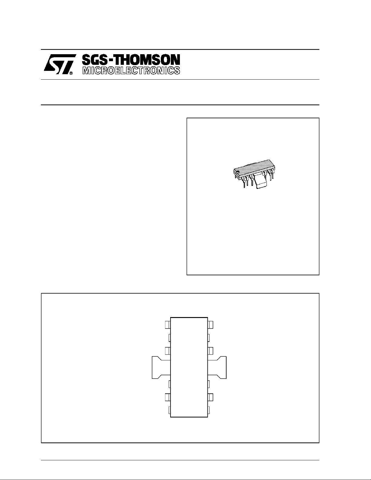
The TDA1170Sis a monolithicintegrated circuitin
a 12-lead quad in-line plastic package. It is intended for use in black and white and colour TV
receivers.
TDA1170S
TV VERTICALDEFLECTION
FINDIP
(Plastic Package)
ORDER CODE : TDA1170S
PINCONNECTIONS
POWER AMPLIFLIER OUTPUT
December 1992
RAMP OUTPUT
SUPPLY VOLTAGE
FLYBACK
GROUND
POWER AMPLIFLIER
SUPPLY VOLTAGE
REGULATED
VOLTAGE
1 12 RAMP GENERATOR
2
3
4
5
67
11
10
9
8
COMPENSATION
AMP. INPUT
GROUND
OSCILLATOR
SYNC. INPUT
HEIGHT ADJUSTMENT
1170S-01.EPS
1/9
Page 2
TDA1170S
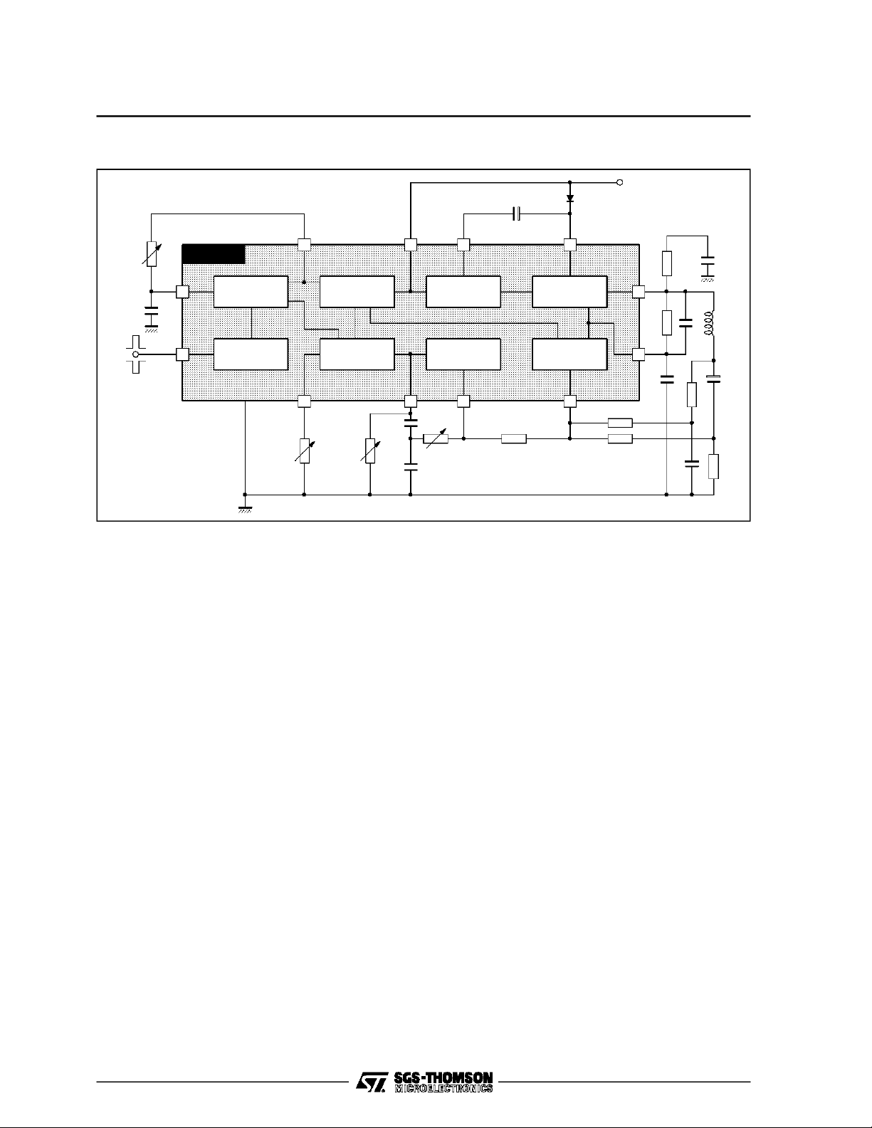
BLOCK DIAGRAM
C
4
D
A
+V
S
FREQ
SYNC
P
TDA1170S
1
OSCILLATOR
9
C
1
8
SYNC
CIRCUIT
TABS
6
VOLTAGE
REGULATOR
RAMP
GENERATOR
712110
2
HEIGHT
R
C
A
2
2
FLYBACK
GENERATOR
BUFFER
STAGE
LINEARITY
PP
3
C
3
35
AMPLIFLIER
PREAMPLIFLIER
R
B
POWER
4
R
G
11
57
R
D
R
C
C
R
9
H
YOKE
C
8
CC
R
E
C
6
R
F
1170S-02.EPS
2/9
Page 3
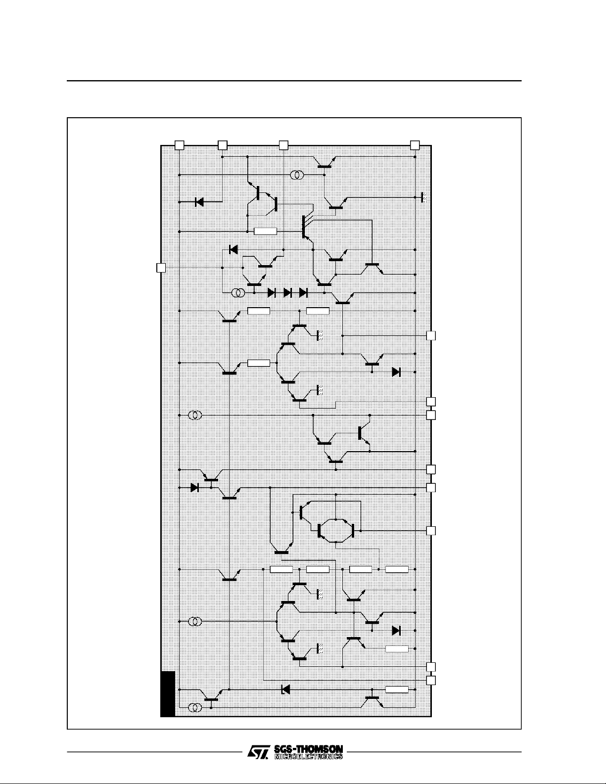
SCHEMATICDIAGRAM
TDA1170S
TABS
2
3
4
Q37
D8
5
D7
Q36
Q28
Q35
R10
Q29
D4
D5
D6
Q33
Q30
Q34
Q31
Q32
Q27
R8
Q26
R7
Q25
Q22
Q21
Q23
Q20
R9
Q24
D3
178101112
Q18
Q17
Q16
Q19
TDA1170S
Q1
Q15
Q10
Q11
R3
Z1
Q5
Q4
Q12
Q13
Q14
R5
B
A
R4
Q6
Q3
Q9
C
Q7
D
Q8
R6
E
D1
R2
69
R1
Q2
1170S-03.EPS
3/9
Page 4

TDA1170S
ABSOLUTE MAXIMUM RATINGS
Symbol Parameter Value Unit
V
S
V
4,V5
V
10
I
o
I
o
I
o
I
3
I
3
I
8
P
tot
T
stg,Tj
THERMALDATA
Symbol Parameter Value Unit
R
th j–tab
R
th j–amb
(°)Obtained with tabs soldered to printed circuitwith minimized copper area.
Supply Voltage at Pin 2 35 V
Flyback Peak Voltage 60 V
Power Amplifier Input Voltage + 10
– 0.5
Output Peak Current (non repetitive) at t = 2msec 2 A
Output Peak Current at f = 50Hz t ≤ 10µsec 2.5 A
Output Peak Current at f = 50Hz t > 10µsec 1.5 A
Pin 3 DC Current at V42 100 mA
Pin 3 Peak to Peak Flyback Current for f = 50Hz, t
≤ 1.5msec 1.8 A
fly
Pin 8 Current ± 20 mA
Power Dissipation : at T
at T
=90°C
tab
amb
=80°C
5
1
Storage and Junction Temperature – 40, + 150 °C
Thermal Resistance Junction–tab Max 12 °C/W
Thermal Resistance Junction-ambient Max 70 °C/W
V
V
W
W
1170S-01.TBL
1170S-02.TBL
ELECTRICAL CHARACTERISTICS
(refer to the test circuits, V
= 35V, T
S
=25°C,unless otherwise specified)
amb
DC CHARACTERISTICS
Symbol Parameter Test Conditions Min. Typ. Max. Unit Fig.
I
2
I
5
–I
–I
–I
–I
∆I
12
I
12
V
V
1
V
3
V
4
V
4L
V
4H
V
6
V
7
∆V
6
,
∆V
S
V
10
R8 Pin 8 Input Resistance V
Pin 2 Quiescent Current I3=0 7 14 mA 1b
Pin 5 Quiescent Current I4=0 8 15 mA 1b
Oscillator Bias Current V9= 1V 0.1 1 µA1a
9
Amplifier Input Bias Current V10= 1V 0.1 1 µA1b
10
Ramp Generator Bias Current V12= 0 0.02 0.3 µA1a
12
Ramp Generator Current I7=20µA, V12= 0 19 20 24 µA1b
12
= 0 to 12V, I7=
∆V
Ramp Generator Non-linearity
Supply Voltage Range 10 35 V –
s
12
20µA
0.2 1 % 1b
Pin 1 Saturation Voltage to Ground I1= 1 mA 1 1.4 V –
Pin 3 Saturation Voltage to Ground I3= 10mA 1.7 2.6 V 1a
Quiescent Output Voltage VS= 10V
4.1 4.4 4.75 V 1a
R1 = 10kΩ , R2 = 10kΩ
= 35V
V
S
R1 = 30kΩ, R2 = 10kΩ
Output Saturation Voltage to Ground – I4= 0.1A
= 0.8A
–I
4
Output Saturation Voltage to Supply I4= 0.1A
= 0.8A
I
4
8.3 8.8 9.45 V 1a
0.9
1.2
1.9
2.3VV
1.4
2.1
2.8
3.2VV
Regulated Voltage at Pin 6 6.1 6.5 6.9 V 1b
Regulated Voltage at Pin 7 I7=20µA 6.2 6.6 7 V 1b
∆V
7
Regulated Voltage Drift with Supply
Voltage
∆V
S
= 10 to 35V 1 mV/V 1b
∆V
S
Amplifier Input Reference Voltage 2.07 2.2 2.3 V –
≤ 0.4V 1 MΩ 1a
8
1c
1c
1d
1d
1170S-03.TBL
4/9
Page 5

Figure 1 : DC Test Circuit
TDA1170S
Figure1a
I8
1kΩ
1V 1V 8V
Figure1c
V3 I3
8
9
712
+Vs
32
TDA1170S
TABS
- I12-I9
+Vs
5
4
10
R2
Figure1b
V7
+Vs
I5
5
TABS
- I10
1V
1170S-05.EPS
I2
2
910
R1
6
V4
V6
1170S-04.EPS
- I12
TDA1170S
12
7
100kΩ
Figure1d
+Vs
2
94
TDA1170S
10
4V
TABS
5
I4
2
TDA1170S
10
V4L
1170S-06.EPS
1V
TABS
5
V4H
49
I4
1170S-07.EPS
5/9
Page 6

TDA1170S
ELECTRICAL CHARACTERISTICS
(refer to the testcircuit, V
= 25V ; f = 50Hz ; T
S
AC CHARACTERISTICS
Symbol Parameter Test Conditions Min. Typ. Max. Unit
Supply Current Iy= 1App 140 mA
I
s
Sync. Input Current (positive or negative) 500 µA
I
8
V
V
t
Flyback Voltage Iy= 1App 51 V
4
Peak to Peak Oscillator Sawtooth
9
Voltage
Flyback Time Iy= 1App 0.7 ms
fly
Free Running Frequency (P1+R1) = 300kΩ, C2 = 0.1 µF
f
o
∆f Synchronization Range I
∆f
∆V
∆f
∆T
Frequency Drift with Supply Voltage VS= 10 to 35V 0.005 Hz/V
S
Frequency Drift with Tab Temperature T
tab
Figure 2 : AC Test Circuit
=25oC, unless otherwisespecified)
amb
2.4 V
42.2
(P
) = 260kΩ, C2 = 0.1 µF
1+R1
= 0.5mA 14 Hz
8
= 40 to 120°C 0.01 Hz/°C
tab
48.5
Hz
Hz
1170S-04.TBL
6/9
1170S-08.EPS
Page 7

TDA1170S
Figure 3 : TypicalApplicationCircuit for LargeScreen B/W TV SET (RY=10Ω,LY=20mH, IY= 1APP)
V = 22V
S
D1
1N4001
C9
470µF
25V
C1
0.1µF
SYNC.
INPUT
C2
C11
4.7k
C3
100µF
0.1µF
R13
Ω
P1
Hold
0.15µF
25V
100kΩ
150kΩ
5
3
TABS
T
D
A
8
1
1
7
0
6
P2
Ω
Height
R2
180k
S
7
Ω
9
R1
100k
12
2
R3*
330k
11
10
R11
3.3Ω
4
R4
220kΩ
C12
1.5nF
R5**
47kΩ
1
P3
47k
Ω
Linearity
C4
0.1µF
C5
0.1µF
Ω
R6
39kΩ
C8
33pF
Tolerance 5%
*
Tolerance 2%
**
R9**
27kΩ
R8**
27kΩ
R7**
5.6k
Ω
C10
0.1µF
C6
22µF/16V
R14
210Ω
C7
1000µF/16V
YOKE
Ry = 10
Ω
Ly = 20mH
R10*
1Ω
1170S-09.EPS
TYPICAL PERFORMANCE
Symbol Parameter Value Unit
V
S
I
s
t
fly
P
tot
I
y
For safe working up to T
Operating Supply Voltage 22 V
Supply Current 145 mA
Flyback Time 0.7 ms
Power Dissipation 2.3 W
Maximum Scanning Current (peak to peak) 1.2 A
=60°C a heatsink of Rth=14°C/W is required.
amb
1170S-05.TBL
7/9
Page 8

TDA1170S
MOUNTINGINSTRUCTION
The junction to ambient thermal resistance of the
TDA1170S can be reduced by soldering the tabs
to asuitablecopperareaoftheprintedcircuitboard
(fig. 4) or to anexternal heatsink (fig. 5).
The diagramof fig. 6shows the maximumdissipable power P
and theR
tot
as a functionof the
th j-amb
side ”s” of two equal square copper areas having
a thicknessof 35 µ (1.4mil).
Figure 4 : Exampleof P.C BoardCopper Are
isUsed as Heatsink
Figure 6 : MaximumPowerDissipation and
Junction-AmbientThermal
Resistanceversus ”S”
Figure5 : Example with ExternalHeatsink
1170S-10.EPS
Figure7 : Maximum AllowablePower
Dissipationversus Ambient
Temperature
1170S-11.EPS
8/9
1170S-12.EPS
1170S-13.EPS
Page 9

PACKAGE MECHANICAL DATA : 12 PINS- PLASTICFINDIP
TDA1170S
G
e4
b1
E1
E2
E
Dimensions
D
AL
I
a1
b
c1
12
16
e5
c
e6
e3
K
D
e
7
M
F
Millimeters Inches
Min. Typ. Max. Min. Typ. Max.
A 3.8 4.05 0.150 0.159
a1 1.5 1.75 0.059 0.069
b 0.55 0.6 0.022 0.024
b1 0.3 0.35 0.012 0.014
c 1.32 0.052
c1 0.94 0.037
D 19.2 19.9 0.756 0.783
E 16.8 17.2 17.6 0.661 0.677 0.693
E1 4.86 5.56 0.191 0.219
E2 10.11 10.81 0.398 0.426
e 2.29 2.54 2.79 0.090 0.100 0.110
e3 17.43 17.78 18.13 0.686 0.700 0.714
e4 7.62 0.300
e5 7.27 7.62 7.97 0.286 0.300 0.314
e6 12.35 12.7 13.05 0.486 0.500 0.514
F 6.3 7.1 0.248 0.280
G 9.8 0.386
I 7.8 8.6 0.307 0.339
K 6.1 6.5 0.240 0.256
L 2.5 2.9 0.098 0.114
M 2.5 3.1 0.098
Information furnishedis believed to be accurateand reliable. However, SGS-THOMSON Microelectronicsassumes no responsibility
for the consequences of use ofsuch information nor for anyinfringement of patents or other rights of third partieswhich may result
from its use. Nolicence isgranted byimplication or otherwise underany patent or patent rights of SGS-THOMSON Microelectronics.
Specifications mentioned in this publication are subject to change without notice. This publication supersedes and replaces all
information previouslysupplied. SGS-THOMSON Microelectronics products are not authorized for use as criticalcomponents in life
support devices or systems without express written approvalof SGS-THOMSON Microelectronics.
PM-FDIP.EPS
FINDIP.TBL
1994 SGS-THOMSON Microelectronics - All RightsReserved
Purchase of I2C Components of SGS-THOMSON Microelectronics, conveys a license under the Philips
2
I
C Patent. Rights to use these components in a I2C system, is granted provided that the system conformsto
2
the I
C Standard Specifications as defined by Philips.
SGS-THOMSON Microelectronics GROUP OF COMPANIES
Australia - Brazil - China - France - Germany - Hong Kong - Italy- Japan- Korea - Malaysia - Malta - Morocco
The Netherlands - Singapore - Spain - Sweden - Switzerland - Taiwan - Thailand - UnitedKingdom -U.S.A.
9/9
 Loading...