

Page 1
DATA SH EET
Product specification
File under Integrated Circuits, IC01
December 1982
INTEGRATED CIRCUITS
TDA1074A
Dual tandem electronic
potentiometer circuit
Page 2

December 1982 2
Philips Semiconductors Product specification
Dual tandem electronic
potentiometer circuit
TDA1074A
GENERAL DESCRIPTION
The TDA1074A is a monolithic integrated circuit designed for use as volume and tone control circuit in stereo amplifiers.
This dual tandem potentiometer IC consists of two ganged pairs of electronic potentiometers with the eight inputs
connected via impedance converters, and the four outputs driving individual operational amplifiers. The setting of each
electronic potentiometer pair is controlled by an individual d.c. control voltage. The potentiometers operate by current
division between the arms of cross-coupled long-tailed pairs. The current division factor is determined by the level and
polarity of the d.c. control voltage with respect to an externally available reference level of half the supply voltage. Since
the electronic potentiometers are adjusted by a d.c. control voltage, each pair can be controlled by single linear
potentiometers which can be located in any position dictated by the equipment styling. Since the input feedback
impedances around the operational amplifier gain blocks are external, the TDA1074A can perform bass/treble and
volume/loudness control. It also can be used as a low-level fader to control the sound distribution between the front and
rear loudspeakers in car radio installations.
Features
• High impedance inputs to both ‘ends’ of each electronic potentiometer
• Ganged potentiometers track within 0,5 dB
• Electronic rejection of supply ripple
• Internally generated reference level available externally so that the control voltage can be made to swing positively
and negatively around a well-defined 0 V level
• The operational amplifiers have push-pull outputs for wide voltage swing and low current consumption
• The operational amplifier outputs are current limited to provide output short-circuit protection
• Although designed to operate from a 20 V supply (giving a maximum input and output signal level of 6 V), the
TDA1074A can work from a supply as low as 7,5 V with reduced input and output signal levels.
QUICK REFERENCE DATA
PACKAGE OUTLINE
18-lead DIL; plastic (SOT102); SOT102-1; 1996 July 18.
Supply voltage (pin 11) V
P
typ. 20 V
Supply current (pin 11) I
P
typ. 22 mA
Input signal voltage (r.m.s. value) V
i(rms)
max. 6 V
Output signal voltage (r.m.s. value) V
o(rms)
max. 6 V
Total harmonic distortion THD typ. 0,05 %
Output noise voltage (r.m.s. value) V
no(rms)
typ. 50 µV
Control range ∆α typ. 110 dB
Cross-talk attenuation (L/R) α
ct
typ. 80 dB
Ripple rejection (100 Hz) α
100
typ. 46 dB
Tracking of ganged potentiometers ∆G
v
typ. 0,5 dB
Supply voltage range V
P
7,5 to 23 V
Operating ambient temperature range T
amb
−30 to + 80 °C
Page 3
December 1982 3
Philips Semiconductors Product specification
Dual tandem electronic
potentiometer circuit
TDA1074A
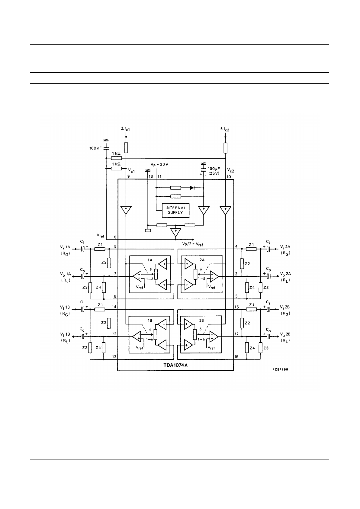
Fig.1 Block diagram and basic external components; Ic1 (at pin 9) and Ic2 (at pin 10) are control input currents;
Vc1 (at pin 9) and Vc2 (at pin 10) are control input voltages with respect to V
ref
= VP/2 at pin 8;
Z1 = Z2 = Z3 = Z4 =22 kΩ; the input generator resistance RG = 60 Ω; the output load resistance
RL = 4,7 kΩ; the coupling capacitors at the inputs and outputs are Ci = 2,2 µF and Co = 10 µF
respectively.
Page 4
December 1982 4
Philips Semiconductors Product specification
Dual tandem electronic
potentiometer circuit
TDA1074A
RATINGS
Limiting values in accordance with the Absolute Maximum System (IEC 134)
THERMAL RESISTANCE
REMARK
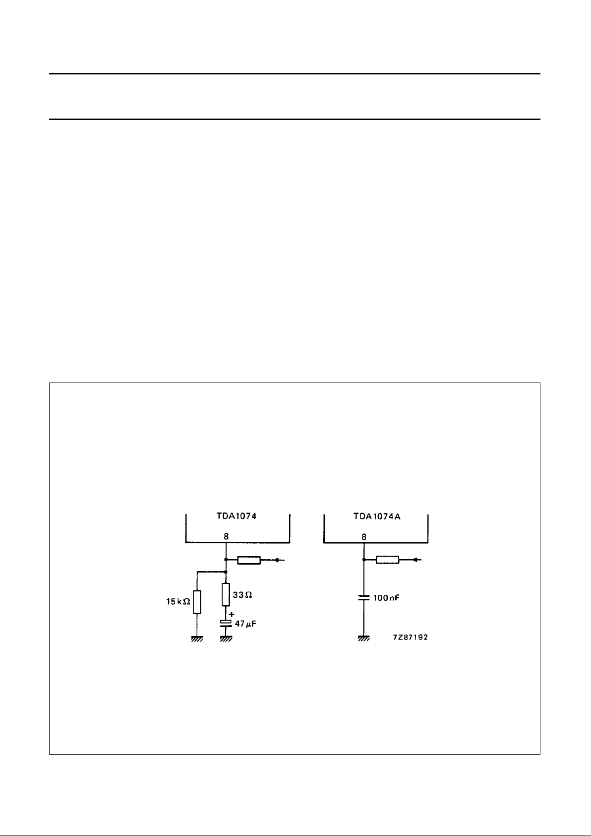
The difference between the TDA1074 and its successor the TDA1074A is shown in Fig.2 as the different component
configuration at pin 8.
Supply voltage (pin 11) V
P
max. 23 V
Control voltages (pins 9 and 10) ±V
c1
; ±V
c2
max. 1 V
Input voltage ranges (with respect to pin 18)
at pins 3, 4, 5, 6, 13, 14, 15, 16 V
i
0 to VPV
Total power dissipation P
tot
max. 800 mW
Storage temperature range T
stg
−55 to + 150 °C
Operating ambient temperature range T
amb
−30 to + 80 °C
From crystal to ambient R
th cr-a
= 80 K/W
Fig.2 Component configuration at pin 8 showing the difference between the TDA1074 and the TDA1074A.
Page 5

December 1982 5
Philips Semiconductors Product specification
Dual tandem electronic
potentiometer circuit
TDA1074A
APPLICATION INFORMATION
Treble and bass control circuit
V
P
= 20 V; T
amb
= 25 °C; measured in Fig.3; RG= 60 Ω; RL> 4,7 kΩ; CL< 30 pF; f = 1 kHz; with a linear frequency
response (V
c1
= Vc2= 0 V); unless otherwise specified
PARAMETER SYMBOL MIN. TYP. MAX. UNIT
Supply current (without load) I
P
14 22 30 mA
Frequency response (−1 dB)
V
c1
= Vc2 = 0 V f 10 − 20 000 Hz
Voltage gain at linear frequency
response (Vc1 = Vc2 = 0 V) G
v
(1)
− 0 − dB
Gain variation at f = 1 kHz
at maximum bass/treble boost or
cut at ±V
c1
= ±Vc2 = 120 mV ∆G
v
(1)
−±1−dB
Bass boost at 40 Hz (ref. 1 kHz)
Vc2 = 120 mV − 17,5 − dB
Bass cut at 40 Hz (ref. 1 kHz)
−V
c2
= 120 mV − 17,5 − dB
Treble boost at 16 kHz (ref. 1 kHz)
V
c1
= 120 mV − 16 − dB
Treble cut at 16 kHz (ref. 1 kHz)
−V
c1
= 120 mV − 16 − dB
Total harmonic distortion
at V
o(rms)
= 300 mV
f = 1 kHz (measured selectively) THD − 0,002 − %
f = 20 Hz to 20 kHz THD − 0,005 − %
at V
o(rms)
= 5 V
f = 1 kHz THD − 0,015 0,1 %
f = 20 Hz to 20 kHz THD − 0,05 0,1 %
Signal level at THD = 0,7%
(input and output) V
i; o(rms)
5,5 6,2 − V
Power bandwidth at reference
level V
o(rms)
= 5 V (−3 dB);
THD = 0,1% B − 40 − kHz
Page 6

December 1982 6
Philips Semiconductors Product specification
Dual tandem electronic
potentiometer circuit
TDA1074A
Note
1. Gv= Vo / Vi.
Output noise voltages
signal plus noise (r.m.s. value);
f = 20 Hz to 20 kHz V
no(rms)
− 75 −µV
noise (peak value); weighted to
DIN 45 405; CCITT filter V
no(m)
− 160 230 µV
Cross-talk attenuation (stereo)
f = 1 kHz α
ct
− 86 − dB
f = 20 Hz to 20 kHz α
ct
− 80 − dB
Control voltage cross-talk to
the outputs at f = 1 kHz;
V
c1(rms)
= V
c2(rms)
= 1 mV −α
ct
− 20 − dB
Ripple rejection at f = 100 Hz;
V
P(rms)
< 200 mV α
100
− 46 − dB
PARAMETER SYMBOL MIN. TYP. MAX. UNIT
Page 7

December 1982 7
Philips Semiconductors Product specification
Dual tandem electronic
potentiometer circuit
TDA1074A
Fig.3 Application diagram for treble and bass control.
Page 8

December 1982 8
Philips Semiconductors Product specification
Dual tandem electronic
potentiometer circuit
TDA1074A
Fig.4 Frequency response curves; voltage gain (treble and bass) as a function of frequency.
Fig.5 Control curve; voltage gain (bass)
as a function of the control voltage
(Vc2); f = 40 Hz.
Fig.6 Control curve; voltage gain
(treble) as a function of the
control voltage (Vc1); f = 16 kHz.
Page 9

December 1982 9
Philips Semiconductors Product specification
Dual tandem electronic
potentiometer circuit
TDA1074A
Fig.7 Voltage gain (Gv= Vo / Vi) control curves as a function of the angle of rotation (α) of a linear
potentiometer (R); for curve numbers see table above; f = 40 Hz to 16 kHz.
curve no. value of R
110kΩ
2 100 kΩ
3 220 kΩ
4 470 kΩ
51MΩ
Fig.8 Circuit diagram for measuring curves in Fig.7.
Page 10

December 1982 10
Philips Semiconductors Product specification
Dual tandem electronic
potentiometer circuit
TDA1074A
Fig.9 Output signal level as a function of VP; THD = 0,7%; f = 1 kHz; Vc1= Vc2= 0 V.
Fig.10 Total harmonic distortion as a function of the output level; VP= 20 V; RL= 4,7 kΩ; Vc1= Vc2= 0 V (linear,
G
v tot
= 1). f = 1 kHz; − − − − f = 20 kHz.
Page 11

December 1982 11
Philips Semiconductors Product specification
Dual tandem electronic
potentiometer circuit
TDA1074A
Fig.11 Power bandwidth at THD = 0,1%; reference level is 5 V (r.m.s.).
Fig.12 Cross-talk as a function of frequency; linear treble/bass setting (Vc1= Vc2= 0 V);
Vi= 5 V; RG= 60 Ω; RL= 4,7 kΩ.
Page 12

December 1982 12
Philips Semiconductors Product specification
Dual tandem electronic
potentiometer circuit
TDA1074A
Application recommendations
1. If one or more electronic potentiometers in an IC are not used, the following is recommended:
a) Unused signal inputs of an electronic potentiometer should be connected to the associated output, e.g. pins 3
and 4 to pin 2.
b) Unused control voltage inputs should be connected directly to pin 8 (V
ref
).
2. Where more than one TDA1074A IC are used in an application, pins 1 can be connected together; however, pins 8
(V
ref
) may not be connected together directly.
3. Additional circuitry for limiting the frequency response in the ultrasonic range: see Fig.13
4. Alternative circuitry for limiting the gain of the treble control circuit in the ultrasonic range: see Fig.14
(1) f
−3 dB
= 110 kHz at linear setting.
Fig.13 Circuit diagram for frequency response limiting.
Page 13

December 1982 13
Philips Semiconductors Product specification
Dual tandem electronic
potentiometer circuit
TDA1074A
For RS1= RS2= 3,3 kΩ; f
−3 dB
≅ 1 MHz at linear setting.
For RS1= RS2= 0 Ω; f
−3 dB
≅ 100 kHz at linear setting.
Fig.14 Circuit diagram for limiting gain of treble control circuit.
Page 14

December 1982 14
Philips Semiconductors Product specification
Dual tandem electronic
potentiometer circuit
TDA1074A
PACKAGE OUTLINE
REFERENCES
OUTLINE
VERSION
EUROPEAN
PROJECTION
ISSUE DATE
IEC JEDEC EIAJ
SOT102-1
93-10-14
95-01-23
UNIT
A
max.
12
b
1
(1) (1)
(1)
b
2
cD E e M
Z
H
L
mm
DIMENSIONS (inch dimensions are derived from the original mm dimensions)
A
min.
A
max.
b
max.
w
M
E
e
1
1.40
1.14
0.53
0.38
0.32
0.23
21.8
21.4
6.48
6.20
3.9
3.4
0.2542.54 7.62
8.25
7.80
9.5
8.3
0.854.7 0.51 3.7
inches
0.055
0.044
0.021
0.015
0.013
0.009
1.40
1.14
0.055
0.044
0.86
0.84
0.26
0.24
0.15
0.13
0.010.10 0.30
0.32
0.31
0.37
0.33
0.0330.19 0.020 0.15
M
H
c
(e )
1
M
E
A
L
seating plane
A
1
w M
b
1
b
2
e
D
A
2
Z
18
1
10
9
b
E
pin 1 index
0 5 10 mm
scale
Note
1. Plastic or metal protrusions of 0.25 mm maximum per side are not included.
DIP18: plastic dual in-line package; 18 leads (300 mil)
SOT102-1
Page 15

December 1982 15
Philips Semiconductors Product specification
Dual tandem electronic
potentiometer circuit
TDA1074A
SOLDERING
Introduction
There is no soldering method that is ideal for all IC
packages. Wave soldering is often preferred when
through-hole and surface mounted components are mixed
on one printed-circuit board. However, wave soldering is
not always suitable for surface mounted ICs, or for
printed-circuits with high population densities. In these
situations reflow soldering is often used.
This text gives a very brief insight to a complex technology.
A more in-depth account of soldering ICs can be found in
our
“IC Package Databook”
(order code 9398 652 90011).
Soldering by dipping or by wave
The maximum permissible temperature of the solder is
260 °C; solder at this temperature must not be in contact
with the joint for more than 5 seconds. The total contact
time of successive solder waves must not exceed
5 seconds.
The device may be mounted up to the seating plane, but
the temperature of the plastic body must not exceed the
specified maximum storage temperature (T
stg max
). If the
printed-circuit board has been pre-heated, forced cooling
may be necessary immediately after soldering to keep the
temperature within the permissible limit.
Repairing soldered joints
Apply a low voltage soldering iron (less than 24 V) to the
lead(s) of the package, below the seating plane or not
more than 2 mm above it. If the temperature of the
soldering iron bit is less than 300 °C it may remain in
contact for up to 10 seconds. If the bit temperature is
between 300 and 400 °C, contact may be up to 5 seconds.
DEFINITIONS
LIFE SUPPORT APPLICATIONS
These products are not designed for use in life support appliances, devices, or systems where malfunction of these
products can reasonably be expected to result in personal injury. Philips customers using or selling these products for
use in such applications do so at their own risk and agree to fully indemnify Philips for any damages resulting from such
improper use or sale.
Data sheet status
Objective specification This data sheet contains target or goal specifications for product development.
Preliminary specification This data sheet contains preliminary data; supplementary data may be published later.
Product specification This data sheet contains final product specifications.
Limiting values
Limiting values given are in accordance with the Absolute Maximum Rating System (IEC 134). Stress above one or
more of the limiting values may cause permanent damage to the device. These are stress ratings only and operation
of the device at these or at any other conditions above those given in the Characteristics sections of the specification
is not implied. Exposure to limiting values for extended periods may affect device reliability.
Application information
Where application information is given, it is advisory and does not form part of the specification.
 Loading...