

Page 1

DATA SH EET
Product specification
Supersedes data of August 1982
File under Integrated Circuits, IC02
May 1991
INTEGRATED CIRCUITS
TDA1023/T
Proportional-control triac triggering
circuit
Page 2
May 1991 2
Philips Semiconductors Product specification
Proportional-control triac triggering circuit TDA1023/T
FEATURES
• Adjustable width of proportional range
• Adjustable hysteresis
• Adjustable width of trigger pulse
• Adjustable repetition timing of firing burst
• Control range translation facility
• Fail safe operation
• Supplied from the mains
• Provides supply for external temperature bridge
APPLICATIONS
• Panel heaters
• Temperature control
GENERAL DESCRIPTION
The TDA1023 is a bipolar integrated circuit for controlling
triacs in a proportional time or burst firing mode. Permitting
precise temperature control of heating equipment it is
especially suited to the control of panel heaters.
It generates positive-going trigger pulses but complies with
regulations regarding mains waveform distortion and RF
interference.
QUICK REFERENCE DATA
Note
1. Negative current is defined as conventional current flow out of a device. A negative output current is suited for
positive triac triggering.
ORDERING INFORMATION
Note
1. TDA1023: 16 DIL; plastic (SOT38); SOT38-1; 1996 November 27.
2. TDA1023T: 16 mini-pack; plastic (SO16; SOT109A); SOT109-1; 1996 November 27.
SYMBOL PARAMETER MIN. TYP. MAX. UNIT
V
CC
supply voltage (derived from mains voltage) − 13.7 − V
V
Z
stabilized supply voltage for temperature bridge − 8 − V
I
16(AV)
supply current (average value) − 10 − mA
t
w
trigger pulse width − 200 −µs
T
b
firing burst repetition time at CT = 68 µF − 41 − s
-I
OH
(1)
output current −−150 mA
T
amb
operating ambient temperature range −20 − +75 °C
EXTENDED
TYPE NUMBER
PACKAGE
PINS PIN POSITION MATERIAL CODE
TDA1023 16 DIL plastic SOT38
(1)
TDA1023T 16 mini-pack plastic SO16; SOT109A
(2)
Page 3
May 1991 3
Philips Semiconductors Product specification
Proportional-control triac triggering circuit TDA1023/T
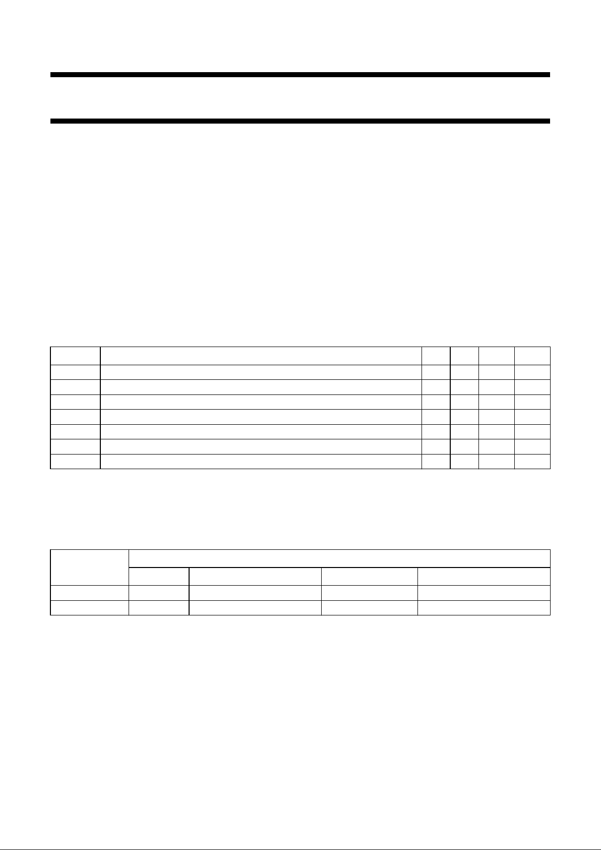
Fig.1 Block diagram.
handbook, halfpage
1
2
3
4
5
6
7
8
16
15
14
13
12
11
10
9
TDA1023
R
pd
n.c.
Q
HYS
PR
CI
UR
QR
BR
PW
TB
V
EE
V
Z
V
CC
n.c.
RX
MBA484
Fig.2 Pin configuration.
PINNING
SYMBOL PIN DESCRIPTION
R
pd
1 internal pull-down resistor
n.c. 2 not connected
Q 3 output
HYS 4 hysteresis control input
PR 5 proportional range control input
CI 6 control input
UR 7 unbuffered reference input
QR 8 output of reference buffer
BR 9 buffered reference input
PW 10 pulse width control input
V
Z
11 reference supply output
TB 12 firing burst repetition time control
input
V
EE
13 ground
V
CC
14 positive supply
n.c. 15 not connected
RX 16 external resistor connection
Page 4

May 1991 4
Philips Semiconductors Product specification
Proportional-control triac triggering circuit TDA1023/T
FUNCTIONAL DESCRIPTION
The TDA1023 generates pulses to trigger a triac. These
pulses coincide with the zero excursions of the mains
voltage, thus minimizing RF interference and mains supply
transients. In order to gate the load on and off, the trigger
pulses occur in bursts thus further reducing mains supply
pollution. The average power in the load is varied by
modifying the duration of the trigger pulse burst in
accordance with the voltage difference between the
control input CI and the reference input, either UR or BR.
Power supply: V
CC
, RX and Vz (pins 14, 16 and 11)
The TDA1023 is supplied from the AC mains via a resistor
R
D
to the RX connection (pin 16); the VEE connection (pin
13) is linked to the neutral line (see Fig.4a). A smoothing
capacitor CS should be coupled between the VCC and V
EE
connections.
A rectifier diode is included between the RX and V
CC
connections whilst the DC supply voltage is limited by a
chain of stabilizer diodes between the RX and V
EE
connections (see Fig.3).
A stabilized reference voltage (VZ) is available at pin 11 to
power an external temperature sensing bridge.
Supply operation
During the positive mains half-cycles the current through
the external voltage dropping resistor R
D
charges the
external smoothing capacitor CS until RX attains the
stabilizing potential of the internal stabilizing diodes. R
D
should be selected to be capable of supplying the current
ICC for the TDA1023, the average output current I
3(AV)
,
recharge the smoothing capacitor CS and provide the
supply for an external temperature bridge. (see Figs 9 to
12). Any excess current is by-passed by the internal
stabilizer diodes. The maximum rated supply current,
however, must not be exceeded.
During the negative mains half-cycles external smoothing
capacitor CS supplies the sum of the current demand
described above. Its capacitance must be sufficiently high
to maintain the supply voltage above the specified
minimum.
Dissipation in resistor RD is halved by connecting a diode
in series (see Fig.4b and 9 to 12). A further reduction in
dissipation is possible by using a high quality dropping
capacitor CD in series with a resistor RSD (see Figs 4c and
14). Protection of the TDA1023 and the triac against
mains-borne transients can be provided by connecting a
suitable VDR across the mains input.
Control and reference inputs CI, BR and UR
(pins 6, 9 and 7)
For the control of room temperature (5 °C to 30 °C)
optimum performance is obtained by using the translation
circuit. The buffered reference input BR (pin 9) is used as
a reference input whilst the output reference buffer QR (pin
8) is connected to the unbuffered reference input UR
(pin 7). This ensures that the range of room temperature is
encompassed in most of the rotation of the potentiometer
to give a linear temperature scale with accurate setting.
Should the translation circuit not be required, the
unbuffered reference input UR (pin 7) is used as a
reference input. The buffered reference input BR (pin 9)
must then be connected to the reference supply output V
Z
(pin 11).
For proportional power control the unbuffered reference
input UR (pin 7) must be connected to the firing burst
repetition time control input TB (pin 12).The buffered
reference input BR (pin 9), which is in this instance
inactive, must then be connected to the reference supply
output VZ (pin 11).
Proportional range control input PR (pin 5)
The output duty factor changes from 0% to 100% by a
variation of 80 mV at the control input CI (pin 6) with the
proportional range control input PR open. For temperature
control this corresponds to a temperature difference of 1 K.
By connecting the proportional range control input PR
(pin 5) to ground the range may be increased to 400 mV,
i.e. 5 K. Intermediate values may be obtained by
connecting the PR input to ground via a resistor R5
(see Table 1).
Hysteresis control input HYS (pin 4)
With the hysteresis control input HYS (pin 4) open, the
device has a built-in hysteresis of 20 mV. For temperature
control this corresponds with 0.25 K.
Hysteresis is increased to 320 mV, corresponding to 4 K,
by grounding HYS (pin 4). Intermediate values are
obtained by connecting pin 4 via resistor R4 to ground.
Table 1 provides a set of values for R4 and R5 giving a
fixed ratio between hysteresis and proportional range.
Page 5
May 1991 5
Philips Semiconductors Product specification
Proportional-control triac triggering circuit TDA1023/T
Trigger pulse width control input PW (pin 10)
The width of the trigger pulse may be adjusted to the value
required for the triac by choosing the value of the external
synchronization resistor RS between the trigger pulse
width control input PW (pin 10) and the AC mains.
The pulse width is inversely proportional to the input
current (see Fig.13).
Output Q (pin 3)
Since the circuit has an open-emitter output it is capable of
sourcing current. It is thus suited for generating
positive-going trigger pulses. The output is current-limited
and short-circuit protected. The maximum output current is
150 mA and the output pulses are stabilized at 10 V for
output currents up to that value.
To minimize the total supply current and power dissipation,
a gate resistor R
G
must be connected between the output
Q and the triac gate to limit the output current to the
minimum required by the triac (see Figs 5 to 8).
Pull-down resistor R
pd
(pin 1)
The TDA1023 includes a 1.75 kΩ pull-down resistor R
pd
between pins 1 and 13 (VEE, ground connection) intended
for use with sensitive triacs.
LIMITING VALUES
In accordance with the Absolute Maximum System (IEC 134)
SYMBOL PARAMETER MIN. MAX. UNIT
V
CC
DC supply voltage − 16 V
Supply current
I
16(AV)
average − 30 mA
I
16(RM)
repetitive peak − 100 mA
I
16(SM)
non-repetitive peak (tp < 50 µs) − 2A
V
I
input voltage, all inputs − 16 V
I
6, 7, 9, 10
input current − 10 mA
V
1
voltage on Rpd connection − 16 V
V
3, 8, 11
output voltage, Q, QR, V
Z
− 16 V
Output current
-I
OH(AV)
average − 30 mA
-I
OH(M)
peak max. 300 µs − 700 mA
P
tot
total power dissipation − 500 mW
T
stg
storage temperature range −55 +150 °C
T
amb
operating ambient temperature range −20 +75 °C
Page 6
May 1991 6
Philips Semiconductors Product specification
Proportional-control triac triggering circuit TDA1023/T
CHARACTERISTICS
VCC = 11 to 16 V; T
amb
= −20 to +75 °C unless otherwise specified
SYMBOL PARAMETER CONDITIONS MIN. TYP. MAX. UNIT
Supply
V
CC
internally stabilized supply voltage at
I16 = 10 mA
12 13.7 15 V
∆V
CC
/∆I16variation with I
16
− 30 − mV/mA
I
16
supply current at V
16-13
= 11 to 16 V;
I10 = 1mA; f = 50 Hz; pin 11 open;
V
6-13
> V
7-13
pins 4 and 5 open −−6mA
pins 4 and 5 grounded −−7.1 mA
Reference supply output V
Z
(pin 11) for external temperature bridge
V
11-13
output voltage − 8 − V
−I
11
output current −−1mA
Control and reference inputs CI, BR and UR (pins 6, 9 and 7)
V
6-13
input voltage to inhibit the output − 7.6 − V
I
6, 7, 9
input current V1 = 4 V −−2 µA
Hysteresis control input HYS (pin 4)
∆V
6
hysteresis pin 4 open 9 20 40 mV
∆V
6
hysteresis pin 4 grounded − 320 − mV
Proportional control range input PR (pin 5)
∆V
6
proportional range pin 5 open 50 80 130 mV
∆V
6
proportional range pin 5 grounded − 400 − mV
Pulse width control input PW (pin 10)
t
w
pulse width I
10(RMS)
= 1mA; f = 50 Hz 100 200 300 µs
Firing burst repetition time control input TB (pin 12)
TbC
T
firing burst repetition time, ratio to
capacitor C
T
320 600 960 ms/µF
Output of reference buffer QR (pin 8)
output voltage at input voltage:
V
8-13
V
9-13
= 1.6 V − 3.2 − V
V
8-13
V
9-13
= 4.8 V − 4.8 − V
V
8-13
V
9-13
= 8 V − 6.4 − V
Output Q (pin 3)
V
OH
output voltage HIGH −IOH = 150 mA 10 −−V
−I
OH
output current HIGH −−150 mA
Internal pull-down resistor R
pd
(pin 1)
R
pd
resistance to V
EE
1 1.75 3 kΩ
Page 7

May 1991 7
Philips Semiconductors Product specification
Proportional-control triac triggering circuit TDA1023/T
Table 1 Adjustment of proportional range and hysteresis. Combinations of resistor values giving
hysteresis >
1
⁄4proportional range.
Table 2 Timing capacitor values C
T
Note
1. Special electrolytic capacitors recommended for use with the TDA1023.
Proportional range Proportional range resistor Minimum hysteresis Maximum hysteresis resistor
R5 R4
mV kΩ mV kΩ
80 open 20 open
160 3.3 40 9.1
240 1.1 60 4.3
320 0.43 80 2.7
400 0 100 1.8
Effective DC value Marked ACspecification Catalogue number
(1)
µF µFV
68 47 25 2222 016 90129
47 33 40 - - 90131
33 22 25 - 015 90102
22 15 40 - - 90101
15 10 25 - - 90099
10 6.8 40 - - 90098
Fig.3 Internal supply connections.
handbook, halfpage
MBA483
16
RX
V
EE
V
Z
14
13
11
STABILIZER
V
CC
Page 8

May 1991 8
Philips Semiconductors Product specification
Proportional-control triac triggering circuit TDA1023/T
Fig.4 Alternative supply arrangements.
handbook, full pagewidth
MBA470
U
–
16
RX
C
S
V
EE
V
CC
14
TDA1023
AC mains
voltage
V
S
load
(heater)
R
SD
3
R
G
13
Q
handbook, full pagewidth
MBA482
U
–
16
RX
C
S
V
EE
V
CC
14
TDA1023
AC mains
voltage
V
S
load
(heater)
R
D
3
R
G
13
Q
D1
handbook, full pagewidth
MBA469
U
–
16
RX
C
S
V
EE
V
CC
14
TDA1023
AC mains
voltage
V
S
load
(heater)
BAW62
D1
BAW62
D2
R
SD
3
R
G
C
D
13
Q
a.
b.
c.
Page 9

May 1991 9
Philips Semiconductors Product specification
Proportional-control triac triggering circuit TDA1023/T
Fig.5 VS = 110 V, 50 Hz. Fig.6 VS = 220 V, 50 Hz.
Page 10

May 1991 10
Philips Semiconductors Product specification
Proportional-control triac triggering circuit TDA1023/T
Fig.7 VS = 240 V, 50Hz. Fig.8 VS = 380 V, 50 Hz.
Page 11

May 1991 11
Philips Semiconductors Product specification
Proportional-control triac triggering circuit TDA1023/T
Fig.9 VS = 110 V. Fig.10 VS = 220 V.
Page 12

May 1991 12
Philips Semiconductors Product specification
Proportional-control triac triggering circuit TDA1023/T
Fig.11 VS = 240 V. Fig.12 VS = 380 V.
Page 13

May 1991 13
Philips Semiconductors Product specification
Proportional-control triac triggering circuit TDA1023/T
Fig.13 Synchronization resistor Rs as a function of
required trigger pulse width twwith a mains
voltage Vsas a parameter.
Fig.14 Nominal value of voltage dropping capacitor
CD and power P
RSD
dissipated in a voltage
dropping resistor RSD as a function of
average supply current I
16 (AV)
with the
mains supply voltage VS as a parameter.
Page 14

May 1991 14
Philips Semiconductors Product specification
Proportional-control triac triggering circuit TDA1023/T
Fig.15 The TDA1023/T used in a 1200 to 2000 W heater with triac BT139. For component values see Table 3.
Conditions:- Mains supply; VS = 220 V; Temperature range = 5 to 30 °C.
BT139 data at Tj = 25 °C; Vgt< 1.5 V; Igt> 70 mA; IL< 60 mA
handbook, full pagewidth
MBA513
U
–
16
RX
C
S
V
CC
14
TDA1023
AC mains
voltage
V
S
load
(heater)
R
S
3
R
G
Q
D1
R
D
PW
triac
neutral
line
V
Z
CI
BR
R
pd
V
EE
QR UR HYS PR TB
C
T
11
6
9
13874512
10
1
θ
–
R
NTC
R
p
C1
R1
Page 15

May 1991 15
Philips Semiconductors Product specification
Proportional-control triac triggering circuit TDA1023/T
Table 3 Temperature controller component values (see Fig.15). Notes 1, 2
Notes
1. ON/OFF control: pin 12 connected to pin 13.
2. If translation circuit is not required: slider of R
p
to pin 7; pin 8 open; pin 9 connected to pin 11.
SYMBOL PARAMETER REMARKS VALUE
t
w
trigger pulse width see
BT139 data sheet
75 µs
R
S
synchronization resistor see Fig.13 180 kΩ
R
G
gate resistor see Fig.6 110 Ω
I
3(AV)
max. average gate current see Fig.8 4.1 mA
R4 hysteresis resistor see Table 1 n.c.
R5 proportional band resistor see Table 1 n.c.
I
16(AV)
min. required supply current 11.1 mA
R
D
mains dropping resistor see Fig.10 6.2 kΩ
P
RD
power dissipated in R
D
see Fig.10 4.6 W
C
T
timing capacitor (eff. value) see Table 2 68 µF
VDR voltage dependent resistor cat. no. 2322 593 62512 250 V AC
D1 rectifier diode BYW56
R1 resistor to pin 11 1% tolerance 18.7 kΩ
R
NTC
NTC thermistor (at 25 °C) B = 4200 K cat no. 2322 642 12223 22 kΩ
R
p
potentiometer 22 kΩ
C1 capacitor between pins 6 and 9 47 nF
C
S
smoothing capacitor 220 µF; 16 V
If R
D
and D1 are replaced by CD and R
SD
C
D
mains dropping capacitor 470 nF
R
SD
series dropping resistor 390 Ω
P
RSD
power dissipated in R
SD
see Fig.14 0.6 W
VDR voltage dependent resistor cat. no. 2322 594 62512 250 V AC
Page 16

May 1991 16
Philips Semiconductors Product specification
Proportional-control triac triggering circuit TDA1023/T
PACKAGE OUTLINES
UNIT
A
max.
1 2
b
1
cEe M
H
L
REFERENCES
OUTLINE
VERSION
EUROPEAN
PROJECTION
ISSUE DATE
IEC JEDEC EIAJ
mm
inches
DIMENSIONS (inch dimensions are derived from the original mm dimensions)
SOT38-1
92-10-02
95-01-19
A
min.
A
max.
b
max.
w
M
E
e
1
1.40
1.14
0.055
0.045
0.53
0.38
0.32
0.23
21.8
21.4
0.86
0.84
6.48
6.20
0.26
0.24
3.9
3.4
0.15
0.13
0.2542.54 7.62
0.30
8.25
7.80
0.32
0.31
9.5
8.3
0.37
0.33
2.2
0.087
4.7 0.51 3.7
0.15
0.021
0.015
0.013
0.009
0.010.100.0200.19
050G09 MO-001AE
M
H
c
(e )
1
M
E
A
L
seating plane
A
1
w M
b
1
e
D
A
2
Z
16
1
9
8
b
E
pin 1 index
0 5 10 mm
scale
Note
1. Plastic or metal protrusions of 0.25 mm maximum per side are not included.
(1) (1)
D
(1)
Z
DIP16: plastic dual in-line package; 16 leads (300 mil); long body
SOT38-1
Page 17

May 1991 17
Philips Semiconductors Product specification
Proportional-control triac triggering circuit TDA1023/T
X
w M
θ
A
A
1
A
2
b
p
D
H
E
L
p
Q
detail X
E
Z
e
c
L
v M
A
(A )
3
A
8
9
1
16
y
pin 1 index
UNIT
A
max.
A1A2A
3
b
p
cD
(1)E(1) (1)
eHELLpQZywv θ
REFERENCES
OUTLINE
VERSION
EUROPEAN
PROJECTION
ISSUE DATE
IEC JEDEC EIAJ
mm
inches
1.75
0.25
0.10
1.45
1.25
0.25
0.49
0.36
0.25
0.19
10.0
9.8
4.0
3.8
1.27
6.2
5.8
0.7
0.6
0.7
0.3
8
0
o
o
0.25 0.1
DIMENSIONS (inch dimensions are derived from the original mm dimensions)
Note
1. Plastic or metal protrusions of 0.15 mm maximum per side are not included.
1.0
0.4
SOT109-1
95-01-23
97-05-22
076E07S MS-012AC
0.069
0.010
0.004
0.057
0.049
0.01
0.019
0.014
0.0100
0.0075
0.39
0.38
0.16
0.15
0.050
1.05
0.041
0.244
0.228
0.028
0.020
0.028
0.012
0.01
0.25
0.01 0.004
0.039
0.016
0 2.5 5 mm
scale
SO16: plastic small outline package; 16 leads; body width 3.9 mm
SOT109-1
Page 18

May 1991 18
Philips Semiconductors Product specification
Proportional-control triac triggering circuit TDA1023/T
SOLDERING
Introduction
There is no soldering method that is ideal for all IC
packages. Wave soldering is often preferred when
through-hole and surface mounted components are mixed
on one printed-circuit board. However, wave soldering is
not always suitable for surface mounted ICs, or for
printed-circuits with high population densities. In these
situations reflow soldering is often used.
This text gives a very brief insight to a complex technology.
A more in-depth account of soldering ICs can be found in
our
“IC Package Databook”
(order code 9398 652 90011).
DIP
SOLDERING BY DIPPING OR BY WA VE
The maximum permissible temperature of the solder is
260 °C; solder at this temperature must not be in contact
with the joint for more than 5 seconds. The total contact
time of successive solder waves must not exceed
5 seconds.
The device may be mounted up to the seating plane, but
the temperature of the plastic body must not exceed the
specified maximum storage temperature (T
stg max
). If the
printed-circuit board has been pre-heated, forced cooling
may be necessary immediately after soldering to keep the
temperature within the permissible limit.
R
EPAIRING SOLDERED JOINTS
Apply a low voltage soldering iron (less than 24 V) to the
lead(s) of the package, below the seating plane or not
more than 2 mm above it. If the temperature of the
soldering iron bit is less than 300 °C it may remain in
contact for up to 10 seconds. If the bit temperature is
between 300 and 400 °C, contact may be up to 5 seconds.
SO
REFLOW SOLDERING
Reflow soldering techniques are suitable for all SO
packages.
Reflow soldering requires solder paste (a suspension of
fine solder particles, flux and binding agent) to be applied
to the printed-circuit board by screen printing, stencilling or
pressure-syringe dispensing before package placement.
Several techniques exist for reflowing; for example,
thermal conduction by heated belt. Dwell times vary
between 50 and 300 seconds depending on heating
method. Typical reflow temperatures range from
215 to 250 °C.
Preheating is necessary to dry the paste and evaporate
the binding agent. Preheating duration: 45 minutes at
45 °C.
W
AVE SOLDERING
Wave soldering techniques can be used for all SO
packages if the following conditions are observed:
• A double-wave (a turbulent wave with high upward
pressure followed by a smooth laminar wave) soldering
technique should be used.
• The longitudinal axis of the package footprint must be
parallel to the solder flow.
• The package footprint must incorporate solder thieves at
the downstream end.
During placement and before soldering, the package must
be fixed with a droplet of adhesive. The adhesive can be
applied by screen printing, pin transfer or syringe
dispensing. The package can be soldered after the
adhesive is cured.
Maximum permissible solder temperature is 260 °C, and
maximum duration of package immersion in solder is
10 seconds, if cooled to less than 150 °C within
6 seconds. Typical dwell time is 4 seconds at 250 °C.
A mildly-activated flux will eliminate the need for removal
of corrosive residues in most applications.
R
EPAIRING SOLDERED JOINTS
Fix the component by first soldering two diagonallyopposite end leads. Use only a low voltage soldering iron
(less than 24 V) applied to the flat part of the lead. Contact
time must be limited to 10 seconds at up to 300 °C. When
using a dedicated tool, all other leads can be soldered in
one operation within 2 to 5 seconds between
270 and 320 °C.
Page 19

May 1991 19
Philips Semiconductors Product specification
Proportional-control triac triggering circuit TDA1023/T
DEFINITIONS
LIFE SUPPORT APPLICATIONS
These products are not designed for use in life support appliances, devices, or systems where malfunction of these
products can reasonably be expected to result in personal injury. Philips customers using or selling these products for
use in such applications do so at their own risk and agree to fully indemnify Philips for any damages resulting from such
improper use or sale.
Data sheet status
Objective specification This data sheet contains target or goal specifications for product development.
Preliminary specification This data sheet contains preliminary data; supplementary data may be published later.
Product specification This data sheet contains final product specifications.
Limiting values
Limiting values given are in accordance with the Absolute Maximum Rating System (IEC 134). Stress above one or
more of the limiting values may cause permanent damage to the device. These are stress ratings only and operation
of the device at these or at any other conditions above those given in the Characteristics sections of the specification
is not implied. Exposure to limiting values for extended periods may affect device reliability.
Application information
Where application information is given, it is advisory and does not form part of the specification.
 Loading...