

Page 1
N - CHANNEL ENHANCEMENT MODE
FAST POWER MOS TRANSISTOR
TYPE V
DSS
STU10NA50 500 V < 0.6 Ω 10.2 A
R
DS(on)
I
D
STU10NA50
PRELIMINARY DATA
■ TYPICAL R
■ ± 30V GATE TO SOURCE VOLTA G E RATING
■ REPETITIVE AVA LANCHE TESTE D
■ LOW INTRINSIC CAPACITANCE
■ 100% AVALANCHE TESTED
■ GATE CHARGE MINIMIZED
■ REDUCED THRESHOLD VO LTA GE SPREA D
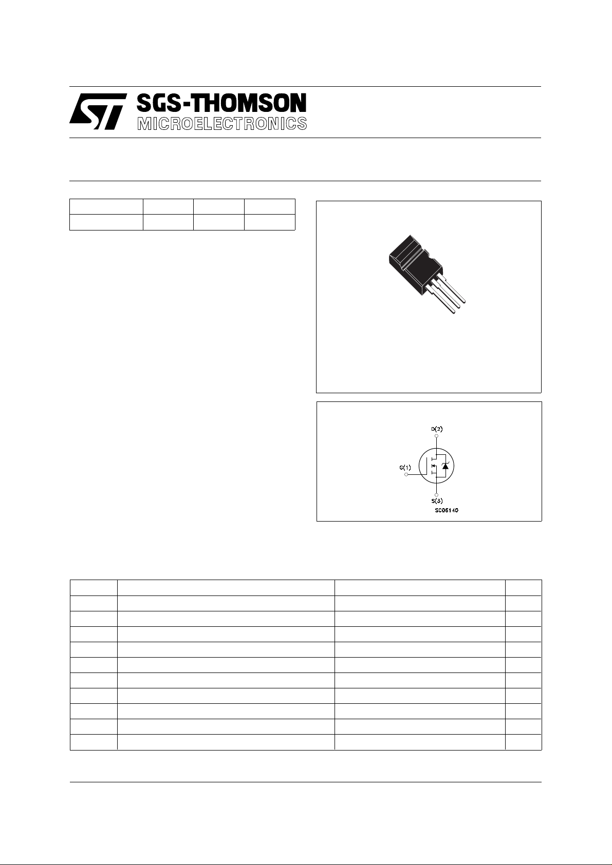
DESCRIPTION
The Max220
TM
= 0.5 Ω
DS(on)
package is a new high volume
power package exibiting the same footprint as the
industry standard TO-220, but designed to
accomodate much larger silicon chips, normally
supplied in bigger packages. The increased die
capacity makes the device ideal to reduce
component count in multiple paralleled TO-220
designs and save board space with respect to
larger packages.
APPLICATIONS
■ HIGH CURRENT, HIGH SPE ED SWI TCHING
■ SWITC H MODE POWER SUPPLIES (SMPS)
■ DC-AC CONVE RTERS FOR WELDING
EQUIPMENT AND UNINTERRUPTIBLE
POWER SU PP LIE S (UPS)
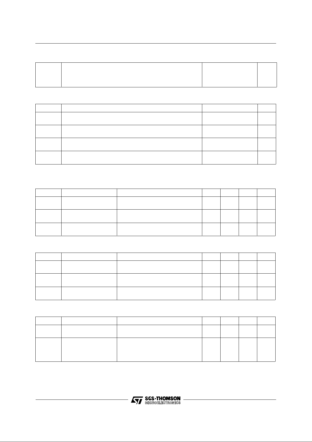
3
2
1
Max220
TM
INTER NAL SCH E M ATI C DIAG RA M
ABSOLUTE MAXIMUM RATINGS
Symbol Parameter Value Unit
V
V
V
IDM(•) Drain Current (pulsed) 40.8 A
P
T
(•) Pulse width limited by safe operating area
October 1997
DS
DGR
GS
I
D
I
D
tot
stg
T
j
Drain-source Voltage (VGS = 0) 500 V
Drain- gate Voltage (RGS = 20 kΩ)
500 V
Gate-source Voltage ± 30 V
Drain Current (continuous) at Tc = 25 oC 10.2 A
Drain Current (continuous) at Tc = 100 oC 6.4 A
Total Dissipation at Tc = 25 oC 145 W
Derating Factor 1.16 W/oC
Storage Temperature -65 to 150
Max. Operating Junction Temperature 150
o
C
o
C
1/5
Page 2
STU10NA50
THERMAL DATA
R
thj-case
Rthj-amb
R
thc-si n k
T
Thermal Resistance Junction-case Max
Thermal Resistance Junction-ambient Max
Thermal Resistance Case-sink Typ
Maximum Lead Temperature For Soldering Purpose
I
AVALANCHE CHARACTERI S TICS
Symbol Parameter Max Value Unit
I
AR
E
E
I
AR
Avalanche Current, Repetitive or Not-Repetitive
(pulse width limited by T
Single Pulse Avalanche Energy
AS
(starting T
Repetitive Avalanche Energy
AR
= 25 oC, ID = IAR, V
j
(pulse width limited by T
ma x, δ < 1%)
j
DD
ma x, δ < 1%)
j
Avalanche Current, Repetitive or Not-Repetitive
= 100 oC, pulse width limited by Tj max, δ < 1%)
(T
c
= 50 V)
0.86
30
0.1
300
10.2 A
520 mJ
24 mJ
6.8 A
o
C/W
o
C/W
o
C/W
o
C
ELECTRICAL CHARACTERISTICS (T
= 25 oC unless otherwise specified)
case
OFF
Symbol Parameter Test Conditions Min. Typ. Max. Unit
V
(BR)DSS
Drain-source
I
= 250 µA V
D
GS
= 0
500 V
Breakdown Voltage
I
DSS
I
GSS
Zero Gate Voltage
Drain Current (V
GS
Gate-body Leakage
Current (V
DS
= 0)
= 0)
= Max Rating
V
DS
V
= Max Rating x 0.8 Tc = 100 oC
DS
V
= ± 30 V
GS
250
1000µAµA
± 100 nA
ON (∗)
Symbol Parameter Test Conditions Min. Typ. Max. Unit
V
GS(th)
Gate Threshold
V
= VGS ID = 250 µA
DS
2.25 3 3.75 V
Voltage
R
DS(on)
I
D(on)
Static Drain-source On
Resistance
VGS = 10 V ID = 5 A
V
= 10 V ID = 5 A Tc = 100oC
GS
On State Drain Current VDS > I
V
= 10 V
GS
D(on)
x R
DS(on)max
0.5 0.6
1.2
10.2 A
DYNAMIC
Symbol Parameter Test Conditions Min. Typ. Max. Unit
gfs (∗) Forward
Transconductance
C
C
C
Input Capacitance
iss
Output Capacitance
oss
Reverse Transfer
rss
Capacitance
VDS > I
V
DS
x R
D(on)
DS(on)max
= 25 V f = 1 MHz V
ID = 5 A 6 9 S
= 0 1750
GS
250
80
2500
370
130
Ω
Ω
pF
pF
pF
2/5
Page 3

STU10NA50
ELECTRICAL CHARACTERISTICS (continued)
SWITCHING O N
Symbol Parameter Test Conditions Min. Typ. Max. Unit
t
d(on)
(di/dt)
Turn-on Time
Rise Time
t
r
Turn-on Current Slope V
on
V
= 250 V ID =5 A
DD
RG = 4.7 Ω VGS = 10 V
= 400 V ID = 10 A
DD
= 47 Ω VGS = 10 V
R
G
20
32
28
45
190 A/µs
ns
ns
Q
Q
Q
Total Gate Charge
g
Gate-Source Charge
gs
Gate-Drain Charge
gd
V
= 400 V ID = 10 A V
DD
= 10 V 80
GS
12
37
110 nC
SWITCHING O F F
Symbol Parameter Test Conditions Min. Typ. Max. Unit
t
r(Voff)
t
t
Off-voltage Rise Time
Fall Time
f
Cross-over Time
c
V
= 400 V ID = 10 A
DD
= 4.7 Ω VGS = 10 V
R
G
16
12
30
22
18
42
SOURCE DRAIN DIO DE
Symbol Parameter Test Conditions Min. Typ. Max. Unit
I
SD
I
SDM
V
SD
t
Q
I
RRM
(∗) Pulsed: Pulse duration = 300 µs, duty cycle 1.5 %
(•) Pulse width limited by safe operating area
Source-drain Current
(•)
Source-drain Current
10.2
40.8
(pulsed)
(∗) Forward On Voltage ISD = 10 A VGS = 0 1.6 V
Reverse Recovery
rr
Time
Reverse Recovery
rr
I
= 10 A di/dt = 100 A/µs
SD
V
= 100 V Tj = 150 oC
DD
600
10.2
Charge
Reverse Recovery
34
Current
nC
nC
ns
ns
ns
A
A
ns
µC
A
3/5
Page 4

STU10NA50
Max220 MECHANICAL DATA
DIM.
MIN. TYP. MAX. MIN. TYP. MAX.
A 4.3 4.6 0.169 0.181
A1 2.2 2.4 0.087 0.094
A2 2.9 3.1 0.114 0.122
b 0.7 0.93 0.027 0.036
b1 1.25 1.4 0.049 0.055
b2 1.2 1.38 0.047 0.054
c 0.45 0.6 0.18 0.023
D 15.9 16.3 0.626 0.641
D1 9 9.35 0.354 0.368
D2 0.8 1.2 0.031 0.047
D3 2.8 3.2 0.110 0.126
e 2.44 2.64 0.096 0.104
E 10.05 10.35 0.396 0.407
L 13.2 13.6 0.520 0.535
L1 3 3.4 0.118 0.133
mm inch
D3 D1
D2
C
A
E
A2
A1
D
b1
b2
L1
L
b
e
P011R
4/5
Page 5

STU10NA50
Information furnished is believed to be accurate and reliable. However, SGS-THOMSON Microelectronics assumes no responsability for the
consequences of use of such information nor for any infringement of patents or other rights of third parties which may results from its use. No
license is granted by implication or ot h erwise under any patent or patent rights of SGS-THOMSON Microelectronics. Specifi cations mentioned
in this publication are subject to change without notice. This publication sup ersedes and replaces all information previously supplied.
SGS-THOMSON Microelectronics products are not authorized for use as critical components in life support devices or systems without express
written approval of SGS-THOMSON Microelectonics.
© 1997 SGS-THOMSON Microelectronics - Printed in Italy - All Rights Reserved
SGS-THOMSON Microelectronics GROUP OF COMPANIES
Australia - Brazil - Canada - China - France - Germany - Hong Kong - Italy - Japan - Korea - Malaysia - Malta - Morocco - The Netherlands -
Singapore - Spain - Sweden - Switzerland - Taiwan - Thailand - United Kingdom - U.S.A
. . .
5/5
 Loading...