

Page 1
®
HIGH EFFICIENCY ULTRAFAST DIODE
MAIN PRODUCT CHARACTERISTICS
I
F(AV)
V
RRM
Tj (max) 175 °C
V
(typ) 0.78 V
F
t
(typ) 20 ns
rr
FEATURES AND BENEFITS
Suited for SMPS
■
Low losses
■
Low forward and reverse recovery times
■
Insulated package: TO-220FPAB
■
High junction temperature
■
Low leakage current
■
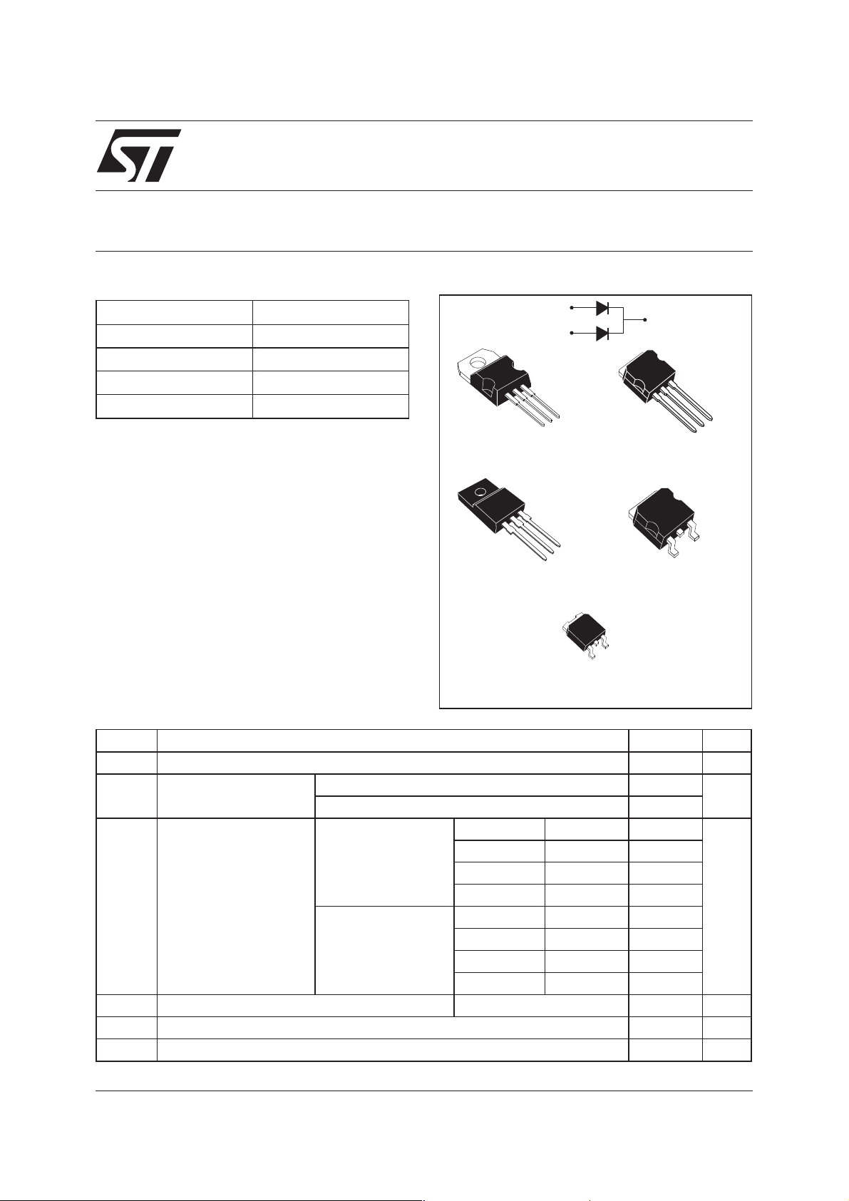
DESCRIPTION
Dual center tap rectifier suited for Switch Mode
Power Supplies and High frequency DC to DC
converters.
Packaged in DPAK, D
TO220-FPAB and I
2
PAK, this device is intended
for use in low voltage, high frequency inverters,
free wheeling and polarity protection applications.
Upto2x8A
200 V
2
PAK, TO-220AB,
TO-220AB
A1
STTH1002CT
A1
TO-220FPAB
STTH1002CFP
STTH1002CB
STTH1002C
A1
A2
A2
K
A2
K
K
K
A1
DPAK
K
I2PAK
STTH1002CR
K
D2PAK
STTH1002CG
A2
A2
K
A1
K
A2
A1
ABSOLUTE RATINGS (limiting values, per diode)
Symbol Parameter Value Unit
V
RRM
I
F(RMS)
I
F(AV)
Repetitive peak reverse voltage
RMS forward current TO-220AB / TO-220FPAB / I2PAK / D2PAK /
Average forward
current δ =0.5
I
FSM
T
stg
Tj
March 2004 - Ed: 4
Surge non repetitive forward current tp = 10 ms Sinusoidal
Storage temperature range
Maximum operating junction temperature
DPAK
TO-220AB / I2PAK
2
/D
PAK / DPAK
Tc = 155°C Per diode
Tc = 150°C Per device
Tc = 135°C Per diode
Tc = 125°C Per device
TO-220FPAB Tc = 140°C Per diode
Tc = 120°C Per device
Tc = 110°C Per diode
Tc = 75°C Per device
200 V
20 A
10
5A
10
8
16
5
10
8
16
50 A
- 65 + 175 °C
175 °C
1/8
Page 2
STTH1002C
THERMAL PARAMETERS
Symbol Parameter Maximum Unit
R
th (j-c)
Junction to case TO-220AB / I2PAK / D2PAK
/ DPAK
Per diode
Per device
TO-220FPAB Per diode
Per device
R
th (j-c)
Coupling TO-220AB / I2PAK / D2PAK / DPAK
TO-220FPAB
When the diodes 1 and 2 are used simultaneously:
∆ Tj (diode1) = P(diode1) x R
(per diode) + P(diode2) x R
th(j-c)
th(c)
STATIC ELECTRICAL CHARACTERISTICS (per diode)
Symbol Parameter Tests conditions Min. Typ. Max. Unit
4.0 °C/W
2.5
6.5
5
1.0 °C/W
3.5
*
I
R
Reverse leakage
current
**
V
F
Pulse test: * tp = 5ms, δ <2%
Forward voltage drop Tj = 25°C IF=5A
** tp = 380µs, δ <2%
Tj = 25°C V
Tj = 125°C
Tj = 25°C I
Tj = 150°C I
Tj = 150°C I
R=VRRM
=10A
F
=5A
F
=10A
F
340
0.78 0.89
5µA
1.1 V
1.25
1.05
To evaluate the maximum conduction losses use the following equation :
P = 0.73 x I
F(AV)
+ 0.032 I
F2(RMS)
DYNAMIC ELECTRICAL CHARACTERISTICS
Symbol Parameter Tests conditions Min. Typ. Max. Unit
t
rr
Reverse
recovery time
Tj = 25°C IF=1A VR= 30V
dI
/dt = 100 A/µs
F
20 25 ns
2/8
I
RM
t
fr
V
FP
Reverse
recovery current
Forward
recovery time
Forward
Tj = 125°C IF=5A VR= 160V
dI
/dt = 200 A/µs
F
Tj = 25°C IF=5A dIF/dt = 100 A/µs
V
= 1.1 x VFmax
FR
Tj = 25°C IF=5A dIF/dt = 100 A/µs
5.9 7.6 A
110 ns
2.4 V
recovery voltage
Page 3
STTH1002C
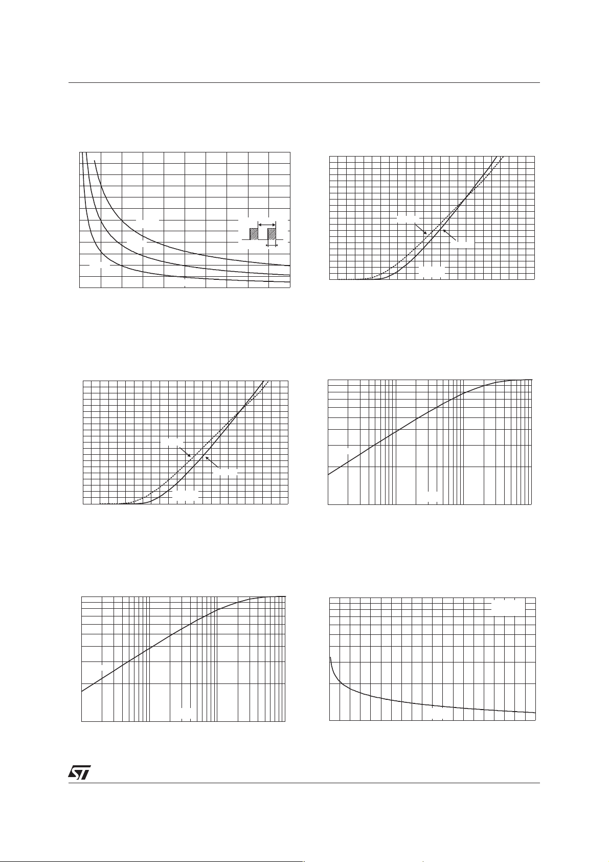
Fig. 1: Peak current versus duty cycle (per diode).
I (A)
M
60
50
40
30
20
10
P = 2W
0
0.0 0.1 0.2 0.3 0.4 0.5 0.6 0.7 0.8 0.9 1.0
P = 10W
P = 5W
δ
I
M
δ
=tp/T
T
tp
Fig. 2-2: Forward voltage drop versus forward
current (maximum values, per diode).
I (A)
FM
100
90
80
70
60
T =150°C
50
40
30
20
10
0
0.00 0.25 0.50 0.75 1.00 1.25 1.50 1.75 2.00 2.25 2.50 2.75 3.00
j
V (V)
FM
T =25°C
j
Fig. 2-1: Forward voltage drop versus forward
current (typical values, per diode).
I (A)
FM
100
90
80
70
60
50
40
30
20
10
0
0.00 0.25 0.50 0.75 1.00 1.25 1.50 1.75 2.00 2.25 2.50 2.75 3.00
T =150°C
j
V (V)
FM
T =25°C
j
Fig. 3-1: Relative variation of thermal impedance
junction to case versus pulse duration (TO-220AB,
2
PAK, D2PAK, DPAK).
I
Z/R
th(j-c) th(j-c)
1.0
Single pulse
t(s)
0.1
1.E-03 1.E-02 1.E-01 1.E+00
p
Fig. 3-2: Relative variation of thermal impedance
junction to case versus pulse duration
(TO-220FPAB).
Z/R
th(j-c) th(j-c)
1.0
Single pulse
t(s)
0.1
1.E-03 1.E-02 1.E-01 1.E+00
p
Fig. 4: Junction capacitance versus reverse
voltage applied (typical values, per diode).
C(pF)
100
V (V)
10
0 50 100 150 200
R
F=1MHz
V =30mV
OSC RMS
T =25°C
j
3/8
Page 4

STTH1002C
Fig. 5: Reverse recovery charges versus dIF/dt
(typical values, per diode).
Q (nC)
rr
240
I =5A
F
220
V =160V
R
200
180
160
140
120
100
80
60
40
20
0
10 100 1000
T =125°C
j
dI /dt(A/µs)
F
T =25°C
j
Fig. 7: Peak reverse recovery current versus dIF/dt
(typical values, per diode).
I(A)
RM
13
I =5A
F
12
V =160V
R
11
10
9
8
7
6
5
4
3
2
1
0
10 100 1000
T =125°C
j
dI /dt(A/µs)
F
T =25°C
j
Fig. 6: Reverse recovery time versus dIF/dt
(typical values, per diode).
t(ns)
rr
80
I =5A
F
V =160V
R
70
60
50
40
30
20
10
0
10 100 1000
T =125°C
j
dI /dt(A/µs)
F
T =25°C
j
Fig. 8: Dynamic parameters versus junction
temperature.
Q;rrI [T ]/Q ;I [T =125°C]
RM j rr RM j
1.4
I =5A
F
V =160V
R
1.2
1.0
I
0.8
0.6
0.4
0.2
0.0
25 50 75 100 125 150
RM
Q
rr
T (°C)
j
Fig. 9-1: Thermal resistance junction to ambient
versus copper surface under tab (Epoxy printed
circuit board FR4, e
R (°C/W)
th(j-a)
80
70
60
50
40
30
20
10
0
02468101214161820
4/8
: 35µm) for D2PAK.
CU
S(Cu)(cm²)
Fig. 9-2: Thermal resistance junction to ambient
versus copper surface under tab (Epoxy printed
circuit board FR4, e
R (°C/W)
th(j-a)
100
90
80
70
60
50
40
30
20
10
0
0 2 4 6 8 10 12 14 16 18 20
: 35µm) for DPAK.
CU
S(Cu)(cm²)
Page 5

STTH1002C
Ordering code Marking Package Weight Base qty Delivery mode
STTH1002CB STTH1002CB DPAK 0.3 g 75 Tube
STTH1002CB-TR STTH1002CB DPAK 0.3 g 2500 Tape & reel
STTH1002CT STTH1002CT TO-220AB 2.23 g 50 Tube
STTH1002CG STTH1002CG D
STTH1002CG-TR STTH1002CG D
STTH1002CR STTH1002CR I
STTH1002CFP STTH1002CFP TO-220FPAB 1.70 g 50 Tube
PACKAGE MECHANICAL DATA
DPAK
2
PAK 1.48 g 50 Tube
2
PAK 1.48g 1000 Tape & reel
2
PAK 1.49 g 50 Tube
DIMENSIONS
REF.
Millimeters Inches
Min. Max Min. Max.
A 2.20 2.40 0.086 0.094
A1 0.90 1.10 0.035 0.043
A2 0.03 0.23 0.001 0.009
B 0.64 0.90 0.025 0.035
B2 5.20 5.40 0.204 0.212
C 0.45 0.60 0.017 0.023
C2 0.48 0.60 0.018 0.023
D 6.00 6.20 0.236 0.244
E 6.40 6.60 0.251 0.259
G 4.40 4.60 0.173 0.181
H 9.35 10.10 0.368 0.397
L2 0.80 typ. 0.031 typ.
L4 0.60 1.00 0.023 0.039
V2 0° 8° 0° 8°
FOOTPRINT
6.7
6.7
3
3
1.61.6
2.32.3
5/8
Page 6

STTH1002C
PACKAGE MECHANICAL DATA
2
PAK
D
L2
E
L
L3
B2
B
G
* FLAT ZONE NO LESS THAN 2mm
C2
A1
DIMENSIONS
A
REF.
Millimeters Inches
Min. Max. Min. Max.
A 4.40 4.60 0.173 0.181
A1 2.49 2.69 0.098 0.106
D
A2 0.03 0.23 0.001 0.009
B 0.70 0.93 0.027 0.037
B2 1.14 1.70 0.045 0.067
C 0.45 0.60 0.017 0.024
C
R
C2 1.23 1.36 0.048 0.054
D 8.95 9.35 0.352 0.368
E 10.00 10.40 0.393 0.409
A2
G 4.88 5.28 0.192 0.208
L 15.00 15.85 0.590 0.624
M
*
V2
L2 1.27 1.40 0.050 0.055
L3 1.40 1.75 0.055 0.069
M 2.40 3.20 0.094 0.126
R 0.40 typ. 0.016 typ.
V2 0° 8° 0° 8°
FOOTPRINT DIMENSIONS (in millimeters)
16.90
10.30
1.30
3.70
8.90
6/8
5.08
Page 7

PACKAGE MECHANICAL DATA
2
PAK
I
E
L2
L1
b2
L
b1
b
e
c2
D
A1
STTH1002C
DIMENSIONS
REF.
A
A 4.40 4.60 0.173 0.181
A1 2.49 2.69 0.098 0.106
b 0.70 0.93 0.028 0.037
b1 1.14 1.17 0.044 0.046
b2 1.14 1.17 0.044 0.046
c 0.45 0.60 0.018 0.024
c2 1.23 1.36 0.048 0.054
D 8.95 9.35 0.352 0.368
e 2.40 2.70 0.094 0.106
E 10.0 10.4 0.394 0.409
L 13.1 13.6 0.516 0.535
L1 3.48 3.78 0.137 0.149
L2 1.27 1.40 0.050 0.055
c
Millimeters Inches
Min. Max. Min. Max.
PACKAGE MECHANICAL DATA
TO-220FPAB
H
Dia
L6
L2
L3
L5
D
L4
G1
G
F1
F2
F
DIMENSIONS
REF.
A
B
A 4.4 4.6 0.173 0.181
Millimeters Inches
Min. Max. Min. Max.
B 2.5 2.7 0.098 0.106
D 2.5 2.75 0.098 0.108
E 0.45 0.70 0.018 0.027
F 0.75 1 0.030 0.039
F1 1.15 1.70 0.045 0.067
L7
F2 1.15 1.70 0.045 0.067
G 4.95 5.20 0.195 0.205
G1 2.4 2.7 0.094 0.106
H 10 10.4 0.393 0.409
L2 16 Typ. 0.63 Typ.
L3 28.6 30.6 1.126 1.205
L4 9.8 10.6 0.386 0.417
E
L5 2.9 3.6 0.114 0.142
L6 15.9 16.4 0.626 0.646
L7 9.00 9.30 0.354 0.366
Dia. 3.00 3.20 0.118 0.126
7/8
Page 8

STTH1002C
PACKAGE MECHANICAL DATA
TO-220AB
H2
Dia
L5
L6
L2
F2
F1
F
G1
G
L9
L4
DIMENSIONS
REF.
Millimeters Inches
Min. Max. Min. Max.
A 4.40 4.60 0.173 0.181
A
C
C 1.23 1.32 0.048 0.051
D 2.40 2.72 0.094 0.107
E 0.49 0.70 0.019 0.027
L7
F 0.61 0.88 0.024 0.034
F1 1.14 1.70 0.044 0.066
F2 1.14 1.70 0.044 0.066
G 4.95 5.15 0.194 0.202
D
G1 2.40 2.70 0.094 0.106
H2 10 10.40 0.393 0.409
L2 16.4 typ. 0.645 typ.
M
E
L4 13 14 0.511 0.551
L5 2.65 2.95 0.104 0.116
L6 15.25 15.75 0.600 0.620
L7 6.20 6.60 0.244 0.259
L9 3.50 3.93 0.137 0.154
M 2.6 typ. 0.102 typ.
Diam. 3.75 3.85 0.147 0.151
■
Epoxy meets UL94,V0
■
Cooling method: by conduction (method C)
■
Recommended torque value (TO-220AB): 0.8 N.m.
■
Maximum torque value (TO-220AB): 1.0 N.m.
■
Recommended torque value (TO-220FPAB): 0.55 N.m.
■
Maximum torque value (TO-220FPAB): 0.7 N.m.
Information furnished is believed to be accurate and reliable. However, STMicroelectronics assumes no responsibility for the consequences of
use of such information nor for any infringement of patents or other rights of third parties which may result from itsuse. No license is granted by
implication or otherwise under any patent or patent rights of STMicroelectronics. Specifications mentioned in this publication are subject to
change without notice. This publication supersedes and replaces all information previously supplied. STMicroelectronics products are not au
thorized for use as critical components in life support devices or systems without express written approval of STMicroelectronics.
The ST logo is a registered trademark of STMicroelectronics.
All other names are the property of their respective owners.
© 2004 STMicroelectronics - All rights reserved.
STMicroelectronics GROUP OF COMPANIES
Australia - Belgium - Brazil - Canada - China - Czech Republic - Finland - France - Germany -
Hong Kong - India - Israel - Italy - Japan - Malaysia - Malta - Morocco - Singapore - Spain -
Sweden - Switzerland - United Kingdom - United States
www.st.com
8/8
-
 Loading...