

Page 1

STP10NB50
STP10NB50FP
N - CHANNEL 500V - 0.55Ω - 10.6A - TO-220/TO-220FP
PowerMESH MOSFET
TYPE V
STP10NB5 0
STP10NB5 0FP
■ TYPICALR
■ EXTREMELY HIGH dv/dt CAPABILITY
■ 100%AVALANCHETESTED
■ VERYLOW INTRINSICCAPACITANCES
■ GATECHARGE MINIMIZED
DS(on)
DSS
500 V
500 V
= 0.55
DESCRIPTION
Using the latesthigh voltage MESHOVERLAY
process, STMicroelectronics has designed an
advanced family of power MOSFETs with
outstanding performances. The new patent
pending strip layout coupled with the Company’s
proprietary edge termination structure, gives the
lowest RDS(on) per area, exceptional avalanche
and dv/dt capabilities and unrivalled gate charge
and switching characteristics.
R
DS(on)
<0.60Ω
<0.60
Ω
Ω
I
D
10.6 A
10.6 A
3
2
1
TO-220 TO-220FP
INTERNAL SCHEMATIC DIAGRAM
3
2
1
APPLICATIONS
■ HIGHCURRENT, HIGHSPEEDSWITCHING
■ SWITCHMODE POWER SUPPLIES(SMPS)
■ DC-AC CONVERTERS FOR WELDING
EQUIPMENTAND UNINTERRUPTIBLE
POWERSUPPLIESAND MOTOR DRIVE
ABSOLUTE MAXIMUM RATINGS
Symbol Parameter Value Unit
ST P10 NB50 ST P1 0NB50F P
V
V
V
I
DM
P
dv/ dt(
V
T
(•) Pulse width limited by safe operating area (1)ISD≤ 10.6 A, di/dt≤ 200A/µs,VDD≤ V
(*) Limited only by maximum temperatureallowed
October 1999
Drain-sour ce Voltage (VGS=0) 500 V
DS
Drain- gat e Voltage (RGS=20kΩ)
DGR
Gate-sourc e Voltage ± 30 V
GS
Drain Current ( continuous) at Tc=25oC 10.6 10.6( * ) A
I
D
Drain Current ( continuous) at Tc= 100oC6.46.4(*)A
I
D
500 V
(•) D r ain Current ( pul s ed ) 42.4 42.4 A
Total Dissipation at Tc=25oC 135 40 W
tot
Derating Fac t or 1.08 0.32 W/
1) Peak Diode Recovery voltag e slope 4.5 4.5 V/ns
Ins ulation With s t an d Voltag e (DC) 2000 V
ISO
Sto rage Te mpe r ature -65 to 150
stg
Max. Oper ating Junct ion Tem p er a t ure 150
T
j
(BR)DSS
,Tj≤T
JMAX
o
C
o
C
o
C
1/9
Page 2
STP10NB50STP10NB50FP
THERMAL DATA
TO-220 TO-220FP
R
thj-case
R
thj-amb
R
thc-sink
T
AVALANCHE CHARACTERISTICS
Symbol Para meter Max Val ue U ni t
I
AR
E
Ther mal Resis t an ce Junc ti on-cas e Max 0.93 3.12
Ther mal Resis t an ce Junc ti on-ambien t Ma x
Thermal Resistance Case-sink Typ
Maximum Lead Temper at ure For Sold er ing Purp os e
l
Avalanche Current, Repet it ive or No t -Repet it ive
(pulse width limited by T
Single Pulse Avalanche Energ y
AS
(starting T
=25oC, ID=IAR,VDD=50V)
j
max)
j
62.5
0.5
300
10.6 A
550 mJ
o
C/W
o
C/W
o
C/W
o
C
ELECTRICAL CHARACTERISTICS
=25oC unless otherwisespecified)
(T
case
OFF
Symbol Parameter Test Conditions Min. Typ. Max. Unit
V
(BR)DSS
Drain-sourc e
=250µAVGS=0
I
D
500 V
Break d own Vo lt age
I
DSS
I
GSS
Zero Gate Voltage
Drain Cu rr ent (V
GS
Gat e- b ody Leakage
Current (V
DS
=0)
=0)
V
=MaxRating
DS
= Max Rating Tc=125oC
V
DS
=± 30 V
V
GS
1
50
± 100 nA
ON(∗)
Symbol Parameter Test Conditions Min. Typ. Max. Unit
V
GS(th)
Gate Threshold
V
DS=VGSID
= 250µA
345V
Voltage
R
DS(on)
Static Drain-source On
VGS=10V ID= 5.3 A 0.55 0.60 Ω
Resistanc e
I
D(on)
On State Drain Current VDS>I
D(on)xRDS(on)max
10.6 A
VGS=10V
DYNAMIC
Symbol Parameter Test Conditions Min. Typ. Max. Unit
g
(∗)Forward
fs
Tr ansconduc tance
C
C
C
Input Capac i t ance
iss
Out put Capac it a nc e
oss
Reverse Transfer
rss
Capacitance
VDS>I
D(on)xRDS(on)maxID
=5.3 A 5 8 S
VDS=25V f=1MHz VGS= 0 1480
210
25
µ
µA
pF
pF
pF
A
2/9
Page 3
STP10NB50 STP10NB50FP
ELECTRICAL CHARACTERISTICS
(continued)
SWITCHING ON
Symbol Parameter Test Conditions Min. Typ. Max. Unit
t
d(on)
Turn-on Time
r
Rise Time
t
VDD= 250 V ID=5.3A
R
=4.7
G
Ω
VGS=10V
25
13
14
20
(see te st circuit, f igure 3)
Q
Q
Q
Total Gate Charge
g
Gat e- Source Charge
gs
Gate-Drain Charge
gd
VDD= 160 V ID=10A VGS=10V 38
10
17
49 nC
SWITCHING OFF
Symbol Parameter Test Conditions Min. Typ. Max. Unit
t
r(Voff)
t
t
Off -voltage Rise Time
Fall Time
f
Cross-ov er Ti me
c
VDD= 160 V ID=10A
=4.7 ΩVGS=10V
R
G
(see te st circuit, f igure 5)
13
15
25
11
14
28
SOURCEDRAINDIODE
Symbol Parameter Test Conditions Min. Typ. Max. Unit
I
SD
I
SDM
V
SD
t
Q
I
RRM
(∗) Pulsed: Pulse duration = 300 µs, dutycycle 1.5%
(•) Pulse width limited by safeoperating area
Source-drain Current
(•)
Source-drain Current
10.6
42.4
(pulsed)
(∗) F or ward On Voltage ISD=10.6 A VGS=0 1.6 V
Reverse Recovery
rr
Time
Reverse Recovery
rr
=10.6 A di/dt = 100 A/µs
I
SD
=50V Tj= 150oC
V
DD
(see te st circuit, f igure 5)
560
4.9
Charge
Reverse Recovery
17.5
Current
ns
ns
nC
nC
ns
ns
ns
A
A
ns
nC
A
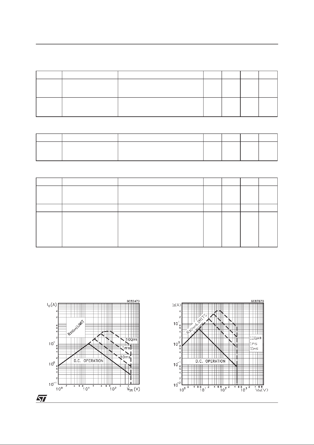
SafeOperating Area SafeOperating Area for TO-220FP
3/9
Page 4

STP10NB50STP10NB50FP
ThermalImpedencefor TO-220
OutputCharacteristics
ThermalImpedencefor TO-220FP
TransferCharacteristics
Transconductance
4/9
Static Drain-sourceOn Resistance
Page 5

STP10NB50 STP10NB50FP
Gate Charge vs Gate-sourceVoltage
Normalized GateThresholdVoltage vs
Temperature
CapacitanceVariations
Normalized On Resistance vsTemperature
Source-drainDiode ForwardCharacteristics
5/9
Page 6

STP10NB50STP10NB50FP
Fig. 1:
UnclampedInductive Load Test Circuit
Fig. 3: SwitchingTimes Test CircuitsFor
ResistiveLoad
Fig. 2:
UnclampedInductive Waveform
Fig. 4: Gate Chargetest Circuit
Fig. 5:
Test Circuit For InductiveLoad Switching
And Diode Recovery Times
6/9
Page 7

TO-220 MECHANICALDATA
STP10NB50 STP10NB50FP
DIM.
MIN. TYP. MAX. MIN. TYP. MAX.
A 4.40 4.60 0.173 0.181
C 1.23 1.32 0.048 0.051
D 2.40 2.72 0.094 0.107
D1 1.27 0.050
E 0.49 0.70 0.019 0.027
F 0.61 0.88 0.024 0.034
F1 1.14 1.70 0.044 0.067
F2 1.14 1.70 0.044 0.067
G 4.95 5.15 0.194 0.203
G1 2.4 2.7 0.094 0.106
H2 10.0 10.40 0.393 0.409
L2 16.4 0.645
L4 13.0 14.0 0.511 0.551
L5 2.65 2.95 0.104 0.116
L6 15.25 15.75 0.600 0.620
L7 6.2 6.6 0.244 0.260
L9 3.5 3.93 0.137 0.154
DIA. 3.75 3.85 0.147 0.151
mm inch
E
A
L4
D
F2
F1
G1
H2
G
F
P011C
C
D1
L2
Dia.
L5
L7
L6
L9
7/9
Page 8

STP10NB50STP10NB50FP
TO-220FPMECHANICAL DATA
DIM.
MIN. TYP. MAX. MIN. TYP. MAX.
A 4.4 4.6 0.173 0.181
B 2.5 2.7 0.098 0.106
D 2.5 2.75 0.098 0.108
E 0.45 0.7 0.017 0.027
F 0.75 1 0.030 0.039
F1 1.15 1.7 0.045 0.067
F2 1.15 1.7 0.045 0.067
G 4.95 5.2 0.195 0.204
G1 2.4 2.7 0.094 0.106
H 10 10.4 0.393 0.409
L2 16 0.630
L3 28.6 30.6 1.126 1.204
L4 9.8 10.6 0.385 0.417
L6 15.9 16.4 0.626 0.645
L7 9 9.3 0.354 0.366
Ø 3 3.2 0.118 0.126
mm inch
E
A
D
8/9
B
L3
L6
L7
¯
F1
F
G1
H
F2
123
L2
L4
G
Page 9

STP10NB50 STP10NB50FP
Information furnished is believed to be accurateand reliable.However, STMicroelectronics assumes no responsibilityfor the consequences
of use of such information nor for any infringement of patents or other rights of third parties which may result from its use. No license is
granted by implication or otherwise under any patent or patent rights of STMicroelectronics. Specificationmentioned in this publicationare
subjecttochange without notice. This publicationsupersedesandreplaces all information previouslysupplied. STMicroelectronicsproducts
are not authorized for use as critical components in life support devices or systemswithout express written approval of STMicroelectronics.
The STlogo is a trademark of STMicroelectronics
1999STMicroelectronics – Printed in Italy – All Rights Reserved
STMicroelectronics GROUP OF COMPANIES
Australia - Brazil - China - Finland - France - Germany - Hong Kong - India - Italy - Japan - Malaysia - Malta - Morocco -
Singapore - Spain - Sweden- Switzerland - United Kingdom - U.S.A.
http://www.st.com
.
9/9
 Loading...