

Page 1

STP10NB20
STP10NB20FP
N - CHANNEL ENHANCEMENT MODE
PowerMESH MOSFET
TYPE V
STP10NB20
ST P10NB20FP
■ TYPICALR
■ EXTREMELY HIGH dv/dt CAPABILITY
■ 100% AVALANCHETESTED
■ VERYLOW INTRINSIC CAPACITANCES
■ GATECHARGEMINIMIZED
DS(on)
DSS
200 V
200 V
=0.3 Ω
R
DS(on)
<0.40Ω
<0.40Ω
I
D
10 A
6A
DESCRIPTION
Using the latest high voltage MESH OVERLAY
process, SGS-Thomson has designed an
advanced family of power MOSFETs with
outstanding performances. The new patent
pending strip layout coupled with the Company’s
proprietary edge termination structure, gives the
lowest RDS(on) per area, exceptional avalanche
and dv/dt capabilities and unrivalled gate charge
and switching characteristics.
APPLICATIONS
■ HIGH CURRENT, HIGHSPEEDSWITCHING
■ SWITCHMODEPOWER SUPPLIES(SMPS)
■ DC-ACCONVERTERS FOR WELDING
EQUIPMENTAND UNINTERRUPTIBLE
POWERSUPPLIESAND MOTORDRIVE
3
2
1
TO-220 TO-220FP
INTERNAL SCHEMATIC DIAGRAM
3
2
1
ABSOLUTE MAXIMUM RATINGS
Symbol Parameter Value Unit
ST P10 NB20 ST P1 0NB20FP
V
V
DGR
V
I
DM
P
dv/dt(
V
T
(•) Pulse width limited by safe operating area (1)ISD≤ 10A, di/dt ≤ 300 A/µs,VDD≤ V
November 1997
Drain-source Voltage (VGS=0) 200 V
DS
Drain- gate Voltage (RGS=20kΩ)
Gate-s ource Voltage ± 30 V
GS
Drain Curr ent ( con ti nuous) at Tc=25oC106A
I
D
Drain Curr ent ( con ti nuous) at Tc=100oC64A
I
D
200 V
(•) Dra in Curr ent (puls e d) 40 40 A
Total Dissipation at Tc=25oC8530W
tot
Derat ing F a c t or 0.68 0.24 W/
1) Peak Diode Rec overy volt ag e slope 5.5 5. 5 V/ ns
Ins ulation Withst and Voltage ( D C) 2000 V
ISO
Storage Temperature -65 to 150
stg
Max. Operating Junct ion Tempe r ature 150
T
j
(BR)DSS
,Tj≤T
JMAX
o
C
o
C
o
C
1/9
Page 2

STP10NB20/FP
THERMAL DATA
TO-220 TO 220FP
R
thj-case
R
thj-amb
R
thc-sin k
T
AVALANCHE CHARACTERISTICS
Symbol Para met e r Max Value Uni t
I
AR
E
Ther mal Resist ance Junctio n-case M ax 1.47 4.17
Ther mal Resist ance Junctio n-ambient Max
Ther mal Resist ance Case-sink T yp
Maximum Lead Tem per a t ure For S oldering P urpose
l
Avalanche Cur rent, Repet it i v e or Not-Re petitive
(pulse width limited by T
Single Pulse Avalanche Energy
AS
(starting T
=25oC, ID=IAR,VDD=50V)
j
max, δ <1%)
j
62.5
0.5
300
10 A
150 mJ
o
C/W
o
C/W
o
C/W
o
C
ELECTRICAL CHARACTERISTICS (T
=25oC unlessotherwise specified)
case
OFF
Symbol Parameter Test Cond itions Min. Typ. Ma x. Unit
V
(BR)DSS
Drain-sourc e
=250µAVGS=0
I
D
200 V
Breakdown V oltage
I
I
DSS
GSS
Zer o Gat e V o lt age
Drain Current (V
GS
Gat e-body Leaka ge
Current (V
DS
=0)
=0)
=MaxRating
V
DS
V
=MaxRating Tc=125oC
DS
= ± 30 V
V
GS
1
10
± 100 nA
ON (∗)
Symbol Parameter Test Cond itions Min. Typ. Ma x. Unit
V
GS(th )
Gate Threshold
V
DS=VGSID
=250µA
345V
Voltage
R
DS(on)
Stati c D rain-source On
VGS=10V ID=5A 0.30 0.40 Ω
Resistance
I
D(on)
On State Drain Curre nt VDS>I
D(on)xRDS(on)max
10 A
VGS=10V
DYNAMIC
Symbol Parameter Test Cond itions Min. Typ. Ma x. Unit
g
(∗)Forward
fs
Tr ansconductanc e
C
C
C
Input Capac i t an c e
iss
Out put C apa c itance
oss
Reverse Transf er
rss
Capa cit an c e
VDS>I
D(on)xRDS(on)maxID
=5 A 3 4 S
VDS=25V f=1MHz VGS= 0 470
135
22
650
190
30
µA
µA
pF
pF
pF
2/9
Page 3
STP10NB20/FP
ELECTRICAL CHARACTERISTICS (continued)
SWITCHINGON
Symbol Parameter Test Cond itions Min. Typ. Ma x. Unit
t
d(on)
t
r
Turn-on Time
Rise Tim e
VDD=100V ID=5A
=4.7 Ω VGS=10V
R
G
10
15
(see test circuit, figure 3)
Q
Q
Q
Total Gate Charge
g
Gat e-Sour ce Cha rge
gs
Gate-Drain Charge
gd
VDD=160V ID=10A VGS=10V 17
7.5
5.5
SWITCHINGOFF
Symbol Parameter Test Cond itions Min. Typ. Ma x. Unit
t
r(Voff)
t
t
Of f - voltage Rise Time
Fall Time
f
Cross-ov er Time
c
VDD=160V ID=10A
=4.7 Ω VGS=10V
R
G
(see test circuit, figure 5)
8
10
20
SOURCE DRAIN DIODE
Symbol Parameter Test Cond itions Min. Typ. Ma x. Unit
I
SD
I
SDM
V
SD
t
Q
I
RRM
(∗) Pulsed: Pulseduration = 300 µs, duty cycle 1.5 %
(•) Pulse width limited by safe operating area
Source-drain Curre nt
(•)
Source-drain Curre nt
(pulsed)
(∗) Forward On Voltage ISD=10 A VGS=0 1.5 V
Reverse Recov er y
rr
Time
Reverse Recov er y
rr
=10 A di/dt = 100 A /µs
I
SD
=50V Tj=150oC
V
DD
(see test circuit, figure 5)
170
980
Charge
Reverse Recov er y
11.5
Current
14
20
24 nC
11
14
28
10
40
ns
ns
nC
nC
ns
ns
ns
A
A
ns
nC
A
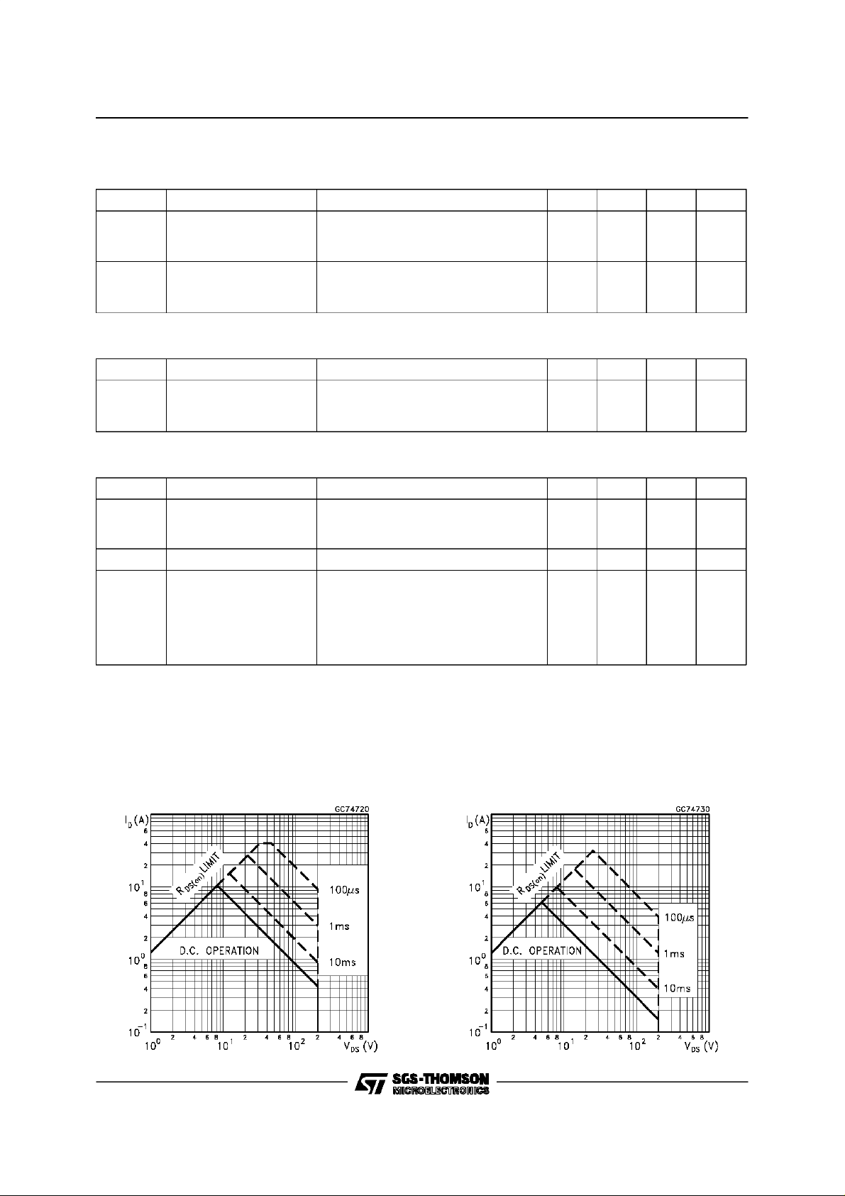
Safe Operating Area for TO-220 Safe Operating Area for TO-220FP
3/9
Page 4

STP10NB20/FP
ThermalImpedance for TO-220
OutputCharacteristics
ThermalImpedance forTO-220FP
TransferCharacteristics
Transconductance
4/9
StaticDrain-sourceOn Resistance
Page 5

STP10NB20/FP
GateCharge vs Gate-sourceVoltage
Normalized Gate Threshold Voltage vs
Temperature
CapacitanceVariations
Normalized On Resistance vs Temperature
Source-drainDiode Forward Characteristics
5/9
Page 6

STP10NB20/FP
Fig. 1: Unclamped Inductive Load TestCircuit
Fig. 3: SwitchingTimesTest CircuitsFor
ResistiveLoad
Fig. 2: Unclamped InductiveWaveform
Fig. 4: Gate Charge test Circuit
Fig. 5: Test Circuit For Inductive Load Switching
And Diode RecoveryTimes
6/9
Page 7

TO-220 MECHANICAL DATA
STP10NB20/FP
DIM.
MIN. TYP. MAX. MIN. TYP. MAX.
A 4.40 4.60 0.173 0.181
C 1.23 1.32 0.048 0.051
D 2.40 2.72 0.094 0.107
D1 1.27 0.050
E 0.49 0.70 0.019 0.027
F 0.61 0.88 0.024 0.034
F1 1.14 1.70 0.044 0.067
F2 1.14 1.70 0.044 0.067
G 4.95 5.15 0.194 0.203
G1 2.4 2.7 0.094 0.106
H2 10.0 10.40 0.393 0.409
L2 16.4 0.645
L4 13.0 14.0 0.511 0.551
L5 2.65 2.95 0.104 0.116
L6 15.25 15.75 0.600 0.620
L7 6.2 6.6 0.244 0.260
L9 3.5 3.93 0.137 0.154
DIA. 3.75 3.85 0.147 0.151
mm inch
E
A
L4
D
F2
F1
G1
F
H2
G
C
D1
L2
Dia.
L5
L7
L6
L9
P011C
7/9
Page 8

STP10NB20/FP
TO-220FP MECHANICAL DATA
DIM.
MIN. TYP. MAX. MIN. TYP. MAX.
A 4.4 4.6 0.173 0.181
B 2.5 2.7 0.098 0.106
D 2.5 2.75 0.098 0.108
E 0.45 0.7 0.017 0.027
F 0.75 1 0.030 0.039
F1 1.15 1.7 0.045 0.067
F2 1.15 1.7 0.045 0.067
G 4.95 5.2 0.195 0.204
G1 2.4 2.7 0.094 0.106
H 10 10.4 0.393 0.409
L2 16 0.630
L3 28.6 30.6 1.126 1.204
L4 9.8 10.6 0.385 0.417
L6 15.9 16.4 0.626 0.645
L7 9 9.3 0.354 0.366
Ø 3 3.2 0.118 0.126
mm inch
E
A
D
B
L3
L6
L7
¯
F1
F
G1
H
G
F2
123
L2
L4
8/9
Page 9

STP10NB20/FP
Information furnished is believed to be accurate and reliable. However,SGS-THOMSON Microelectronicsassumes no responsability for the
consequencesof use of such information nor forany infringement of patentsor other rights of third parties whichmay results from its use. No
licenseis granted by implicationor otherwise underany patent orpatent rightsof SGS-THOMSON Microelectronics. Specificationsmentioned
in this publicationare subject to change without notice. This publication supersedes andreplaces all informationpreviously supplied.
SGS-THOMSONMicroelectronics products are notauthorizedfor useas criticalcomponents in lifesupportdevices or systems withoutexpress
writtenapproval of SGS-THOMSONMicroelectonics.
1997 SGS-THOMSONMicroelectronics- Printed in Italy - All Rights Reserved
Australia- Brazil - Canada- China- France- Germany - Italy - Japan - Korea - Malaysia - Malta- Morocco - The Netherlands -
Singapore- Spain- Sweden- Switzerland- Taiwan - Thailand - United Kingdom- U.S.A
SGS-THOMSONMicroelectronics GROUP OF COMPANIES
...
9/9
 Loading...